EP1289139A2 - System and method for coupling load to communications device - Google Patents
System and method for coupling load to communications device Download PDFInfo
- Publication number
- EP1289139A2 EP1289139A2 EP02255904A EP02255904A EP1289139A2 EP 1289139 A2 EP1289139 A2 EP 1289139A2 EP 02255904 A EP02255904 A EP 02255904A EP 02255904 A EP02255904 A EP 02255904A EP 1289139 A2 EP1289139 A2 EP 1289139A2
- Authority
- EP
- European Patent Office
- Prior art keywords
- impedance
- port
- signal
- impedance matching
- load
- Prior art date
- Legal status (The legal status is an assumption and is not a legal conclusion. Google has not performed a legal analysis and makes no representation as to the accuracy of the status listed.)
- Granted
Links
Images





Classifications
-
- H—ELECTRICITY
- H03—ELECTRONIC CIRCUITRY
- H03H—IMPEDANCE NETWORKS, e.g. RESONANT CIRCUITS; RESONATORS
- H03H7/00—Multiple-port networks comprising only passive electrical elements as network components
- H03H7/38—Impedance-matching networks
- H03H7/40—Automatic matching of load impedance to source impedance
Definitions
- the present invention relates to communications. More particularly, the present invention relates to a system and method for active impedance matching in communications systems.
- the impedance of a load e.g., an antenna or a cable
- the impedance of a load is typically connected to the device using an impedance matching circuit.
- a particular problem encountered in wireless communications systems is that the impedance of an antenna typically changes with time due to the changing presence of obstacles (e.g., humans) in the vicinity of the antenna.
- obstacles e.g., humans
- the human body acts predominantly as a reflector with varying degrees of efficiency.
- the presence of one or more human bodies nearby an antenna will produce an increase in the capacitive nature of the antenna impedance, and thereby generate an impedance mismatch at the point of connection between the antenna and a wireless communications device.
- a human body proximate to an antenna affects the impedance of the antenna.
- a human body close to an antenna presents a low impedance to an RF wave.
- the presence of a human body reduces the electric field of an RF wave close by, and it increases the magnetic field.
- a high impedance is presented to an approaching RF wave front, which enhances the electric field while reducing the magnetic field. This effect is periodic, and it repeats each quarter of a wavelength of the RF wave.
- there is a deep null in a transmitted RF wave caused by the absorption of the wave by the human body. Absorption affects both the electric field and the magnetic field of an RF wave.
- the Q of an antenna should be designed so that it satisfies EQ. 1: Q ⁇ (C/ ⁇ C) where C is the tuning capacitance, and ⁇ C is the change of capacitance induced into the antenna, for example, by the proximity of a human body.
- C the tuning capacitance
- ⁇ C the change of capacitance induced into the antenna, for example, by the proximity of a human body.
- a typical value for C is 16pF
- a typical value for ⁇ C is 0.2pF (i.e., Q must be less than 80).
- the typical resistance of a small loop antenna is very low (e.g., less than 2 ⁇ ), and thus an impedance matching circuit is required even for free space radiation.
- the present invention is directed to a system and method for active impedance matching in communications systems.
- a signal sensing module senses an RF signal and produces one or more secondary signals representative of the RF signal.
- An impedance matching control module generates a control signal, based on the one or more secondary signals, which is indicative of an impedance mismatch between a load and a communications device.
- the control signal is then applied to at least one variable impedance device to adjust the impedance of an impedance matching network and thereby reduce the impedance mismatch between the load and the communications device.
- a barium strontium titanate, thin film, parallel plate capacitor is used as a variable impedance device to adjust the impedance of the impedance matching network.
- other variable impedance devices such as other types of thin film capacitors or varactor diodes can be used to adjust the impedance of the impedance matching network.
- a feature of the present invention enhances the bandwidth and/or signal-to-noise ratio of a communications system.
- Another feature of the invention enhances the operating range and battery life of portable wireless communications devices.
- the present invention provides a method and system for active impedance matching in communications systems. As described herein, the present invention is particularly well adapted for use with wireless communications devices. As will become apparent to a person skilled in the relevant communications art given the detailed description of the invention herein, it is a feature of the present invention that there is no need to reduce the Q of an antenna so that a higher gain can be achieved when using an impedance matching network according to the invention. The invention, however, is not limited to being used with wireless communications devices.
- FIG. 1 illustrates a communications system 100 according to an embodiment of the present invention.
- System 100 comprises a communications device 110, a signal sensing module 120, an impedance matching module 130, an impedance matching control module 140, and a load 150, which are coupled together as shown in FIG. 1.
- the logic and the active control devices of system 100 as well as the logic and the active control devices other system embodiments of the invention, can be implemented using standard CMOS technology.
- Communication device 110 comprises a receiver, a transmitter, and/or a transceiver, or any combination thereof.
- the function of communications device 110 is to generate an RF information signal from a baseband information signal and/or to generate a baseband information signal from an RF information signal, in a manner that would be known to one skilled in the relevant communications art.
- Communications device 110 can comprise any device that up-converts and/or down-converts electromagnetic signals of the type used for RF communications.
- Signal sensing module 120 is used to sense a transmitted and/or received RF signal.
- Signal sensing module 120 has at least three ports 122, 124, and 126 for coupling to other devices of communications system 100.
- port 122 of signal sensing module 120 is coupled to communications device 110.
- Port 124 is coupled to impedance matching module 140.
- Port 126 is coupled to impedance matching module 130.
- signal sensing module 120 can have more than three port (See, e.g., FIG. 3).
- Signal 202 in FIG. 2 illustrates an example voltage standing wave produced by an impedance mismatch between load 150 and communications device 110.
- signal sensing module 120 generates two voltage signals. One voltage signal is proportional to the incident voltage (V i ) at load 150, and a second voltage signal is proportional to the reflected voltage (V r ). These values are illustrated in FIG. 2.
- signal sensing module 120 may generate a single signal proportional to the voltage standing wave ratio (VSWR) of signal 202 or a single signal proportional to a current standing wave ratio (ISWR) of a sensed signal (not shown). The value of either a VSWR or a ISWR is indicative of the impedance mismatch between load 150 and communications device 110.
- VSWR voltage standing wave ratio
- ISWR current standing wave ratio
- Other possibilities for generating one or more signals to represent the sensed RF signal also exist, as would be known to a person skilled in the relative communications art.
- Impedance matching module 130 is used to match an impedance of load 150 to an impedance of communications device 110.
- impedance matching module 130 comprises one or more devices whose impedance can be varied in order to reduce an impedance mismatch between the impedance of load 150 and the impedance of communications device 110.
- impedance matching module 130 comprises one or more thin film capacitors.
- impedance matching module 130 comprises one or more other electronic devices whose impedance can be varied using a control signal (e.g., a bias voltage).
- Impedance matching module 130 has at least three ports 132, 134, and 136. Port 132 is coupled to signal sensing module 120. Port 134 is coupled to impedance matching control module 140. Port 136 is coupled to load 150.
- Impedance matching control module 140 generates at least one control signal that is used to varying the impedance of impedance matching module 130.
- impedance matching control module 140 generates one or more DC bias signal that are provided to impedance matching module 130 to control the impedance of impedance matching module 130.
- Impedance matching module 140 has at least two ports 142 and 144. Port 142 is coupled to signal sensing module 120. Port 144 is coupled to impedance matching module 130. As will be apparent to a person skilled in the relevant communication art from the description of the invention herein, the exact implementation of impedance matching control module 140 is dependent upon the output of signal sensing module 120 and the type and magnitude of the signal needed to control the impedance of impedance matching module 130.
- impedance matching control module 140 comprises logic, which may include, for example, memory and a lookup table, to generate a DC bias signal proportional to a VSWR of a sensed RF signal (given input signals from signal sensing module 120 that are proportional to V i and V r of the sensed RF signal).
- impedance matching control module 140 comprises circuitry to amplify the generated DC bias signal to a voltage range that can be used to control impedance matching module 130. For example, in embodiments of the invention, a DC bias voltage in the range of about 0 volts to about 9 volts can be used to control certain thin film parallel plate capacitors according to the invention and thereby change the impedance of impedance matching module 130. How to implement impedance matching control module 140 for a given signal sensing module 120 and a given impedance matching module 130 will be apparent to a person skilled in the relevant communications and/or electronics art.
- Load 150 is a load of a type typically coupled to a communications device.
- load 150 can be an antenna or a cable.
- a characteristic of load 150 is that its impedance may change with time.
- FIG. 3. illustrates a second example system 300 according to an embodiment of the present invention.
- System 300 comprises a transmitter 310, a signal sensing module 320, an impedance matching module 330, an impedance matching control module 340, and an antenna 350, which are coupled together as shown in FIG. 3.
- Each of the devices that comprise system 300 operate in a manner similar to that described above for system 100, or in a manner that would be known to a person skilled in the relevant communications art given the description of the invention herein.
- signal sensing module 320 comprises two directional couplers 322 and 324 and a delay 326.
- Each of the directional couples 322 and 324 operate in a manner that would be known to a person skilled in the relevant communications art. For example, a signal input a port 361 of directional coupler 322 is reproduced at port 365, and a signal proportional to the signal input at port 361 is produced at port 363. If a signal is input at port 365 of directional coupler 322, the signal input at port 365 will be reproduced at port 361, but no signal proportional to the signal input at port 365 is produced at port 363.
- a four-port directional coupler is used, which produces a signal proportional to the signal input at port 365 at a fourth port (not shown).
- Directional couplers 322 and 324 are coupled to delay 326.
- delay 326 is a line that is ⁇ /4 long, where ⁇ is the length of a period of a carrier signal being transmitted by transmitter 310.
- the purpose of delay 326 is to separate directional couplers 322 and 324 by the distance ⁇ /4 so that they can be used to determine both an incident wave and a reflected wave caused by an impedance mismatch between the impedance of antenna 350 and the impedance of transmitter 310.
- directional coupler 322 generates a secondary signal that can be used to determine the voltage of the wave incident at antenna 350
- directional coupler 324 generates a secondary signal that can be used to determine the voltage of the wave reflected at antenna 350.
- the secondary signals developed by signal sensing module 320 are used by impedance matching control module 340 to generate at least one DC bias voltage that is proportional to the instantaneous impedance mismatch between antenna 350 and transmitter 310.
- the bias signal or signals generated by impedance matching control module 340 are then applied to one or more variable impedance device (not shown) to adjust the impedance of impedance matching module 330.
- the impedance of impedance matching module 330 By adjusting the impedance of impedance matching module 330, the instantaneous impedance mismatch between antenna 350 and transmitter 310 is reduced.
- FIG. 4 illustrates an impedance matching module (network) 430 according to an embodiment of the invention coupled to an antenna 450.
- Impedance matching module 430 is an L-shaped network that comprises two variable capacitors 402 and 404.
- Antenna 450 is represented in FIG. 4 as an inductor 406 and a resistance 408.
- capacitors 402 and 404 are barium strontium titanate, thin film, parallel plate capacitors. Capacitor 404 is used to reduce the inductive nature of the antenna 450. Capacitor 402 is used to adjust the resonance frequency of the network. By adjusting the values of capacitors 402 and 404, impedance matching module 430 can be instantaneous tuned to match the impedance of antenna 450 to an impedance of a communications device (not shown).
- the instantaneous values of capacitors 402 and 404 are controlled using a feedback loop that comprises a signal sensing module and an impedance matching control module.
- impedance matching module 430 is automatically reconfigured to compensate for the change in the impedance of antenna 450 and reduce any resulting impedance mismatch between the impedance of antenna 450 and the impedance of a communications device.
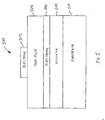
- FIG. 5 illustrates a thin film capacitor 500 according to an embodiment of the invention.
- Capacitor 500 can be formed to have a thickness ranging from about 500 ⁇ m to about 1500 ⁇ m.
- Capacitor 500 can be formed on a silicon wafer.
- Capacitor 500 comprises five layers 502, 504, 506, 508, and 510 of material.
- Capacitor 500 is formed from a ferroelectric material.
- a ferroelectric material is a nonlinear dielectric having a permittivity that is a function of an applied electric field.
- the capacitance of capacitor 500 is given by EQ. 2.
- C ⁇ .
- a d where: C is the capacitance of the capacitor, ⁇ is permittivity of the dielectric (ferroelectric) material; A is area of an electrode, and d is separation distance of the electrodes.
- EQ. 2 as the permittivity of capacitor 500 varies, so does its capacitance.
- capacitor 500 is formed to have the following characteristics.
- Layer 510 is a substrate such as, for example, silicon (e.g., a silicon wafer). In one embodiment, layer 510 has a thickness of about 500 microns.
- Layer 508 is silicon dioxide (SiO 2 ) having a thickness of about 600-800 ⁇ .
- Layer 506 is a layer of about 1500 ⁇ of platinum. Layer 506 acts as a bottom contact for capacitor 500, and it is typically used as a ground contact. Layer 506 can be deposited onto layer 508 using known deposition techniques.
- Layer 504 is a thin film having a thickness on the order of about 3000-6000 ⁇ . Layer 504 can be grown using metalorganic chemical vapor deposition (MOCVD).
- MOCVD metalorganic chemical vapor deposition
- layer 504 comprises barium strontium titanate (Ba 0.7 Sr 0.3 TiO 3 ).
- MOCVD is a preferred means growing a barium strontium titanate thin film because it provides good composition control, homogeneity of the film, and large area coverage.
- Layer 502 is a layer of about 1500 ⁇ of platinum. After deposition of layer 504, layer 502 can be deposited using a known sputtering method. To obtain the best electrical properties, layer 502 (i.e., the top electrode) must be anneal after deposition at about 520°C for about 25 minutes in air. By using this annealing process, dielectric dispersion and loss in the thin film of layer 504 film are reduced.
- FIG. 6 illustrates a typical x-ray diffraction pattern for a barium strontium titanate (BST) thin film capacitor 500, formed on silicon, and using platinum electrodes.
- the pattern shows perovskite single phase.
- the presence of only BST 100, BST 110 and BST 200 reflections indicates that only crystalline orientations are present.
- a comparison with high purity powder diffraction data indicates that a predominant orientation is x00 normal to the substrate plane. This orientation is important because it guarantees a uniform microstructure and desirable electrical properties.
- An important factor in accordance with the invention in reducing the loss in the thin film of layer 504 is the presence of titanium in excess in a range between about 1-3 %. This titanium excess also reduces the permittivity of the thin film material.
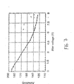
- FIG. 7 A typical permittivity of a 650 ⁇ barium strontium titanate thin film capacitor 500, operating at 1 GHz, for different bias voltage is illustrated in FIG. 7. As can be seen in FIG. 7, a change of 28% in the permittivity is observed at I GHz with a bias voltage of 6 volts. The corresponding loss tangent values are in the range of 0.04.
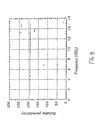
- FIG. 8 The behavior of a barium strontium titanate capacitor 500 versus frequency is illustrated in FIG. 8. As can be seen, a very low dielectric dispersion (e.g., less then 1%) is obtainable, making a barium strontium titanate capacitor 500 according to the invention an ideal variable impedance device for broadband applications according to the invention.
- thin film capacitors 500 according to the invention are to be formed directly on a silicon substrate, for example, utilizing the back side of a chip. This choice guarantees minimal wafer contamination, and it permits large areas to be used for forming the capacitors 500.
- variable impedance devices other than thin film capacitors are used.
- impedance matching module 130 comprises one or more varactor diodes.
- a varactor diode is a semiconductor device whose capacitance is a function of an applied reverse voltage, as would be known to a person skilled in the relevant arts.
- Other types of controllable impedance devices can also be used form an active impedance matching network in accordance with the invention.
- FIGs. 6-7 are illustrative and not intended to limit the invention.
- Other variable impedance devices according to the invention can have other characteristics.
- FIG. 9 illustrates one possible implementation of a system according to the invention on a integrated circuit (IC) chip900.
- IC chip 900 comprises a silicon substrate 510, a silicon oxide insulator 508, a ground plane 506, a barium strontium titanate (BST) thin film 504, and capacitor top contacts 502.
- BST barium strontium titanate
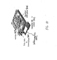
- FIG. 10 A means for interconnection of the capacitors top electrode 502 to the IC chip 900 is illustrated in FIG. 10. As shown in FIG. 10, an interconnection 1002 can be formed using a via hole 1004 through the silicon substrate 510 and through a hole 1006 in the ground plane 506.
- FIG. 11 illustrates a flowchart of a method 1100 for matching an impedance of a load to an impedance of a communications device.
- This method can be implemented using system embodiments of the present invention (e.g., system 100), and it is described with reference to the features illustrated in FIG. 1. As described below, the method comprises three steps 1110, 1120, and 1130.
- a signal sensing module 120 is used to sense a radio frequency signal.
- the radio frequency signal sensed is representative of an impedance mismatch between the impedance of load 150 and communications device 110.
- signal sensing module 120 is used to obtain a first signal that is representative of a voltage wave incident at load 150, and to obtain a second signal that is representative of a voltage wave reflected at load 150.
- the output or outputs of signal sensing module 120 are provided to impedance matching control module 140.
- impedance matching control module 140 is used to generate a control signal, using the signal or signals obtained from signal sensing module 120, that is indicative of an impedance mismatch between load 150 and communications device 110.
- the generated control signal is one or more DC bias signals, in a range between 0 and 10 volts.
- Other control signals are generated in other embodiments of the invention.
- step 1130 the control signal generated in step 1120 is applied to a variable impedance device to adjust an impedance of an impedance matching network 130. Adjusting the impedance of impedance matching network 130 reduces the impedance mismatch between the load 150 and the communications device 110,
- the variable impedance device of impedance matching network 130 is a thin film parallel plate capacitor 500.
Landscapes
- Transceivers (AREA)
- Transmitters (AREA)
- Mobile Radio Communication Systems (AREA)
Abstract
Description
As can be seen by EQ. 2, as the permittivity of
Claims (26)
- A system for coupling a load to a communications device, comprising:wherein said first port of said signal sensing module is for coupling to the communications device, said second port of said signal sensing module is coupled to said first port of said impedance matching module, said third port of said signal sensing module is coupled to said first port of said impedance matching control module, said second port of said impedance matching control module is coupled to said third port of said impedance matching module, and said second port of said impedance matching module is for coupling to the load.a signal sensing module having at least a first, second, and third port;an impedance matching module having at least a first, second, and third port; andan impedance matching control module having at least a first and second port,
- The system of claim 1, wherein said signal sensing module comprises a first directional coupler having at least a first and second port, said first port for coupling to the communications device, and said second port coupled to said impedance matching control logic module.
- The system of claim 2, wherein said signal sensing module further comprises a second directional coupler having at least a first, second, and third port; and
a delay having a first and second port,
wherein said first port of said delay is coupled to a third port of said first directional coupler, said second port of said delay is coupled to said first port of said second directional coupler, said second port of said direction coupler is coupled to said impedance matching control module, and said third port of said second directional coupler is for coupling to the load. - The system of any of claims 1 to 3, wherein said impedance matching module comprises:a first thin film capacitor, a permittivity of said first thin film capacitor being a function of a bias voltage applied to said first thin film capacitor.
- The system of claim 4, wherein said first thin film capacitor is a barium strontium titanate capacitor.
- The system of claim 4 or claim 5, wherein said capacitor is a parallel plate capacitor fabricated on a semiconductor wafer.
- The system of any of claims 4 to 6, wherein said capacitor has a thickness in a range from about 500 microns to about 1,500 microns.
- The system of any of claims 4 to 7, wherein said impedance matching module further comprises:a second thin film capacitor, a permittivity of said second thin film capacitor being a function of a bias voltage applied to said second thin film capacitor.
- The system of claim 8, wherein said first and second capacitors are parallel plate capacitors fabricated on a semiconductor wafer.
- The system of claim 9, wherein said first and second thin film capacitors ate barium strontium titanate capacitors.
- A method for matching an impedance of a load to an impedance of a communications device, comprising the steps of:(1) sensing a radio frequency signal;(2) generating a control signal, based on the radio frequency 5 signal, that is indicative of an impedance mismatch between the load and the communications device; and(3) applying the control signal to a variable impedance device to adjust an impedance of the thin film capacitor thereby reducing the impedance mismatch between the load and the communications device.
- The method of claim 11, wherein step (1) comprises the steps of:obtaining a first signal that is representative of a voltage wave incident at the load; andobtaining a second signal that is representative of a voltage wave reflected at the load.
- The method of claim 12, wherein the first and second signals are obtained using a first and second directional coupler.
- The method of any of claims 11 to 13, wherein the control signal is a DC voltage.
- The method of any of claims 11 to 14, wherein the variable impedance device is a thin film parallel plate capacitor.
- The method of claim 15, wherein the variable impedance device is a barium strontium titanate capacitor.
- The method of any of claims 11 to 14, wherein the variable impedance device is a varactor diode.
- A method according to any of claims 11 to 17, wherein the load is an antenna.
- A system for coupling a load to a communications device, comprising:an impedance matching module that couples the communications device to the load, said impedance matching module comprising a variable impedance device having a controllable impedance;a signal sensing module, coupled to the communications device and the load, that develops a reference signal proportional to a signal being transferred between the communications device and the load; andan impedance matching control module, coupled to said impedance matching module and said signal sensing module, that generates a control signal, based on said reference signal, for controlling the impedance of said variable impedance device.
- The system of claim 19, wherein said variable impedance device is a parallel plate capacitor having a ferroelectric thin film dielectric.
- The system of claim 20, wherein said ferroelectric thin film dielectric is barium strontium titanate.
- The system of claim 20 or claim 21, wherein said capacitor is fabricated on a semiconductor wafer.
- The system of any of claims 19 to 22, wherein said capacitor has a thickness in a range from about 500 microns to about 1,500 microns.
- The system of any of claims 19 to 23, wherein said impedance matching module further comprises:a second thin film capacitor.
- The system of any of claims 19 to 24, wherein said variable impedance device is a capacitor having a permittivity that is a function of an applied bias voltage.
- The system of any of claims 19 to 25, wherein the load is an antenna.
Applications Claiming Priority (2)
| Application Number | Priority Date | Filing Date | Title |
|---|---|---|---|
| US935701 | 2001-08-24 | ||
| US09/935,701 US6608603B2 (en) | 2001-08-24 | 2001-08-24 | Active impedance matching in communications systems |
Publications (3)
| Publication Number | Publication Date |
|---|---|
| EP1289139A2 true EP1289139A2 (en) | 2003-03-05 |
| EP1289139A3 EP1289139A3 (en) | 2004-03-24 |
| EP1289139B1 EP1289139B1 (en) | 2009-10-14 |
Family
ID=25467535
Family Applications (1)
| Application Number | Title | Priority Date | Filing Date |
|---|---|---|---|
| EP02255904A Expired - Lifetime EP1289139B1 (en) | 2001-08-24 | 2002-08-23 | System and method for coupling load to communications device |
Country Status (4)
| Country | Link |
|---|---|
| US (2) | US6608603B2 (en) |
| EP (1) | EP1289139B1 (en) |
| AT (1) | ATE445932T1 (en) |
| DE (1) | DE60234004D1 (en) |
Cited By (4)
| Publication number | Priority date | Publication date | Assignee | Title |
|---|---|---|---|---|
| WO2008124955A3 (en) * | 2007-04-13 | 2009-12-10 | Heinz Bolli | Automatic antenna adjustment method |
| CN104733852A (en) * | 2013-12-23 | 2015-06-24 | 深圳富泰宏精密工业有限公司 | Antenna structure and wireless communication device applying the same |
| RU175055U1 (en) * | 2016-12-28 | 2017-11-16 | Общество с ограниченной ответственностью "УРАНИС" | AUTOMATIC BROADBAND ANTENNA-AGREEMENT DEVICE |
| CN114325170A (en) * | 2021-11-30 | 2022-04-12 | 中国电子产品可靠性与环境试验研究所((工业和信息化部电子第五研究所)(中国赛宝实验室)) | Dynamic microstrip device, measurement system, determination method, device, and storage medium |
Families Citing this family (78)
| Publication number | Priority date | Publication date | Assignee | Title |
|---|---|---|---|---|
| US8744384B2 (en) | 2000-07-20 | 2014-06-03 | Blackberry Limited | Tunable microwave devices with auto-adjusting matching circuit |
| US8064188B2 (en) | 2000-07-20 | 2011-11-22 | Paratek Microwave, Inc. | Optimized thin film capacitors |
| US7209792B1 (en) * | 2001-05-24 | 2007-04-24 | Advanced Bionics Corporation | RF-energy modulation system through dynamic coil detuning |
| US6608603B2 (en) * | 2001-08-24 | 2003-08-19 | Broadcom Corporation | Active impedance matching in communications systems |
| US6940467B2 (en) * | 2003-01-10 | 2005-09-06 | Atmel Germany Gmbh | Circuit arrangement and method for deriving electrical power from an electromagnetic field |
| US7229440B2 (en) * | 2003-02-20 | 2007-06-12 | Manoa Medical, Inc. | Bendable cutting device |
| US20040175585A1 (en) * | 2003-03-05 | 2004-09-09 | Qin Zou | Barium strontium titanate containing multilayer structures on metal foils |
| JP4198552B2 (en) * | 2003-07-25 | 2008-12-17 | 株式会社エヌ・ティ・ティ・ドコモ | Wireless receiver, wireless transmitter, and impedance control method |
| US7202747B2 (en) * | 2003-08-05 | 2007-04-10 | Agile Materials And Technologies, Inc. | Self-tuning variable impedance circuit for impedance matching of power amplifiers |
| DE10344616A1 (en) * | 2003-09-25 | 2005-04-21 | Bosch Gmbh Robert | Component with a controllable thin-film capacitance |
| US7109944B2 (en) * | 2004-01-26 | 2006-09-19 | Kyocera Corporation | Antenna using variable capacitance element and wireless communication apparatus using the same |
| KR100641186B1 (en) * | 2005-02-18 | 2006-11-06 | 엘지전자 주식회사 | Transmission signal matching device of mobile communication terminal |
| US9406444B2 (en) | 2005-11-14 | 2016-08-02 | Blackberry Limited | Thin film capacitors |
| US7555276B2 (en) * | 2005-12-19 | 2009-06-30 | Sony Ericsson Mobile Communications Ab | Devices, methods, and computer program products for controlling power transfer to an antenna in a wireless mobile terminal |
| US8325097B2 (en) | 2006-01-14 | 2012-12-04 | Research In Motion Rf, Inc. | Adaptively tunable antennas and method of operation therefore |
| US7711337B2 (en) | 2006-01-14 | 2010-05-04 | Paratek Microwave, Inc. | Adaptive impedance matching module (AIMM) control architectures |
| US8125399B2 (en) | 2006-01-14 | 2012-02-28 | Paratek Microwave, Inc. | Adaptively tunable antennas incorporating an external probe to monitor radiated power |
| US7535312B2 (en) | 2006-11-08 | 2009-05-19 | Paratek Microwave, Inc. | Adaptive impedance matching apparatus, system and method with improved dynamic range |
| US8299867B2 (en) | 2006-11-08 | 2012-10-30 | Research In Motion Rf, Inc. | Adaptive impedance matching module |
| US7714676B2 (en) | 2006-11-08 | 2010-05-11 | Paratek Microwave, Inc. | Adaptive impedance matching apparatus, system and method |
| US20080122712A1 (en) * | 2006-11-28 | 2008-05-29 | Agile Rf, Inc. | Tunable antenna including tunable capacitor inserted inside the antenna |
| US7917104B2 (en) | 2007-04-23 | 2011-03-29 | Paratek Microwave, Inc. | Techniques for improved adaptive impedance matching |
| US8213886B2 (en) | 2007-05-07 | 2012-07-03 | Paratek Microwave, Inc. | Hybrid techniques for antenna retuning utilizing transmit and receive power information |
| US7991363B2 (en) | 2007-11-14 | 2011-08-02 | Paratek Microwave, Inc. | Tuning matching circuits for transmitter and receiver bands as a function of transmitter metrics |
| EP2266076B1 (en) * | 2008-03-20 | 2016-09-28 | Quotainne Enterprises LLC | Transceiving circuit for contactless communication and nfc device or rfid reader/writer device comprising such a transceiving circuit |
| US8652184B2 (en) * | 2008-08-22 | 2014-02-18 | James E. Bare | Resonant frequency device |
| US7782134B2 (en) * | 2008-09-09 | 2010-08-24 | Quantance, Inc. | RF power amplifier system with impedance modulation |
| US8018277B2 (en) * | 2008-09-09 | 2011-09-13 | Quantance, Inc. | RF power amplifier system with impedance modulation |
| US8072285B2 (en) | 2008-09-24 | 2011-12-06 | Paratek Microwave, Inc. | Methods for tuning an adaptive impedance matching network with a look-up table |
| US7957425B2 (en) * | 2009-07-07 | 2011-06-07 | Nigel Iain Stuart Macrae | Communicating distinct data using polarized data signals |
| US8472888B2 (en) | 2009-08-25 | 2013-06-25 | Research In Motion Rf, Inc. | Method and apparatus for calibrating a communication device |
| WO2011024506A1 (en) * | 2009-08-25 | 2011-03-03 | 株式会社村田製作所 | Antenna device |
| US9026062B2 (en) | 2009-10-10 | 2015-05-05 | Blackberry Limited | Method and apparatus for managing operations of a communication device |
| US11954551B2 (en) | 2009-12-07 | 2024-04-09 | Meps Real-Time, Inc. | Modular system and method to establish tracking activation field |
| US8384545B2 (en) | 2009-12-07 | 2013-02-26 | Meps Real-Time, Inc. | System and method of identifying tagged articles |
| US9135482B2 (en) | 2009-12-07 | 2015-09-15 | Meps Real-Time, Inc. | Mobile dispensing system for medical articles |
| US9189769B2 (en) | 2009-12-07 | 2015-11-17 | Meps Real-Time, Inc. | Real-time inventory re-supply system |
| JP2013519177A (en) | 2010-02-09 | 2013-05-23 | エムイーピーエス、リアル‐タイム、インコーポレイテッド | Built-in RFID usable drawer module |
| US8803631B2 (en) | 2010-03-22 | 2014-08-12 | Blackberry Limited | Method and apparatus for adapting a variable impedance network |
| CN102948083B (en) | 2010-04-20 | 2015-05-27 | 黑莓有限公司 | Method and apparatus for managing interference in a communication device |
| US8712348B2 (en) * | 2010-09-01 | 2014-04-29 | Samsung Electronics Co., Ltd. | Apparatus and method for controlling a tunable matching network in a wireless network |
| US9379454B2 (en) | 2010-11-08 | 2016-06-28 | Blackberry Limited | Method and apparatus for tuning antennas in a communication device |
| US8717104B1 (en) * | 2011-02-17 | 2014-05-06 | Anadigics, Inc. | Vector voltage samplers for RF interface control of power amplifier |
| US8712340B2 (en) | 2011-02-18 | 2014-04-29 | Blackberry Limited | Method and apparatus for radio antenna frequency tuning |
| US8655286B2 (en) | 2011-02-25 | 2014-02-18 | Blackberry Limited | Method and apparatus for tuning a communication device |
| US8674782B2 (en) * | 2011-03-31 | 2014-03-18 | Texas Instruments Incorporated | RF impedance detection using two point voltage sampling |
| CN103636122B (en) | 2011-04-07 | 2016-06-15 | Hrl实验室有限责任公司 | Non-foster circuit |
| US8976077B2 (en) | 2011-04-07 | 2015-03-10 | Hrl Laboratories, Llc | Widebrand adaptable artificial impedance surface |
| US8626083B2 (en) | 2011-05-16 | 2014-01-07 | Blackberry Limited | Method and apparatus for tuning a communication device |
| US8594584B2 (en) | 2011-05-16 | 2013-11-26 | Blackberry Limited | Method and apparatus for tuning a communication device |
| WO2013006740A2 (en) * | 2011-07-06 | 2013-01-10 | Hrl Laboratories, Llc | Automatic tuning circuit |
| US9407239B2 (en) | 2011-07-06 | 2016-08-02 | Hrl Laboratories, Llc | Wide bandwidth automatic tuning circuit |
| WO2013022826A1 (en) | 2011-08-05 | 2013-02-14 | Research In Motion Rf, Inc. | Method and apparatus for band tuning in a communication device |
| US8830136B2 (en) * | 2011-09-09 | 2014-09-09 | Blackberry Limited | Mobile wireless communications device including acoustic coupling based impedance adjustment and related methods |
| TWI464957B (en) * | 2011-10-07 | 2014-12-11 | Wistron Corp | Adjustment module, electronic device with the adjustment module, and antenna performance adjusting method thereof |
| US8576013B2 (en) * | 2011-12-29 | 2013-11-05 | Mks Instruments, Inc. | Power distortion-based servo control systems for frequency tuning RF power sources |
| JP2015514332A (en) * | 2012-04-17 | 2015-05-18 | ローベルト ボツシユ ゲゼルシヤフト ミツト ベシユレンクテル ハフツングRobert Bosch Gmbh | Circuit for generating laser diode drive control signal |
| US8749312B2 (en) | 2012-04-18 | 2014-06-10 | Qualcomm Incorporated | Optimizing cascade gain stages in a communication system |
| KR101928989B1 (en) * | 2012-05-29 | 2018-12-13 | 삼성전자주식회사 | Antenna device for portable terminal |
| US8948889B2 (en) | 2012-06-01 | 2015-02-03 | Blackberry Limited | Methods and apparatus for tuning circuit components of a communication device |
| US10103445B1 (en) | 2012-06-05 | 2018-10-16 | Hrl Laboratories, Llc | Cavity-backed slot antenna with an active artificial magnetic conductor |
| US9853363B2 (en) | 2012-07-06 | 2017-12-26 | Blackberry Limited | Methods and apparatus to control mutual coupling between antennas |
| US9246223B2 (en) | 2012-07-17 | 2016-01-26 | Blackberry Limited | Antenna tuning for multiband operation |
| US9413066B2 (en) | 2012-07-19 | 2016-08-09 | Blackberry Limited | Method and apparatus for beam forming and antenna tuning in a communication device |
| US9350405B2 (en) | 2012-07-19 | 2016-05-24 | Blackberry Limited | Method and apparatus for antenna tuning and power consumption management in a communication device |
| US9362891B2 (en) | 2012-07-26 | 2016-06-07 | Blackberry Limited | Methods and apparatus for tuning a communication device |
| US9374113B2 (en) | 2012-12-21 | 2016-06-21 | Blackberry Limited | Method and apparatus for adjusting the timing of radio antenna tuning |
| US10404295B2 (en) | 2012-12-21 | 2019-09-03 | Blackberry Limited | Method and apparatus for adjusting the timing of radio antenna tuning |
| CN103915682A (en) * | 2013-01-06 | 2014-07-09 | 华为技术有限公司 | Printed circuit board antenna and printed circuit board |
| US9705201B2 (en) | 2014-02-24 | 2017-07-11 | Hrl Laboratories, Llc | Cavity-backed artificial magnetic conductor |
| US20150295323A1 (en) * | 2014-04-14 | 2015-10-15 | Javier Alberto Garcia | Circular loop crossed elements omnidirectional antenna |
| CN106465146B (en) * | 2014-05-05 | 2020-11-03 | 华为技术有限公司 | RCU (remote control Unit) and RF (radio frequency) port matched electric tilt antenna, base station and method |
| US9425769B1 (en) | 2014-07-18 | 2016-08-23 | Hrl Laboratories, Llc | Optically powered and controlled non-foster circuit |
| US10193233B1 (en) | 2014-09-17 | 2019-01-29 | Hrl Laboratories, Llc | Linearly polarized active artificial magnetic conductor |
| US9438319B2 (en) | 2014-12-16 | 2016-09-06 | Blackberry Limited | Method and apparatus for antenna selection |
| US10229816B2 (en) | 2016-05-24 | 2019-03-12 | Mks Instruments, Inc. | Solid-state impedance matching systems including a hybrid tuning network with a switchable coarse tuning network and a varactor fine tuning network |
| DE102016110363A1 (en) | 2016-06-06 | 2017-12-07 | Infineon Technologies Ag | COMMUNICATION DEVICE AND METHOD FOR DETERMINING A LOADIMPEDANCE |
| US11024952B1 (en) | 2019-01-25 | 2021-06-01 | Hrl Laboratories, Llc | Broadband dual polarization active artificial magnetic conductor |
Family Cites Families (7)
| Publication number | Priority date | Publication date | Assignee | Title |
|---|---|---|---|---|
| US2934640A (en) * | 1956-12-31 | 1960-04-26 | Rca Corp | Reduction of reflection in a transmitting system |
| US3794941A (en) * | 1972-05-08 | 1974-02-26 | Hughes Aircraft Co | Automatic antenna impedance tuner including digital control circuits |
| FR2298903A1 (en) * | 1975-01-22 | 1976-08-20 | Thomson Csf | ANTENNA ADAPTATION DEVICE AND ANTENNA EQUIPPED WITH SUCH A DEVICE |
| US4965607A (en) * | 1987-04-30 | 1990-10-23 | Br Communications, Inc. | Antenna coupler |
| US5880635A (en) * | 1997-04-16 | 1999-03-09 | Sony Corporation | Apparatus for optimizing the performance of a power amplifier |
| US6101102A (en) * | 1999-04-28 | 2000-08-08 | Raytheon Company | Fixed frequency regulation circuit employing a voltage variable dielectric capacitor |
| US6608603B2 (en) * | 2001-08-24 | 2003-08-19 | Broadcom Corporation | Active impedance matching in communications systems |
-
2001
- 2001-08-24 US US09/935,701 patent/US6608603B2/en not_active Expired - Lifetime
-
2002
- 2002-08-23 EP EP02255904A patent/EP1289139B1/en not_active Expired - Lifetime
- 2002-08-23 DE DE60234004T patent/DE60234004D1/en not_active Expired - Lifetime
- 2002-08-23 AT AT02255904T patent/ATE445932T1/en not_active IP Right Cessation
-
2003
- 2003-05-23 US US10/443,739 patent/US6768472B2/en not_active Expired - Fee Related
Cited By (6)
| Publication number | Priority date | Publication date | Assignee | Title |
|---|---|---|---|---|
| WO2008124955A3 (en) * | 2007-04-13 | 2009-12-10 | Heinz Bolli | Automatic antenna adjustment method |
| CN104733852A (en) * | 2013-12-23 | 2015-06-24 | 深圳富泰宏精密工业有限公司 | Antenna structure and wireless communication device applying the same |
| CN104733852B (en) * | 2013-12-23 | 2020-04-17 | 深圳富泰宏精密工业有限公司 | Antenna structure and wireless communication device using same |
| RU175055U1 (en) * | 2016-12-28 | 2017-11-16 | Общество с ограниченной ответственностью "УРАНИС" | AUTOMATIC BROADBAND ANTENNA-AGREEMENT DEVICE |
| CN114325170A (en) * | 2021-11-30 | 2022-04-12 | 中国电子产品可靠性与环境试验研究所((工业和信息化部电子第五研究所)(中国赛宝实验室)) | Dynamic microstrip device, measurement system, determination method, device, and storage medium |
| CN114325170B (en) * | 2021-11-30 | 2025-05-02 | 中国电子产品可靠性与环境试验研究所((工业和信息化部电子第五研究所)(中国赛宝实验室)) | Dynamic microstrip device, measurement system, determination method, device and storage medium |
Also Published As
| Publication number | Publication date |
|---|---|
| EP1289139A3 (en) | 2004-03-24 |
| US6608603B2 (en) | 2003-08-19 |
| ATE445932T1 (en) | 2009-10-15 |
| US6768472B2 (en) | 2004-07-27 |
| US20030206141A1 (en) | 2003-11-06 |
| US20030052832A1 (en) | 2003-03-20 |
| DE60234004D1 (en) | 2009-11-26 |
| EP1289139B1 (en) | 2009-10-14 |
Similar Documents
| Publication | Publication Date | Title |
|---|---|---|
| EP1289139B1 (en) | System and method for coupling load to communications device | |
| US9948270B2 (en) | Tunable microwave devices with auto-adjusting matching circuit | |
| US7995001B2 (en) | Antenna for portable terminal and portable terminal using same | |
| US7865154B2 (en) | Tunable microwave devices with auto-adjusting matching circuit | |
| CN103891047B (en) | Variable-capacitance element and high-frequency element | |
| US5166857A (en) | Electronically tunable capacitor switch | |
| US9704847B2 (en) | Variable capacitance device | |
| EP1427051A1 (en) | High-frequency module substrate device | |
| Aldrigo et al. | Harvesting Electromagnetic Energy in the ${V} $-Band Using a Rectenna Formed by a Bow Tie Integrated With a 6-nm-Thick Au/HfO 2/Pt Metal–Insulator–Metal Diode | |
| Borderon et al. | Design and development of a tunable ferroelectric microwave surface mounted device | |
| US6710679B2 (en) | Analog rat-race phase shifters tuned by dielectric varactors | |
| WO2010035349A1 (en) | Microwave/millimeter wave communication apparatus | |
| JP2000067197A (en) | IC card | |
| US6864758B2 (en) | Apparatus and resonant circuit employing a varactor diode in parallel with a transmission line and method thereof | |
| Kenney et al. | Low-voltage ferroelectric phase shifters from L-to C-band and their applications | |
| US20070096843A1 (en) | Variable attenuator, high frequency integrated circuit and communication device | |
| GB2328123A (en) | Non-contact coupling | |
| US12316435B2 (en) | Passive backscattering beamformer based on large-area electronics | |
| GB2400275A (en) | Tag transponder mounted on impedance matched antenna | |
| Kenney et al. | Low-Voltage Ferroelectric Phase Shifters From L-to C-Band | |
| WO2023009198A1 (en) | Passive class of modulators for mm-wave applications (5g/6g and radar) | |
| Scheele et al. | Passive ferroelectric phase modulators for RFID backscatter transponders | |
| Wang et al. | Passive RF component technology: materials, techniques, and applications | |
| JP2000196343A (en) | Antenna device | |
| Higaki et al. | Multiband Automatic Tunable Antenna System Based on the Received Power of a Probe |
Legal Events
| Date | Code | Title | Description |
|---|---|---|---|
| PUAI | Public reference made under article 153(3) epc to a published international application that has entered the european phase |
Free format text: ORIGINAL CODE: 0009012 |
|
| AK | Designated contracting states |
Kind code of ref document: A2 Designated state(s): AT BE BG CH CY CZ DE DK EE ES FI FR GB GR IE IT LI LU MC NL PT SE SK TR |
|
| AX | Request for extension of the european patent |
Extension state: AL LT LV MK RO SI |
|
| PUAL | Search report despatched |
Free format text: ORIGINAL CODE: 0009013 |
|
| AK | Designated contracting states |
Kind code of ref document: A3 Designated state(s): AT BE BG CH CY CZ DE DK EE ES FI FR GB GR IE IT LI LU MC NL PT SE SK TR |
|
| AX | Request for extension of the european patent |
Extension state: AL LT LV MK RO SI |
|
| 17P | Request for examination filed |
Effective date: 20040924 |
|
| AKX | Designation fees paid |
Designated state(s): AT BE BG CH CY CZ DE DK EE ES FI FR GB GR IE IT LI LU MC NL PT SE SK TR |
|
| 17Q | First examination report despatched |
Effective date: 20070227 |
|
| RAP1 | Party data changed (applicant data changed or rights of an application transferred) |
Owner name: BROADCOM CORPORATION |
|
| GRAP | Despatch of communication of intention to grant a patent |
Free format text: ORIGINAL CODE: EPIDOSNIGR1 |
|
| GRAS | Grant fee paid |
Free format text: ORIGINAL CODE: EPIDOSNIGR3 |
|
| GRAA | (expected) grant |
Free format text: ORIGINAL CODE: 0009210 |
|
| AK | Designated contracting states |
Kind code of ref document: B1 Designated state(s): AT BE BG CH CY CZ DE DK EE ES FI FR GB GR IE IT LI LU MC NL PT SE SK TR |
|
| REG | Reference to a national code |
Ref country code: GB Ref legal event code: FG4D |
|
| REG | Reference to a national code |
Ref country code: CH Ref legal event code: EP |
|
| REG | Reference to a national code |
Ref country code: IE Ref legal event code: FG4D |
|
| REF | Corresponds to: |
Ref document number: 60234004 Country of ref document: DE Date of ref document: 20091126 Kind code of ref document: P |
|
| NLV1 | Nl: lapsed or annulled due to failure to fulfill the requirements of art. 29p and 29m of the patents act | ||
| PG25 | Lapsed in a contracting state [announced via postgrant information from national office to epo] |
Ref country code: PT Free format text: LAPSE BECAUSE OF FAILURE TO SUBMIT A TRANSLATION OF THE DESCRIPTION OR TO PAY THE FEE WITHIN THE PRESCRIBED TIME-LIMIT Effective date: 20100215 Ref country code: SE Free format text: LAPSE BECAUSE OF FAILURE TO SUBMIT A TRANSLATION OF THE DESCRIPTION OR TO PAY THE FEE WITHIN THE PRESCRIBED TIME-LIMIT Effective date: 20091014 Ref country code: FI Free format text: LAPSE BECAUSE OF FAILURE TO SUBMIT A TRANSLATION OF THE DESCRIPTION OR TO PAY THE FEE WITHIN THE PRESCRIBED TIME-LIMIT Effective date: 20091014 Ref country code: ES Free format text: LAPSE BECAUSE OF FAILURE TO SUBMIT A TRANSLATION OF THE DESCRIPTION OR TO PAY THE FEE WITHIN THE PRESCRIBED TIME-LIMIT Effective date: 20100125 |
|
| PG25 | Lapsed in a contracting state [announced via postgrant information from national office to epo] |
Ref country code: BE Free format text: LAPSE BECAUSE OF FAILURE TO SUBMIT A TRANSLATION OF THE DESCRIPTION OR TO PAY THE FEE WITHIN THE PRESCRIBED TIME-LIMIT Effective date: 20091014 Ref country code: AT Free format text: LAPSE BECAUSE OF FAILURE TO SUBMIT A TRANSLATION OF THE DESCRIPTION OR TO PAY THE FEE WITHIN THE PRESCRIBED TIME-LIMIT Effective date: 20091014 |
|
| PG25 | Lapsed in a contracting state [announced via postgrant information from national office to epo] |
Ref country code: BG Free format text: LAPSE BECAUSE OF FAILURE TO SUBMIT A TRANSLATION OF THE DESCRIPTION OR TO PAY THE FEE WITHIN THE PRESCRIBED TIME-LIMIT Effective date: 20100114 Ref country code: EE Free format text: LAPSE BECAUSE OF FAILURE TO SUBMIT A TRANSLATION OF THE DESCRIPTION OR TO PAY THE FEE WITHIN THE PRESCRIBED TIME-LIMIT Effective date: 20091014 Ref country code: DK Free format text: LAPSE BECAUSE OF FAILURE TO SUBMIT A TRANSLATION OF THE DESCRIPTION OR TO PAY THE FEE WITHIN THE PRESCRIBED TIME-LIMIT Effective date: 20091014 |
|
| PLBE | No opposition filed within time limit |
Free format text: ORIGINAL CODE: 0009261 |
|
| STAA | Information on the status of an ep patent application or granted ep patent |
Free format text: STATUS: NO OPPOSITION FILED WITHIN TIME LIMIT |
|
| PG25 | Lapsed in a contracting state [announced via postgrant information from national office to epo] |
Ref country code: SK Free format text: LAPSE BECAUSE OF FAILURE TO SUBMIT A TRANSLATION OF THE DESCRIPTION OR TO PAY THE FEE WITHIN THE PRESCRIBED TIME-LIMIT Effective date: 20091014 Ref country code: CZ Free format text: LAPSE BECAUSE OF FAILURE TO SUBMIT A TRANSLATION OF THE DESCRIPTION OR TO PAY THE FEE WITHIN THE PRESCRIBED TIME-LIMIT Effective date: 20091014 |
|
| 26N | No opposition filed |
Effective date: 20100715 |
|
| PG25 | Lapsed in a contracting state [announced via postgrant information from national office to epo] |
Ref country code: GR Free format text: LAPSE BECAUSE OF FAILURE TO SUBMIT A TRANSLATION OF THE DESCRIPTION OR TO PAY THE FEE WITHIN THE PRESCRIBED TIME-LIMIT Effective date: 20100115 |
|
| PG25 | Lapsed in a contracting state [announced via postgrant information from national office to epo] |
Ref country code: MC Free format text: LAPSE BECAUSE OF NON-PAYMENT OF DUE FEES Effective date: 20100831 Ref country code: IT Free format text: LAPSE BECAUSE OF FAILURE TO SUBMIT A TRANSLATION OF THE DESCRIPTION OR TO PAY THE FEE WITHIN THE PRESCRIBED TIME-LIMIT Effective date: 20091014 |
|
| REG | Reference to a national code |
Ref country code: CH Ref legal event code: PL |
|
| PG25 | Lapsed in a contracting state [announced via postgrant information from national office to epo] |
Ref country code: LI Free format text: LAPSE BECAUSE OF NON-PAYMENT OF DUE FEES Effective date: 20100831 Ref country code: CH Free format text: LAPSE BECAUSE OF NON-PAYMENT OF DUE FEES Effective date: 20100831 |
|
| REG | Reference to a national code |
Ref country code: FR Ref legal event code: ST Effective date: 20110502 |
|
| PG25 | Lapsed in a contracting state [announced via postgrant information from national office to epo] |
Ref country code: FR Free format text: LAPSE BECAUSE OF NON-PAYMENT OF DUE FEES Effective date: 20100831 Ref country code: IE Free format text: LAPSE BECAUSE OF NON-PAYMENT OF DUE FEES Effective date: 20100823 |
|
| PG25 | Lapsed in a contracting state [announced via postgrant information from national office to epo] |
Ref country code: CY Free format text: LAPSE BECAUSE OF FAILURE TO SUBMIT A TRANSLATION OF THE DESCRIPTION OR TO PAY THE FEE WITHIN THE PRESCRIBED TIME-LIMIT Effective date: 20091014 |
|
| PG25 | Lapsed in a contracting state [announced via postgrant information from national office to epo] |
Ref country code: LU Free format text: LAPSE BECAUSE OF NON-PAYMENT OF DUE FEES Effective date: 20100823 Ref country code: NL Free format text: LAPSE BECAUSE OF FAILURE TO SUBMIT A TRANSLATION OF THE DESCRIPTION OR TO PAY THE FEE WITHIN THE PRESCRIBED TIME-LIMIT Effective date: 20091014 |
|
| PG25 | Lapsed in a contracting state [announced via postgrant information from national office to epo] |
Ref country code: TR Free format text: LAPSE BECAUSE OF FAILURE TO SUBMIT A TRANSLATION OF THE DESCRIPTION OR TO PAY THE FEE WITHIN THE PRESCRIBED TIME-LIMIT Effective date: 20091014 |
|
| PGFP | Annual fee paid to national office [announced via postgrant information from national office to epo] |
Ref country code: DE Payment date: 20130831 Year of fee payment: 12 |
|
| PGFP | Annual fee paid to national office [announced via postgrant information from national office to epo] |
Ref country code: GB Payment date: 20130823 Year of fee payment: 12 |
|
| REG | Reference to a national code |
Ref country code: DE Ref legal event code: R119 Ref document number: 60234004 Country of ref document: DE |
|
| GBPC | Gb: european patent ceased through non-payment of renewal fee |
Effective date: 20140823 |
|
| REG | Reference to a national code |
Ref country code: DE Ref legal event code: R119 Ref document number: 60234004 Country of ref document: DE Effective date: 20150303 |
|
| PG25 | Lapsed in a contracting state [announced via postgrant information from national office to epo] |
Ref country code: GB Free format text: LAPSE BECAUSE OF NON-PAYMENT OF DUE FEES Effective date: 20140823 Ref country code: DE Free format text: LAPSE BECAUSE OF NON-PAYMENT OF DUE FEES Effective date: 20150303 |