EP1288718A2 - Process for the fabrication of a phase mask for optical fiber processing, optical fiber-processing phase mask, optical fiber with bragg grating, and dispersion compensation device using the optical fiber - Google Patents
Process for the fabrication of a phase mask for optical fiber processing, optical fiber-processing phase mask, optical fiber with bragg grating, and dispersion compensation device using the optical fiber Download PDFInfo
- Publication number
- EP1288718A2 EP1288718A2 EP02019733A EP02019733A EP1288718A2 EP 1288718 A2 EP1288718 A2 EP 1288718A2 EP 02019733 A EP02019733 A EP 02019733A EP 02019733 A EP02019733 A EP 02019733A EP 1288718 A2 EP1288718 A2 EP 1288718A2
- Authority
- EP
- European Patent Office
- Prior art keywords
- optical fiber
- phase mask
- writing
- processing
- grating
- Prior art date
- Legal status (The legal status is an assumption and is not a legal conclusion. Google has not performed a legal analysis and makes no representation as to the accuracy of the status listed.)
- Withdrawn
Links
Images




Classifications
-
- G—PHYSICS
- G03—PHOTOGRAPHY; CINEMATOGRAPHY; ANALOGOUS TECHNIQUES USING WAVES OTHER THAN OPTICAL WAVES; ELECTROGRAPHY; HOLOGRAPHY
- G03F—PHOTOMECHANICAL PRODUCTION OF TEXTURED OR PATTERNED SURFACES, e.g. FOR PRINTING, FOR PROCESSING OF SEMICONDUCTOR DEVICES; MATERIALS THEREFOR; ORIGINALS THEREFOR; APPARATUS SPECIALLY ADAPTED THEREFOR
- G03F1/00—Originals for photomechanical production of textured or patterned surfaces, e.g., masks, photo-masks, reticles; Mask blanks or pellicles therefor; Containers specially adapted therefor; Preparation thereof
- G03F1/26—Phase shift masks [PSM]; PSM blanks; Preparation thereof
- G03F1/34—Phase-edge PSM, e.g. chromeless PSM; Preparation thereof
-
- G—PHYSICS
- G03—PHOTOGRAPHY; CINEMATOGRAPHY; ANALOGOUS TECHNIQUES USING WAVES OTHER THAN OPTICAL WAVES; ELECTROGRAPHY; HOLOGRAPHY
- G03F—PHOTOMECHANICAL PRODUCTION OF TEXTURED OR PATTERNED SURFACES, e.g. FOR PRINTING, FOR PROCESSING OF SEMICONDUCTOR DEVICES; MATERIALS THEREFOR; ORIGINALS THEREFOR; APPARATUS SPECIALLY ADAPTED THEREFOR
- G03F7/00—Photomechanical, e.g. photolithographic, production of textured or patterned surfaces, e.g. printing surfaces; Materials therefor, e.g. comprising photoresists; Apparatus specially adapted therefor
- G03F7/0005—Production of optical devices or components in so far as characterised by the lithographic processes or materials used therefor
- G03F7/001—Phase modulating patterns, e.g. refractive index patterns
Definitions
- the present invention relates to a process for the fabrication of a phase mask for using ultraviolet laser light to make diffraction gratings in optical fibers used for optical communications, etc., a phase mask, an optical fiber with a Bragg grating, and a dispersion compensating device.
- An optical fiber system comprises an optical signal source for conveying information, an optical fiber transmission line and a receiver for demodulating information that light signals convey.
- optical fibers made of high-purity silica are generally used as transmission media.
- a conventional optical communication system is designed to transmit light signals using a certain wavelength range.
- a component of longer wavelength is subjected to a longer delay in propagation time than that of shorter wavelength. So far, however, this dispersion has not caused considerable deterioration of light signal information. This is because a single channel selected from a wavelength region with reduced dispersion has been used in early-stage systems.
- WDM wavelength division multiplexing
- a Bragg diffraction grating formed in an optical fiber there has been demanded a chirped grating in which the grating pitch increase or decreases linearly or nonlinearly depending on the position of the direction of right-angle intersection (or repetition) of grating.
- Such gratings for instance, are used as high-reflecting mirrors with a widened reflecting zone, delay time control means, etc.
- an optical fiber-processing phase mask by providing a grating form of repetitive groove-and-strip pattern is provided on one surface of a transparent substrate, and irradiating an optical fiber with light diffracted by the repetitive groove-and-strip pattern to make a diffraction grating in the optical fiber by interference fringes obtained by interference of diffracted light of different orders of diffraction, wherein a plurality of patterns comprising grooves and strips at varying pitches are written in a row, thereby making said grating form of repetitive groove-and-strip pattern (see JP-A 11-72631).
- the primary object of the invention is to provide a process for the fabrication of an optical fiber-processing phase mask reduced in terms of on-mask pitch variations and stitching errors and an optical fiber-processing phase mask reduced in terms of on-mask pitch variations and stitching errors.
- the second object of the invention is to provide an optical fiber with a Bragg grating, which is reduced in terms of noises occurring by reason of stitching errors in a writing device upon mask fabrication and group delay ripples.
- the third object of the invention is to provide a device compensating device that has reduced group delay ripples.
- the primary object of the invention is achieved by the provision of a process for the fabrication of a chirped type optical fiber-processing phase mask wherein a grating form of grooves provided in one surface of a quartz substrate is configured as an optical fiber-processing grating pattern, characterized in that:
- the process for the fabrication of an optical fiber-processing phase mask of the invention is characterized in that a plurality of data for a repetitive groove-and-strip pattern are arranged while the pitch of repetition is modulated, and complied by computer processing or the like for removal any partition between the data. This enables stitching errors on writing to be reduced and so improves the group delay characteristics of a replicated Bragg grating.
- group delay ripples can be much more reduced.
- the multiple exposure may be carried out by multiple writing at the same place or at an arbitrarily displaced writing area.
- writing may be carried out by means of an electron beam or laser light lithography device.
- the grating form of repetitive groove-and-strip pattern may have a pitch in the range between 0.85 ⁇ m to 1.25 ⁇ m.
- the difference between the grooves and strips in the grating form of repetitive groove-and-strip pattern be of such magnitude that the phase of optical fiber-processing ultraviolet light is shifted by approximately ⁇ upon transmission.
- the invention recited in claim 9 is to provide a solution to problems with the aforesaid optical fiber-processing mask.
- a chirped type optical fiber-processing phase mask wherein a grating form of grooves provided in one surface of a quartz substrate is configured as an optical fiber-processing grating pattern, characterized in that:
- the grating form of repetitive groove-and-strip pattern may be formed by multiple exposure. By carrying out multiple exposure, group delay ripples can be much more reduced.
- the multiple exposure may be carried out by multiple writing at the same place or at an arbitrarily displaced writing area.
- the optical fiber-processing phase mask of the invention may be formed by writing using an electron beam or laser light lithography device.
- the grating form of repetitive groove-and-strip pattern may have a pitch in the range between 0.85 ⁇ m to 1.25 ⁇ m.
- the difference between the grooves and strips in the grating form of repetitive groove-and-strip pattern may be of such magnitude that the phase of optical fiber-processing ultraviolet light is shifted by approximately ⁇ upon transmission.
- An optical fiber with a Bragg grating according to the second object of the invention may be provided by processing an optical fiber using a phase mask fabricated by the inventive fabrication process set forth in claim 1.
- This optical fiber with a Bragg grating has group delay ripple characteristics of preferably ⁇ 10 ps or lower, and more preferably ⁇ 3 ps or lower.
- a dispersion compensating device may be provided by processing using a phase mask fabricated by the fabrication process set forth in claim 1.
- each pattern data is prepared by scaling down basic pattern data defined by one pitch of writing data comprising a 0.125 ⁇ m address unit and 10 scanning lines down to a scale of (desired grating pitch/(0.125 ⁇ 10).
- FIG. 2 is a top view illustrative of how to write the pattern with the compiled writing data.
- a left-end area A 1 sampled out of a phase mask 21 has a groove 26 or a strip 27 at a pitch p 1
- a similarly sampled central area A 2 has a groove 26 or a strip 27 at a pitch P 2
- a similarly sampled right-end area A 3 has a groove 26 or a strip 27 at a pitch P 3 , provided that P 1 ⁇ P 2 ⁇ P 3 .
- scanning lines 28 are written by electron beams from top to bottom, grooves 26 are written from the left to the right end by means of raster scan.
- the pitch of the groove 26 or strip 27 on the phase mask 21 is linearly or nonlinearly increased or decreased depending on a position at right angles with the groove 26, so that the width of the groove 26 or the strip 27 can be increased or decreased following the resulting variation. It is then preferable to make use of a writing process wherein the number of raster scans for writing one groove 26 is kept constant at any position. This is because for writing the whole pattern of the phase mask 21 by electron beams, it is only needed to provide the writing data defined by one pitch of basic pattern data for the mask 21 and a reduced scale function for the basic pattern data, which corresponds to a pitch variation function depending the position at right angles with the groove 26.
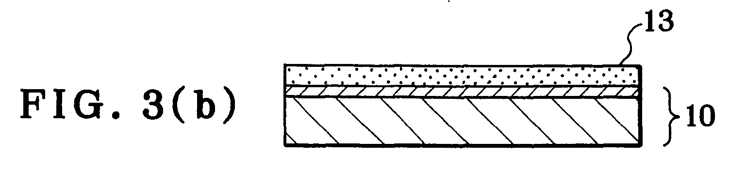
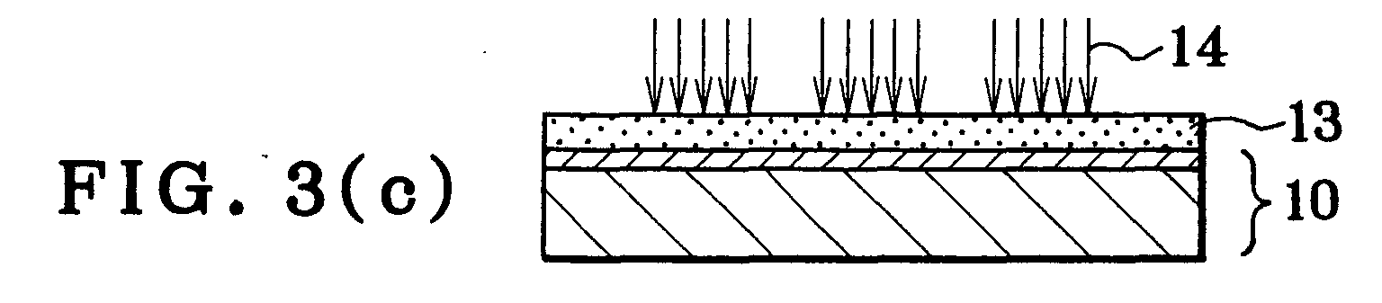
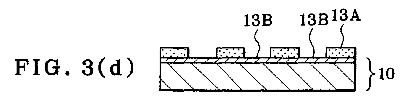
- Figs. 3(a) through 3(h) One specific process for etching a mask blank on the basis of the compiled writing data formed as explained above, thereby fabricating a phase mask is explained with reference to Figs. 3(a) through 3(h), wherein 10 stand for a phase mask blank, 11 a quartz substrate, 12 an opening in a chromium thin film, 13 an electron beam resist, 13A a resist pattern, 13B an opening in the resist, 14 an electron beam, 21 a phase mask, 26 a groove and 27 a strip.
- a mask blank 10 comprising a quartz substrate 11 and a 150 ⁇ -thick chromium thin film 12 formed by sputtering thereon.
- the chromium thin film 12 is helpful to prevent charging-up of an electron beam resist 13 upon irradiation with electron beams at the post-step, and severs as a mask upon grooves 26 formed in a quartz substrate 11. It is here noted that control of the thickness of the chromium thin film is of importance in view of resolution on chromium thin film etching, and so that thickness should be appropriately in the range of 100 to 200 ⁇ .
- RE5100P (Hitachi Chemical Industries Co., Ltd.) is coated as an electron beam resist 13 at a thickness of 400 nm, followed by drying.
- the electron beam resist 13 is exposed to light at an exposure of 1.2 ⁇ C/cm 2 using a raster scan type electron beam lithography device MEBES111 (made by ETEC Co., Ltd.) while the width of electron beams 14 between scanning lines is sequentially controlled on the basis of the compiled exposure data as already explained with reference to Fig. 2.
- MEBES111 made by ETEC Co., Ltd.
- PEB post exposure baking
- TMAH tetramethylammonium hydroxide
- etching of just 240 nm in depth is carried out using CF 4 gas, as shown in Fig. 3(f).
- Depth control is effected by control of etching time, so that etching is feasible with the depth range of 200 to 400 nm.
- the etching conditions are determined in such a way that the phase of excimer laser 23 that is exposure light is modulated by ⁇ radian.
- the resist pattern 13A is stripped with sulfuric acid at 70°C, after which, as shown in Fig. 3(h), the chromium thin film pattern 12A is etched out in an ammonium solution of ceric nitrate. Finally, rinsing is carried out to complete a line (strip 27)-to-space (groove 26) phase mask 21 which has a depth of 240 nm and a pitch changing linearly from 0.85 ⁇ m to 1.25 ⁇ m in the direction at right angles with the groove 26.
- phase mask obtained as mentioned above there no stitching error due to writing.
- a grating replicated using this phase mask is found to have improved group delay characteristics.
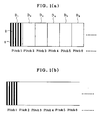
- Figs. 6(a) and 6(b) show the group delay and group delay ripple of a phase mask fabricated by a conventional process using an electron beam lithography system.
- Fig. 6(a) is a frequency vs. relative group delay graph
- Fig. 6(b) is a frequency vs. group delay ripple graph
- Figs. 7(a) and 7(b) show the group delay and group delay ripple of a phase mask fabricated by the writing process of the invention.
- Fig. 7(a) is a frequency vs. relative group delay graph
- Fig. 7(b) is a frequency vs. group delay ripple graph.
- a reduced delay ripple having a value smaller than that in the prior art.
- the present invention is not limited to the writing process for arranging pattern data in a row as shown in Fig. 2; that is, it may also be applied to writing processes for arranging pattern data in rows and columns.
- ripples can be much more reduced by forming a grating form of repetitive groove-and-strip pattern by multiple exposure.
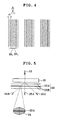
- FIG. 4 Multiple exposure may be carried out by multiple writing at the same place or arbitrarily displacing a writing area as shown in Fig. 4.
- reference numeral 26 1 represents a portion of one of adjacent segments wherein a groove is written and exposed to light (a solid line), and 26 2 stands for a portion of the other wherein a groove is written and exposed to light (a broken line).
- ⁇ be indicative of a displacement that occurs between adjacent segments.
- one groove is defined by an overlap of the exposed areas 26 1 and 26 2 , with the center being displaced by ⁇ /2 from the center of a groove having no overlap. In other words, that displacement is half that between writing areas; so stitching errors are reduced to half.
- the number of stitching errors is equal to the number of such operations.
- a raster scan type electron beam lithography device is used as the electron beam lithography device in the aforesaid fabrication process of the invention, it is understood that other writing devices inclusive of a vector scan type writing device may be used.
- one surface of a quartz substrate is irradiated with ultraviolet laser light, e.g., KrF excimer laser light of 248 nm wavelength via a phase mask 21 fabricated by the fabrication process of the invention to form a grating in a core 22A of an optical fiber 22 comprising a core 22A and a clad 22B, thereby preparing an optical fiber with a Bragg grating.
- ultraviolet laser light e.g., KrF excimer laser light of 248 nm wavelength
- the depth D (a difference in height between the strip 27 and the groove 26) of the groove 26 in the phase mask 21 fabricated by the fabrication process of the invention is selected such that the phase of excimer laser light 23 that is exposure light is modulated by ⁇ radian.
- light 25A of zero order is reduced by the phase mask 21 down to 5% or lower, and chief light laving the phase mask 21 is split into diffracted light 25B of plus first order, including 35% or more of diffracted light, and diffracted light 25C of minus first order.
- the thus obtained Bragg grating of the invention has group delay ripple characteristics of preferably ⁇ 10 ps or lower, and more preferably ⁇ 10 ps or lower.
- the Bragg grating fabricated by the fabrication process of the invention may be used to form a dispersion compensating module.
- the dispersion compensating module may be constructed by connecting a chirped Bragg grating to the second port of, for instance, a three-port type optical circulator. Input light is entered into the first port and output light leaves the third port. By imparting a temperature gradient to the chirped Bragg grating, the chirp rate (dispersion) may be controlled.
- a dispersion compensating device formed with a Bragg grating using the phase mask fabricated by the fabrication process of the invention is reduced in terms of group delay ripple and improved in terms of dispersion compensating function.
- writing data obtained by arranging and compiling a plurality of data for a repetitive groove-and-strip pattern while the pitch of repetition is modulated are used and an electron beam resist is provided on a phase mask blank, so that writing is carried out all over the writing area on said phase mask blank continuously in the direction vertical to the grating form of grooves, so that stitching errors on writing can be reduced to improve the group delay characteristics of a replicated Bragg grating.
- the phase mask of the invention has also the feature of being reduced in terms of stitching errors on writing.
- the optical fiber with a Bragg grating of the invention has improved group delay characteristics. Owing to reduced stitching errors, there are no unnecessary peaks on both sides of a Bragg peak.
- the dispersion compensating device of the invention has a reduced group delay ripple amplitude and an improved dispersion compensation function.
Landscapes
- Physics & Mathematics (AREA)
- General Physics & Mathematics (AREA)
- Diffracting Gratings Or Hologram Optical Elements (AREA)
- Optical Fibers, Optical Fiber Cores, And Optical Fiber Bundles (AREA)
- Preparing Plates And Mask In Photomechanical Process (AREA)
Abstract




Description
Claims (20)
- A process for the fabrication of a chirped type optical fiber-processing phase mask wherein a grating form of grooves provided in one surface of a quartz substrate is configured as an optical fiber-processing grating pattern, characterized in that:at an exposure step, writing data obtained by arranging and compiling a plurality of data for a repetitive groove-and-strip pattern while the pitch of repetition is modulated are used and an electron beam resist is provided on a phase mask blank, so that writing is carried out all over the writing area on said phase mask blank continuously in a vertical direction to said grating form of grooves.
- The process for the fabrication of an optical fiber-processing phase mask according to claim 1, characterized in that said grating form of repetitive groove-and-strip pattern is formed by multiple exposure.
- The process for the fabrication of an optical fiber-processing phase mask according to claim 2, characterized in that said multiple exposure is carried out by multiple writing at the same place.
- The process for the fabrication of an optical fiber-processing phase mask according to claim 2, characterized in that said multiple exposure is carried out by multiple writing at an arbitrarily displaced writing area.
- The process according to any one of claims 1 to 4, characterized in that writing is carried out by means of an electron beam lithography device.
- The process according to any one of claims 1 to 4, characterized in that writing is carried out by means of a laser light lithography device.
- The process according to any one of claims 1 to 6, characterized in that said grating form of repetitive groove-and-strip pattern has a pitch in the range of 0.85 µm to 1.25 µm.
- The process according to any one of claims 1 to 7, characterized in that a difference between a groove and a strip in said grating form of repetitive groove-and-strip pattern is of such magnitude that the phase of optical fiber-processing ultraviolet is shifted by about π upon transmission.
- A chirped type optical fiber-processing phase mask wherein a grating form of grooves provided in one surface of a quartz substrate is configured as an optical fiber-processing grating pattern, characterized in that:said phase mask is obtained by a fabrication process wherein at an exposure step, writing data obtained by arranging and compiling a plurality of data for a repetitive groove-and-strip pattern while the pitch of repetition is modulated are used and an electron beam resist is provided on a phase mask blank, so that writing is carried out all over the writing area on said phase mask blank continuously in a vertical direction to said grating form of grooves.
- The optical fiber-processing phase mask according to claim 9, characterized in that said grating form of repetitive groove-and-strip pattern is formed by multiple exposure.
- The optical fiber-processing phase mask according to claim 10, characterized in that said multiple exposure is carried out by multiple writing at the same place.
- The optical fiber-processing phase mask according to claim 10, characterized in that said multiple exposure is carried out by multiple writing at an arbitrarily displaced writing area.
- The phase mask according to any one of claims 9 to 12, wherein writing is carried out by means of an electron beam lithography device.
- The phase mask according to any one of claims 9 to 12, wherein writing is carried out by means of a laser light lithography device.
- The phase mask according to any one of claims 9 to 14, wherein said grating form of repetitive groove-and-strip pattern has a pitch in the range of 0.85 µm to 1.25 µm.
- The phase mask according to any one of claims 9 to 15, wherein a difference between a groove and a strip in said grating form of repetitive groove-and-strip pattern is of such magnitude that the phase of optical fiber-processing ultraviolet is shifted by about π upon transmission.
- An optical fiber with a Bragg grating, characterized in that:a phase mask according to any one of claims 9 to 16 or fabricated by the fabrication process of any one of claims 1 to 8 is used to process an optical fiber.
- The optical fiber with a Bragg grating according to claim 17, characterized by having group delay ripple characteristics of ±10 ps or lower.
- The optical fiber with a Bragg grating according to claim 17, characterized by having group delay ripple characteristics of ±3 ps or lower.
- A dispersion compensating device, which comprises a grating processed using a phase mask according to any one of claims 9 to 16 or fabricated by the fabrication process of any one of claims 1 to 8.
Applications Claiming Priority (2)
| Application Number | Priority Date | Filing Date | Title |
|---|---|---|---|
| JP2001265230 | 2001-09-03 | ||
| JP2001265230A JP3816769B2 (en) | 2001-09-03 | 2001-09-03 | Manufacturing method of optical fiber processing phase mask, optical fiber processing phase mask, optical fiber with Bragg grating, and dispersion compensation device using the optical fiber |
Publications (2)
| Publication Number | Publication Date |
|---|---|
| EP1288718A2 true EP1288718A2 (en) | 2003-03-05 |
| EP1288718A3 EP1288718A3 (en) | 2003-10-15 |
Family
ID=19091728
Family Applications (1)
| Application Number | Title | Priority Date | Filing Date |
|---|---|---|---|
| EP02019733A Withdrawn EP1288718A3 (en) | 2001-09-03 | 2002-09-03 | Process for the fabrication of a phase mask for optical fiber processing, optical fiber-processing phase mask, optical fiber with bragg grating, and dispersion compensation device using the optical fiber |
Country Status (4)
| Country | Link |
|---|---|
| US (1) | US7153613B2 (en) |
| EP (1) | EP1288718A3 (en) |
| JP (1) | JP3816769B2 (en) |
| CA (1) | CA2401111C (en) |
Cited By (1)
| Publication number | Priority date | Publication date | Assignee | Title |
|---|---|---|---|---|
| EP2403076A3 (en) * | 2003-06-03 | 2014-08-06 | Imra America, Inc. | In-line, high energy fiber chirped pulse amplification system |
Families Citing this family (12)
| Publication number | Priority date | Publication date | Assignee | Title |
|---|---|---|---|---|
| US6829067B2 (en) * | 2000-12-04 | 2004-12-07 | California Institute Of Technology | Method and apparatus for implementing a multi-channel tunable filter |
| KR100575230B1 (en) * | 2002-12-28 | 2006-05-02 | 엘지.필립스 엘시디 주식회사 | Exposure method using exposure apparatus |
| US8320722B1 (en) * | 2010-04-13 | 2012-11-27 | Western Digital (Fremont), Llc | Non-linear optical grating |
| US8422841B1 (en) | 2010-05-13 | 2013-04-16 | Western Digital (Fremont), Llc | Double optical grating |
| JP5887833B2 (en) * | 2011-10-28 | 2016-03-16 | 大日本印刷株式会社 | Optical fiber processing phase mask and manufacturing method thereof |
| CN102520482A (en) * | 2011-12-19 | 2012-06-27 | 深圳市易飞扬通信技术有限公司 | Critical method for manufacturing fiber array by semiconductor technology |
| KR102002958B1 (en) * | 2012-09-04 | 2019-07-24 | 삼성디스플레이 주식회사 | Patterning mask |
| KR102612412B1 (en) * | 2016-02-05 | 2023-12-12 | 한국전자통신연구원 | Imaging sensor and method of manufacturing the same |
| US10534115B1 (en) * | 2017-09-22 | 2020-01-14 | Facebook Technologies, Llc | Gray-tone electron-beam lithography |
| US11220028B1 (en) | 2018-03-08 | 2022-01-11 | Facebook Technologies, Llc | Method of manufacture for thin, multi-bend optics by compression molding |
| US10976483B2 (en) | 2019-02-26 | 2021-04-13 | Facebook Technologies, Llc | Variable-etch-depth gratings |
| US11709422B2 (en) | 2020-09-17 | 2023-07-25 | Meta Platforms Technologies, Llc | Gray-tone lithography for precise control of grating etch depth |
Family Cites Families (8)
| Publication number | Priority date | Publication date | Assignee | Title |
|---|---|---|---|---|
| US5413884A (en) * | 1992-12-14 | 1995-05-09 | American Telephone And Telegraph Company | Grating fabrication using electron beam lithography |
| US5327515A (en) * | 1993-01-14 | 1994-07-05 | At&T Laboratories | Method for forming a Bragg grating in an optical medium |
| GB9509874D0 (en) * | 1995-05-16 | 1995-07-12 | Univ Southampton | Optical waveguide grating |
| JPH0980738A (en) * | 1995-09-07 | 1997-03-28 | Dainippon Printing Co Ltd | Manufacturing method of phase shift photomask for optical fiber processing |
| JP3526215B2 (en) * | 1997-07-03 | 2004-05-10 | 大日本印刷株式会社 | Phase mask for optical fiber processing and method of manufacturing the same |
| JPH1184623A (en) * | 1997-09-03 | 1999-03-26 | Dainippon Printing Co Ltd | Method of manufacturing phase mask for optical fiber processing and optical fiber with Bragg diffraction grating manufactured using the phase mask for optical fiber processing |
| US20020028390A1 (en) * | 1997-09-22 | 2002-03-07 | Mohammad A. Mazed | Techniques for fabricating and packaging multi-wavelength semiconductor laser array devices (chips) and their applications in system architectures |
| JP2001242313A (en) * | 2000-02-28 | 2001-09-07 | Dainippon Printing Co Ltd | Method of manufacturing phase mask for optical fiber processing and optical fiber with Bragg diffraction grating manufactured using the phase mask for optical fiber processing |
-
2001
- 2001-09-03 JP JP2001265230A patent/JP3816769B2/en not_active Expired - Lifetime
-
2002
- 2002-09-03 CA CA2401111A patent/CA2401111C/en not_active Expired - Lifetime
- 2002-09-03 EP EP02019733A patent/EP1288718A3/en not_active Withdrawn
- 2002-09-03 US US10/234,452 patent/US7153613B2/en not_active Expired - Lifetime
Cited By (1)
| Publication number | Priority date | Publication date | Assignee | Title |
|---|---|---|---|---|
| EP2403076A3 (en) * | 2003-06-03 | 2014-08-06 | Imra America, Inc. | In-line, high energy fiber chirped pulse amplification system |
Also Published As
| Publication number | Publication date |
|---|---|
| JP2003075620A (en) | 2003-03-12 |
| CA2401111A1 (en) | 2003-03-03 |
| US20030077039A1 (en) | 2003-04-24 |
| CA2401111C (en) | 2010-07-06 |
| US7153613B2 (en) | 2006-12-26 |
| JP3816769B2 (en) | 2006-08-30 |
| EP1288718A3 (en) | 2003-10-15 |
Similar Documents
| Publication | Publication Date | Title |
|---|---|---|
| CA2264843C (en) | Phase mask for machining optical fibers, and its fabrication method | |
| US7153613B2 (en) | Process for the fabrication of a phase mask for optical fiber processing, optical fiber-processing phase mask, optical fiber with a Bragg grating, and dispersion compensating device using the optical fiber | |
| US5760960A (en) | Cascaded self-induced holography | |
| US20030107787A1 (en) | Planar and fiber optical apodized diffraction structures fabrication | |
| JPH10142413A (en) | Production of continuously chirped phase mask | |
| US5953471A (en) | Optical communication system having short period reflective Bragg gratings | |
| US5730888A (en) | Bragg gratings in waveguides | |
| US6795614B2 (en) | Method of making phase mask for machining optical fiber and optical fiber having bragg diffraction grating produced using the phase mask for machining optical fiber | |
| US6466714B1 (en) | Method of producing phase mask for fabricating optical fiber and optical fiber with bragg's diffraction grating produced by using the phase mask | |
| Komukai et al. | Group delay ripple reduction and reflectivity increase in a chirped fiber Bragg grating by multiple-overwriting of a phase mask with an electron-beam | |
| US6876792B2 (en) | Phase mask for forming diffraction grating, and optical fiber and optical waveguide having diffraction grating duplicated using the phase mask | |
| JP3693494B2 (en) | Chirped optical fiber filter manufacturing method and chirped optical fiber filter | |
| US20030108802A1 (en) | Planar and fiber optical grating structures fabrication apparatus and method | |
| US20030107786A1 (en) | Precision optical apparatus utilizing non-optically smooth material | |
| US7081323B2 (en) | Method of making gratings and phase masks for fiber grating fabrication | |
| CA2580820C (en) | Phase mask for processing optical fibers, and its fabrication method | |
| JPH11223714A (en) | Phase mask for manufacturing diffraction grating and method for manufacturing the same | |
| JP3818518B2 (en) | Manufacturing method of phase mask for optical fiber processing | |
| JP4668696B2 (en) | Method for producing chirped grating forming substrate | |
| JPH0344601A (en) | Production of grating | |
| JPH02253203A (en) | How to make grating | |
| HU225575B1 (en) | Method of manufacturing an integrated optical element and wavelength selective element on wavelength divison multiplexer systems |
Legal Events
| Date | Code | Title | Description |
|---|---|---|---|
| PUAI | Public reference made under article 153(3) epc to a published international application that has entered the european phase |
Free format text: ORIGINAL CODE: 0009012 |
|
| AK | Designated contracting states |
Kind code of ref document: A2 Designated state(s): AT BE BG CH CY CZ DE DK EE ES FI FR GB GR IE IT LI LU MC NL PT SE SK TR Designated state(s): AT BE BG CH CY CZ DE DK EE ES FI FR GB GR IE IT LI LU MC NL PT SE SK TR |
|
| AX | Request for extension of the european patent |
Extension state: AL LT LV MK RO SI |
|
| PUAL | Search report despatched |
Free format text: ORIGINAL CODE: 0009013 |
|
| AK | Designated contracting states |
Kind code of ref document: A3 Designated state(s): AT BE BG CH CY CZ DE DK EE ES FI FR GB GR IE IT LI LU MC NL PT SE SK TR |
|
| AX | Request for extension of the european patent |
Extension state: AL LT LV MK RO SI |
|
| RIC1 | Information provided on ipc code assigned before grant |
Ipc: 7G 03F 7/20 B Ipc: 7G 03F 1/14 B Ipc: 7G 02B 6/16 A |
|
| 17P | Request for examination filed |
Effective date: 20040318 |
|
| AKX | Designation fees paid |
Designated state(s): DE FR GB |
|
| 17Q | First examination report despatched |
Effective date: 20040527 |
|
| 17Q | First examination report despatched |
Effective date: 20040527 |
|
| STAA | Information on the status of an ep patent application or granted ep patent |
Free format text: STATUS: THE APPLICATION HAS BEEN WITHDRAWN |
|
| 18W | Application withdrawn |
Effective date: 20080912 |