EP1286575A2 - Module component, core substrate element assembly, multi-layer substrate, method of manufacturing core substrate element assembly, method of manufacturing multi-layer substrate, and method of manufacturing module component - Google Patents
Module component, core substrate element assembly, multi-layer substrate, method of manufacturing core substrate element assembly, method of manufacturing multi-layer substrate, and method of manufacturing module component Download PDFInfo
- Publication number
- EP1286575A2 EP1286575A2 EP02255550A EP02255550A EP1286575A2 EP 1286575 A2 EP1286575 A2 EP 1286575A2 EP 02255550 A EP02255550 A EP 02255550A EP 02255550 A EP02255550 A EP 02255550A EP 1286575 A2 EP1286575 A2 EP 1286575A2
- Authority
- EP
- European Patent Office
- Prior art keywords
- layer
- sheet
- core
- module component
- element assembly
- Prior art date
- Legal status (The legal status is an assumption and is not a legal conclusion. Google has not performed a legal analysis and makes no representation as to the accuracy of the status listed.)
- Withdrawn
Links
Images






Classifications
-
- H—ELECTRICITY
- H05—ELECTRIC TECHNIQUES NOT OTHERWISE PROVIDED FOR
- H05K—PRINTED CIRCUITS; CASINGS OR CONSTRUCTIONAL DETAILS OF ELECTRIC APPARATUS; MANUFACTURE OF ASSEMBLAGES OF ELECTRICAL COMPONENTS
- H05K1/00—Printed circuits
- H05K1/02—Details
- H05K1/03—Use of materials for the substrate
- H05K1/0313—Organic insulating material
- H05K1/0353—Organic insulating material consisting of two or more materials, e.g. two or more polymers, polymer + filler, + reinforcement
- H05K1/0366—Organic insulating material consisting of two or more materials, e.g. two or more polymers, polymer + filler, + reinforcement reinforced, e.g. by fibres, fabrics
-
- H—ELECTRICITY
- H05—ELECTRIC TECHNIQUES NOT OTHERWISE PROVIDED FOR
- H05K—PRINTED CIRCUITS; CASINGS OR CONSTRUCTIONAL DETAILS OF ELECTRIC APPARATUS; MANUFACTURE OF ASSEMBLAGES OF ELECTRICAL COMPONENTS
- H05K3/00—Apparatus or processes for manufacturing printed circuits
- H05K3/46—Manufacturing multilayer circuits
-
- H—ELECTRICITY
- H05—ELECTRIC TECHNIQUES NOT OTHERWISE PROVIDED FOR
- H05K—PRINTED CIRCUITS; CASINGS OR CONSTRUCTIONAL DETAILS OF ELECTRIC APPARATUS; MANUFACTURE OF ASSEMBLAGES OF ELECTRICAL COMPONENTS
- H05K1/00—Printed circuits
- H05K1/02—Details
- H05K1/0271—Arrangements for reducing stress or warp in rigid printed circuit boards, e.g. caused by loads, vibrations or differences in thermal expansion
-
- H—ELECTRICITY
- H05—ELECTRIC TECHNIQUES NOT OTHERWISE PROVIDED FOR
- H05K—PRINTED CIRCUITS; CASINGS OR CONSTRUCTIONAL DETAILS OF ELECTRIC APPARATUS; MANUFACTURE OF ASSEMBLAGES OF ELECTRICAL COMPONENTS
- H05K3/00—Apparatus or processes for manufacturing printed circuits
- H05K3/46—Manufacturing multilayer circuits
- H05K3/4602—Manufacturing multilayer circuits characterized by a special circuit board as base or central core whereon additional circuit layers are built or additional circuit boards are laminated
-
- H—ELECTRICITY
- H05—ELECTRIC TECHNIQUES NOT OTHERWISE PROVIDED FOR
- H05K—PRINTED CIRCUITS; CASINGS OR CONSTRUCTIONAL DETAILS OF ELECTRIC APPARATUS; MANUFACTURE OF ASSEMBLAGES OF ELECTRICAL COMPONENTS
- H05K1/00—Printed circuits
- H05K1/02—Details
- H05K1/03—Use of materials for the substrate
- H05K1/0313—Organic insulating material
- H05K1/0353—Organic insulating material consisting of two or more materials, e.g. two or more polymers, polymer + filler, + reinforcement
- H05K1/036—Multilayers with layers of different types
-
- H—ELECTRICITY
- H05—ELECTRIC TECHNIQUES NOT OTHERWISE PROVIDED FOR
- H05K—PRINTED CIRCUITS; CASINGS OR CONSTRUCTIONAL DETAILS OF ELECTRIC APPARATUS; MANUFACTURE OF ASSEMBLAGES OF ELECTRICAL COMPONENTS
- H05K2201/00—Indexing scheme relating to printed circuits covered by H05K1/00
- H05K2201/01—Dielectrics
- H05K2201/0183—Dielectric layers
- H05K2201/0187—Dielectric layers with regions of different dielectrics in the same layer, e.g. in a printed capacitor for locally changing the dielectric properties
-
- H—ELECTRICITY
- H05—ELECTRIC TECHNIQUES NOT OTHERWISE PROVIDED FOR
- H05K—PRINTED CIRCUITS; CASINGS OR CONSTRUCTIONAL DETAILS OF ELECTRIC APPARATUS; MANUFACTURE OF ASSEMBLAGES OF ELECTRICAL COMPONENTS
- H05K2201/00—Indexing scheme relating to printed circuits covered by H05K1/00
- H05K2201/02—Fillers; Particles; Fibers; Reinforcement materials
- H05K2201/0203—Fillers and particles
- H05K2201/0206—Materials
- H05K2201/0209—Inorganic, non-metallic particles
-
- H—ELECTRICITY
- H05—ELECTRIC TECHNIQUES NOT OTHERWISE PROVIDED FOR
- H05K—PRINTED CIRCUITS; CASINGS OR CONSTRUCTIONAL DETAILS OF ELECTRIC APPARATUS; MANUFACTURE OF ASSEMBLAGES OF ELECTRICAL COMPONENTS
- H05K2201/00—Indexing scheme relating to printed circuits covered by H05K1/00
- H05K2201/09—Shape and layout
- H05K2201/09818—Shape or layout details not covered by a single group of H05K2201/09009 - H05K2201/09809
- H05K2201/09909—Special local insulating pattern, e.g. as dam around component
-
- H—ELECTRICITY
- H05—ELECTRIC TECHNIQUES NOT OTHERWISE PROVIDED FOR
- H05K—PRINTED CIRCUITS; CASINGS OR CONSTRUCTIONAL DETAILS OF ELECTRIC APPARATUS; MANUFACTURE OF ASSEMBLAGES OF ELECTRICAL COMPONENTS
- H05K2201/00—Indexing scheme relating to printed circuits covered by H05K1/00
- H05K2201/20—Details of printed circuits not provided for in H05K2201/01 - H05K2201/10
- H05K2201/2009—Reinforced areas, e.g. for a specific part of a flexible printed circuit
-
- H—ELECTRICITY
- H05—ELECTRIC TECHNIQUES NOT OTHERWISE PROVIDED FOR
- H05K—PRINTED CIRCUITS; CASINGS OR CONSTRUCTIONAL DETAILS OF ELECTRIC APPARATUS; MANUFACTURE OF ASSEMBLAGES OF ELECTRICAL COMPONENTS
- H05K2203/00—Indexing scheme relating to apparatus or processes for manufacturing printed circuits covered by H05K3/00
- H05K2203/06—Lamination
- H05K2203/061—Lamination of previously made multilayered subassemblies
-
- H—ELECTRICITY
- H05—ELECTRIC TECHNIQUES NOT OTHERWISE PROVIDED FOR
- H05K—PRINTED CIRCUITS; CASINGS OR CONSTRUCTIONAL DETAILS OF ELECTRIC APPARATUS; MANUFACTURE OF ASSEMBLAGES OF ELECTRICAL COMPONENTS
- H05K2203/00—Indexing scheme relating to apparatus or processes for manufacturing printed circuits covered by H05K3/00
- H05K2203/06—Lamination
- H05K2203/065—Binding insulating layers without adhesive, e.g. by local heating or welding, before lamination of the whole PCB
-
- H—ELECTRICITY
- H05—ELECTRIC TECHNIQUES NOT OTHERWISE PROVIDED FOR
- H05K—PRINTED CIRCUITS; CASINGS OR CONSTRUCTIONAL DETAILS OF ELECTRIC APPARATUS; MANUFACTURE OF ASSEMBLAGES OF ELECTRICAL COMPONENTS
- H05K3/00—Apparatus or processes for manufacturing printed circuits
- H05K3/0011—Working of insulating substrates or insulating layers
- H05K3/0044—Mechanical working of the substrate, e.g. drilling or punching
- H05K3/0052—Depaneling, i.e. dividing a panel into circuit boards; Working of the edges of circuit boards
-
- H—ELECTRICITY
- H05—ELECTRIC TECHNIQUES NOT OTHERWISE PROVIDED FOR
- H05K—PRINTED CIRCUITS; CASINGS OR CONSTRUCTIONAL DETAILS OF ELECTRIC APPARATUS; MANUFACTURE OF ASSEMBLAGES OF ELECTRICAL COMPONENTS
- H05K3/00—Apparatus or processes for manufacturing printed circuits
- H05K3/46—Manufacturing multilayer circuits
- H05K3/4644—Manufacturing multilayer circuits by building the multilayer layer by layer, i.e. build-up multilayer circuits
- H05K3/4652—Adding a circuit layer by laminating a metal foil or a preformed metal foil pattern
-
- H—ELECTRICITY
- H10—SEMICONDUCTOR DEVICES; ELECTRIC SOLID-STATE DEVICES NOT OTHERWISE PROVIDED FOR
- H10W—GENERIC PACKAGES, INTERCONNECTIONS, CONNECTORS OR OTHER CONSTRUCTIONAL DETAILS OF DEVICES COVERED BY CLASS H10
- H10W72/00—Interconnections or connectors in packages
- H10W72/01—Manufacture or treatment
- H10W72/0198—Manufacture or treatment batch processes
Definitions
- the present invention relates to a module component, a core substrate element assembly, a multi-layer substrate, a method of manufacturing a core substrate element assembly, a method of manufacturing a multi-layer substrate, and a method of manufacturing a module component
- the multi-layer substrate disclosed in Japanese Patent Publication No. 1996-139424A is manufactured by first preparing a glass cloth formed by weaving a large number of glass fiber bundles in a lattice shape, and a work sheet comprising this glass cloth impregnated with a synthetic resin, and then dividing this work sheet in a direction intersecting the glass fiber bundles to form individual pieces. Because the multi-layer substrate is manufactured by dividing the work sheet in a direction intersecting the glass fiber bundles, the resulting structure is such that the cut surfaces of the glass cloth and the synthetic resin are exposed at the sides of the multi-layer substrate.
- the adhesiveness of the glass cloth to the synthetic resin is low.
- the structure in which the cut surfaces of the glass cloth and the synthetic resin are exposed at the sides of the multi-layer substrate as in Japanese Patent Publication No. 1996-139424A there is a problem that moisture in the air is absorbed into the multi-layer substrate from the interfaces between the glass cloth and the synthetic resin, resulting in a degradation of electrical properties such as insulation.
- the glass cloth has a structure in which a large number of glass fibers are bundled together, and hence there are cavities between the glass fibers in a number corresponding to the number of glass fibers. There are thus a large number of cavities at the cut surfaces of the glass cloth, and hence there is a problem that a large amount of moisture in the air is absorbed into the multi-layer substrate from these cavities, resulting in a marked degradation of electrical properties such as insulation.
- the module component according to the present invention comprises an intermediate layer, an upper layer, a lower layer and a mounted component.
- the intermediate layer comprises a first layer, a second layer, and a core layer.
- the core layer comprises a material having a higher strength than the first layer and the second layer, has a network structure that extends out in planar fashion, has an outer periphery thereof positioned further to the inside than the outer peripheries of the first layer and the second layer, and is sealed between the first layer and the second layer.
- the upper layer is laminated on an upper surface of the intermediate layer.
- the lower layer is laminated on a lower surface of the intermediate layer.
- the mounted component is mounted on any one of the upper layer and the lower layer.
- the core layer comprises a material having a higher strength than the first layer and the second layer, and extends out in planar fashion. As a result, the strength in a direction orthogonal to the principal plane ofthe core layer is increased.
- the core layer is sealed between the first layer and the second layer, and hence the first layer, the second layer and the core layer are integrated into a single body.
- the module component according to the present invention has increased strength in the direction orthogonal to the principal plane of the core layer. Accordingly, the strength required of the intermediate layer of the module component can be secured.
- the outer periphery of the core layer is positioned further to the inside than the outer peripheries of the first layer and the second layer.
- the core layer has a network structure, and hence the first layer and the second layer are bonded together via the gaps in the network structure.
- the core layer has a network structure, and hence the first layer and the second layer are bonded together via the gaps in the network structure.
- the core layer is sealed between the first layer and the second layer, and hence is not exposed to the outside.
- the upper layer is laminated on the upper surface of the intermediate layer
- the lower layer is laminated on the lower surface of the intermediate layer, and hence the upper layer and the lower layer are integrated into a single body via the intermediate layer.
- any chosen material can be used for the upper layer and the lower layer, and any chosen circuit elements can be constituted in the upper layer and the lower layer.
- the mounted component is mounted on any one of the upper layer and the lower layer.
- circuit elements formed in any one of the intermediate layer, the upper layer and the lower layer are integrated with the mounted component, and hence functions as a module component can be exhibited.
- a method of manufacturing a module component as described above, a core substrate element assembly and a multi-layer substrate suitable for manufacturing such a module component and methods of manufacturingsuch a core substrate element assembly and such a multi-layer substrate.
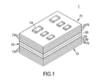
- the module component 1 comprises an intermediate layer 70, an upper layer 71, a lower layer 72 and mounted components 74.
- the intermediate layer 70 which is a substrate constituting the core of the module component, comprises a first layer 20, a second layer 30, a core layer 10, conductive patterns 41, 42 and 50, and through holes 60.
- the core layer 10 comprises a material having a higher strength than the first layer 20 and the second layer 30, and has a network structure that extends out in planar fashion.
- the core layer 10 comprises, for example, a ceramic component and a first thermosetting resin mixed together.
- the ceramic component preferably comprises at least one member selected from the group consisting of glass type ceramics, alumina type ceramics and quartz.
- the first thermosetting resin preferably comprises at least one member selected from the group consisting of epoxy resins, phenol resins, BT resins (Bismaleimide-Triazine reins), polyimide resins andvinylbenzyl resins.
- resin materials for the first layer 20 and the second layer 30 that have high adhesiveness to one another.
- resin materials that have high adhesiveness to one another can be constituted.
- resins having different composition to one another may be used for the first layer 20 and the second layer 30.
- the first layer 20 and the second layer 30 can comprise a resin or a hybrid material, and the hybrid material can be formed by mixing a resin with any one of ceramics, dielectric materials and magnetic materials.
- the resin preferably comprises at least one member selected from the group consisting of epoxy resins, phenol resins, BT resins, PPE (PolyPhenyleneEther), PPO (PolyPhenyleneOxide), polyimide resins and vinylbenzyl resins.
- the ceramic component preferably comprises at least one member selected from the group consisting of glass type ceramics, alumina type ceramics, forsterite type ceramics, barium titanate type ceramics, BaTiO 3 -BaZrO 3 type ceramics, BaO-TiO 2 -Nd 2 O 3 type ceramics and BaO-4TiO 2 type ceramics
- the resin preferably comprises at least one member selected from the consisting of epoxy resins, phenol resins, BT resins, PPE, PPO, polyimide resins and vinylbenzyl resins.
- thermosetting resin is used for the first layer 20 and the second layer 30.
- This second thermosetting resin is the resin material having a higher thermosetting temperature than the first thermosetting resin.
- the second thermosetting resin for example, comprises at least one member selected from the group consisting of epoxy resins, phenol resins, BT resins, polyimide resins and vinylbenzyl resins.
- the core layer 10 is arranged so that the outer periphery 11 of the core layer 10 is positioned further to the inside than the outer peripheries of the first layer 20 and the second layer 30, and the core layer 10 is sealed between the first layer 20 and the second layer 30.
- the conductive patterns 41 and 42 are provided on the main surface of the second layer 30 on the side on which the core layer 10 is not provided.
- the conductive pattern 50 is provided on the main surface of the first layer 20 on the side on which the core layer 10 is not provided.
- the conductive patterns 41, 42 and 50 can be made to have any chosen shape. These conductive patterns 41, 42 and 50 constitute passive elements such as capacitors or coils, or wiring patterns.
- the through holes 60 are provided in the first layer 20 and the second layer 30, avoiding parts where the core layer 10 is disposed. Each of the through holes 60 is plated (the plating films are not shown in the drawings).
- the upper layer 71 and the lower layer 72 each comprises a plurality of circuit-forming layers 75 and conductive patterns 73, constituting circuit elements such as capacitors or coils.
- the circuit-forming layers 75 have an organic component as a principal component, and are laminated to one another.
- the conductive patterns 73 are provided between the circuit-forming layers 75.
- the upper layer 71 is laminated on an upper surface of the intermediate layer 70, and the lower layer 72 is laminated on a lower surface of the intermediate layer 70.
- Each mounted component 74 is, for example, a passive element such as a resistor, a capacitor or a coil, an active element such as a transistor, or an IC or the like.
- the mounted components 74 are disposed on the uppermost surface of the upper layer 71. Moreover, the mounted components 74 may also be disposed on the lower layer 72.
- the core layer 10 comprises a material having a higher strength than the first layer 20 and the second layer 30, and extends out in planar fashion. As a result, the strength in the direction orthogonal to the principal plane of the core layer 10 is increased.
- the core layer 10 is sealed between the first layer 20 and the second layer 30, and the first layer 20, the second layer 30 and the core layer 10 are integrated into a single body.
- the module component according to the present embodiment has increased strength in the direction orthogonal to the principal plane of the core layer 10. The strength required of the intermediate layer of the module component can thus be secured.
- the outer periphery 11 of the core layer 10 is positioned further to the inside than the outer peripheries of the first layer 20 and the second layer 30.
- the core layer 10 has a network structure, and hence the first layer 20 and the second layer 30 are bonded together via the gaps in the network structure.
- the strength of bonding between the first layer 20, the second layer 30 and the core layer 10 can be increased.
- the core layer 10 has a network structure, it is possible to form through holes avoiding the core layer 10.
- the core layer 10 is sealed between the first layer 20 and the second layer 30, and hence is not exposed to the outside.
- the adhesiveness of the first layer 20 and the second layer 30 to the core layer 10 is low, there will be no absorption of moisture in the air from the interfaces of the core layer 10, and hence degradation of the electrical properties of the circuit elements of the module component can be prevented.
- the upper layer 71 is laminated on the upper surface of the intermediate layer 70
- the lower layer 72 is laminated on the lower surface of the intermediate layer 70, and hence the upper layer 71 and the lower layer 72 are integrated into a single body via the intermediate layer 70.
- strength can be secured due to the intermediate layer 70, and hence even if the upper layer 71 and the lower layer 72 are not strong, the substrate strength of the module component as a whole can be secured.
- any chosen material can be used for the upper layer 71 and the lower layer 72, and any chosen circuit elements can be constituted in the upper layer 71 and the lower layer 72.
- the mounted components 74 are mounted on any one of the upper layer 71 and the lower layer 72.
- circuit elements formed in the intermediate layer 70, the upper layer 71 or the lower layer 72 are integrated with the mounted components 74, and hence functions as a module component 1 can be exhibited.
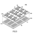
- the core substrate element assembly 400 comprises a first sheet 410, a second sheet 420, and a group of core layers 10.
- the first sheet 410 comprises a second thermosetting resin 200, conductive patterns 50, and through holes 60 (not shown).
- the second sheet 420 comprises the second thermosetting resin 200, conductive patterns 41 and 42, and through holes 60.
- the group of core layers 10 comprises a plurality of core layers 10 arranged with prescribed gaps there between.
- the second thermosetting resin is used for the first sheet 410 and the second sheet 420.
- the same material of which the first layer 20 and the second layer 30 are formed for example, the hybrid material formed by mixing a resin with any one of ceramics, dielectric material and magnetic material, may be used.
- the conductive patterns 50 are provided on the main surface of the second thermosetting resin 200 of the first sheet 410.
- the conductive patterns 41 and 42 are provided on the main surface of the second thermosetting resin 200 of the second sheet 420.
- the group of core layers 10 is disposed between the second thermosetting resin 200 of the first sheet 410 and the second thermosetting resin 200 of the second sheet 420.
- the core substrate element assembly 400 has a constitution in which intermediate layers 70 as shown in Fig. 1 are arranged in a continuous array. As a result, by cutting in the gaps between the core layers 10, for example along the alternate-dot-and-dash lines shown in Fig. 5, the intermediate layers 70 of module components 1 can be manufactured easily.
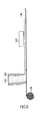
- firstly metal foil 100, a core layer material 331 in the form of a slurry, and the second thermosetting resin 200 in the form of a slurry are prepared.
- a suitable metal having a good electrical conductivity such as gold, silver, copper or aluminum is used as the metal foil 100.
- copper is particularly preferably.
- Any of various publicly-known methods such as electrolysis or rolling can be used as the method of manufacturing the metal foil 100, but in the case that one wishes to obtain good foil peeling strength, and one attaches importance to the high frequency characteristics of an electrolyzed foil, it is preferable to use a rolled foil for which skin effects due to surface unevenness are small.
- the core layer material 331 comprises a ceramic component and a first thermosetting resin mixed together.
- the slurry-form second thermosetting resin 200 is applied onto the metal foil 100, the thickness of the second thermosetting resin 200 is made uniform by using a doctor blade 300, and drying is carried out using a dryer 310.
- the dried second thermosetting resin 200 and metal foil 100 are cut using a dicer 320, thus forming the first sheet 410 and the second sheet 420.
- the first sheet 410 and the second sheet 420 have the same shape and structure, but sheets having a different shape and structure to one another may be used.
- the slurry-form core layer material 331 which has been fed to a screen printing plate 330, is extruded using a squeegee 332, thus printing the core layer material 331 with prescribed gaps, and hence forming the group of core layers 10.
- the group of core layers 10 and the first sheet 410 are heated and dried, thus hardening the core layers 10.
- the core layers 10 are arranged in an array of for example "n” rows and “m” columns ("n” and “m” are any chosen natural numbers), thus constituting a group.
- the main surface of the second sheet 420 on the side on which the second thermosetting resin 200 has been provided is placed on the main surface of the first sheet 410 on the side on which the core layers 10 have been provided, and pressure and heat are applied. As a result, the two pieces of the second thermosetting resin 200 are bonded together via the core layers 10 and are hardened.
- the heating temperature is, for example, about 200°C.
- the through holes 60 are formed through the first sheet 410 and the second sheet 420, avoiding the core layers 10.
- the through holes 60 formed are then plated (the plating films are not shown).
- a resist of a prescribed pattern is applied onto the metal foil 100, and etching is carried out, thus forming the conductive patterns 41, 42 and 50.
- the core substrate element assembly 400 according to the present invention can also be manufactured using a continuous coating method, but detailed description will not be given here.
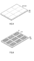
- the multi-layer substrate 2 according to the present embodiment comprises the core substrate element assembly 400, an upper sheet 710 and a lower sheet 720.
- the upper sheet 710 and the lower sheet 720 each comprises a plurality of circuit-forming sheets 750 and conductive patterns 73.
- the circuit-forming sheets 750 comprise the same material as the circuit-forming layers 75, and are laminated together.
- the conductive patterns 73 are provided between the circuit-forming sheets 750.
- the upper sheet 710 is laminated onto the upper surface of the core substrate element assembly 400, and the lower sheet 720 is laminated onto the lower surface of the core substrate element assembly 400.
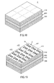
- the multi-layer substrate 2 has a structure in which module components 1 as shown in Fig. 1 are arranged in a continuous array. By cutting in the gaps between the core layers 10, for example along the alternate-dot-and-dash lines shown in Fig. 14, module components 1 can thus be manufactured easily.
- a circuit-forming sheet 750 is laminated onto each of the upper surface and the lower surface of the core substrate element assembly 400.
- conductive patterns 73 are formed on the circuit-forming sheets 750.
- other circuit-forming sheets 750 are laminated onto the circuit-forming sheets 750.
- a multi-layer substrate 2 and mounted components 74 are prepared.
- the mounted components 74 are mounted on the multi-layer substrate 2.
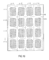
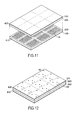
- the multi-layer substrate 2 is then cut in the gaps between the core layers 10, for example along the alternate-dot-and-dash lines shown in Fig. 19, thus manufacturing a plurality of module components 1. More specifically, as shown in Figs. 20 to 22, by cutting the multi-layer substrate 2 on which the mounted components 74 have been mounted along x11 and x12 in the transverse direction, and then along y21 and y22 in the longitudinal direction,the module components 1 can be manufactured.
- the method of manufacturing the module component 1 according to the present embodiment used the multi-layer substrate 2, and hence module components 1 having the same structure as one another can be mass-produced easily.
Landscapes
- Engineering & Computer Science (AREA)
- Microelectronics & Electronic Packaging (AREA)
- Manufacturing & Machinery (AREA)
- Production Of Multi-Layered Print Wiring Board (AREA)
- Laminated Bodies (AREA)
- Non-Metallic Protective Coatings For Printed Circuits (AREA)
Abstract
Description
Claims (16)
- A module component comprising an intermediate layer (70), an upper layer (71), a lower layer (72) and a mounted component (74) characterized in that:the intermediate layer (70) includes a first layer (20), a second layer (30) and a core layer (10);the core layer (10) comprises a material having a higher strength than the first layer (20) and the second layer (30), has a network structure that extends out in planar fashion, has an outer periphery thereof positioned further to the inside than outer peripheries of the first layer (20) and the second layer (30) and is sealed between the first layer (20) and the second layer (30);the upper layer (71) is laminated on an upper surface of the intermediate layer (70);the lower layer (72) is laminated on a lower surface of the intermediate layer (70); andthe mounted component (74) is mounted on any one of theupper layer (71) and the lower layer (72).
- The module component according to claim 1, wherein the core layer (10) comprises a mixture of a ceramic component and a first thermosetting resin
- The module component according to claim 2, wherein the ceramic component comprises at least one member selected fromthe group consisting of glass type ceramics, alumina type ceramics and quartz, and the first thermosetting resin comprises at least one member selected from the group consisting of epoxy resins, phenol resins, BT resins, polyimide resins and vinylbenzyl resins.
- The module component according to claim 1, wherein any one of the first layer (20) and the second layer (30) comprises a resin.
- The module component according to claim 4, wherein the resin comprises at least one member selected from the group consisting of epoxy resins, phenol resins, BT resins, PPE, PPO, polyimide resins and vinylbenzyl resins.
- The module component according to claim 2, wherein the first layer (20) and the second layer (30) each comprises a second thermosetting resin, and a thermosetting temperature of the second thermosetting resin is higher than a thermosetting temperature of the first thermosetting resin.
- The module component according to claim 1, wherein any one of the first layer (20) and the second layer (30) comprises a mixture of a ceramic component and a resin.
- The module component according to claim 7, wherein the ceramic component comprises at least one member selected fromthe group consisting of glass type ceramics, alumina type ceramics, forsterite type ceramics, barium titanate type ceramics, BaTiO3-BaZrO3 type ceramics, BaO-TiO2-Nd2O3 type ceramics and BaO-4TiO2 type ceramics, and the resin comprises at least one member selected from the group consisting of epoxy resins, phenol resins, BT resins, PPE, PPO, polyimide resins and vinylbenzyl resins.
- The module component according to claim 1, wherein the intermediate layer (70) comprises a conductive pattern provided on a surface of any one of the first layer (20) and the second layer (30) on a side on which the core layer (10) is not provided.
- The module component according to claim 1, wherein any one of the upper layer (71) and the lower layer (72) comprises circuit-forming layers (75)and conductive patterns (73), and the circuit-forming layers (75) are laminated together, and the conductive patterns (73) are provided between the circuit-forming layers (75).
- A core substrate element assembly for manufacturing an intermediate layer of a module component, comprising a first sheet (410), a second sheet (420) and a core layer group characterized in that:the core layer group comprises a plurality of core layers (10) arranged with prescribed gaps therebetween and is disposed between the first sheet (410) and the second sheet (420), and each of the core layers (10) comprises a material having a higher strength than the first sheet (410) and the second sheet (420) and has a network structure that extends out in planar fashion.
- A method of manufacturing a core substrate element assembly, comprising the steps of:preparing a first sheet (410), a second sheet (420) and a core layer material (331);printing the core layer material (331) on the first sheet (410) with prescribed gaps to form a core layer group; andlaminating the second sheet (420) on the first sheet (410) on which the core layer group has been formed.
- The method of manufacturing a core substrate element assembly according to claim 12, wherein metal foil (100) is provided on a surface of each of the first sheet (410) and the second sheet (420) on a side on which the core layer group is not formed.
- A multi-layer substrate comprising a core substrate element assembly (400), an upper sheet (710) and a lower sheet (720) characterized in that:the core substrate element assembly (400) includes a first sheet (410), a second sheet (420) and a core layer group, the core layer group comprises a plurality of core layers (10) arranged with prescribed gaps therebetween and is disposed between the first sheet (410) and the second sheet (420), and each of the core layers (10) comprises a material having a higher strength than the first sheet (410) and the second sheet (420) and has a network structure that extends out in planar fashion; andthe upper sheet (710) and the lower sheet (720) each includes circuit-forming sheets (750) and conductive patterns (73), the circuit-forming sheets (750) are laminated together, and the conductive patterns (73) are provided between the circuit-forming sheets (750).
- A method of manufacturing a multi-layer substrate, comprising the steps of:preparing a core substrate element assembly (400) and circuit-forming sheets (750), wherein the core substrate element assembly (400) comprises a first sheet (410), a second sheet (420) and a core layer group, and the core layer group includes a plurality of core layers (10) arranged with prescribed gaps therebetween and is disposed between the first sheet (410) and the second sheet (420), and each of the core layers (10) comprises a material having a higher strength than the first sheet (410) and the second sheet (420) and has a network structure that extends out in planar fashion;laminating one of the circuit-forming sheets (750) on each of an upper surface and a lower surface of the core substrate element assembly (400);forming a conductive pattern (73) on the circuit-forming sheets (750); andrepeating a required number of times the steps of laminating another circuit-forming sheet (750) on each of the laminated circuit-forming sheets (750) whereby an upper sheet (710) and a lower sheet (720) are formed.
- A method of manufacturing a module component, comprising the steps of:preparing a multi-layer substrate (2) and mounted components (74), wherein the multi-layer substrate (2) includes a core substrate element assembly (400) and an upper sheet (710) and a lower sheet (720), and the core substrate element assembly (400) comprises a first sheet (410), a second sheet (420) and a core layer group, and the core layer group comprises a plurality of core layers (10) arranged with prescribed gaps therebetween and is disposed between the first sheet (410) and the second sheet (420), and each of the core layers (10) comprises a material having a higher strength than the first sheet (410) and the second sheet (420) and has a network structure that extends out in planar fashion, and each of the upper sheet (710) and the lower sheet (720) includes circuit-forming sheets (750) and conductive patterns (73), and the circuit-forming sheets (750) are laminated together, and the conductive patterns (73) are provided between the circuit-forming sheets (750);mounting the mounted components (74) on the multi-layer substrate (2); andcutting the multi-layer substrate (2) in the gaps between the core layers (10).
Applications Claiming Priority (4)
| Application Number | Priority Date | Filing Date | Title |
|---|---|---|---|
| JP2001251663 | 2001-08-22 | ||
| JP2001251663 | 2001-08-22 | ||
| JP2002194810A JP2003136623A (en) | 2001-08-22 | 2002-07-03 | Module component, core substrate element assembly, multilayer substrate, method of manufacturing core substrate element assembly, method of manufacturing multilayer substrate, and method of manufacturing module component |
| JP2002194810 | 2002-07-03 |
Publications (2)
| Publication Number | Publication Date |
|---|---|
| EP1286575A2 true EP1286575A2 (en) | 2003-02-26 |
| EP1286575A3 EP1286575A3 (en) | 2005-01-26 |
Family
ID=26620799
Family Applications (1)
| Application Number | Title | Priority Date | Filing Date |
|---|---|---|---|
| EP02255550A Withdrawn EP1286575A3 (en) | 2001-08-22 | 2002-08-08 | Module component, core substrate element assembly, multi-layer substrate, method of manufacturing core substrate element assembly, method of manufacturing multi-layer substrate, and method of manufacturing module component |
Country Status (5)
| Country | Link |
|---|---|
| US (1) | US20030039101A1 (en) |
| EP (1) | EP1286575A3 (en) |
| JP (1) | JP2003136623A (en) |
| KR (1) | KR20030017329A (en) |
| TW (1) | TW561812B (en) |
Cited By (1)
| Publication number | Priority date | Publication date | Assignee | Title |
|---|---|---|---|---|
| EP2066157A3 (en) * | 2007-11-29 | 2011-03-09 | Shinko Electric Industries Co., Ltd. | Wiring substrate and manufacturing method thereof |
Families Citing this family (2)
| Publication number | Priority date | Publication date | Assignee | Title |
|---|---|---|---|---|
| JP5625250B2 (en) * | 2009-03-30 | 2014-11-19 | 凸版印刷株式会社 | Semiconductor device |
| JP7513344B2 (en) * | 2021-03-11 | 2024-07-09 | Tdk株式会社 | Multilayer Electronic Components |
Family Cites Families (18)
| Publication number | Priority date | Publication date | Assignee | Title |
|---|---|---|---|---|
| US4103102A (en) * | 1976-07-01 | 1978-07-25 | Bell Telephone Laboratories, Incorporated | Reinforced flexible printed wiring board |
| US4513055A (en) * | 1981-11-30 | 1985-04-23 | Trw Inc. | Controlled thermal expansion composite and printed circuit board embodying same |
| SE462071B (en) * | 1985-12-23 | 1990-04-30 | Perstorp Ab | MOEN STER CARD |
| JPH0246061Y2 (en) * | 1986-03-17 | 1990-12-05 | ||
| JPS62251136A (en) * | 1986-04-25 | 1987-10-31 | 三菱樹脂株式会社 | metal composite laminate |
| JPH01263032A (en) * | 1988-04-15 | 1989-10-19 | Yasuyuki Sugi | Manufacture of reinforced composite plastic under no or low pressure |
| US5065284A (en) * | 1988-08-01 | 1991-11-12 | Rogers Corporation | Multilayer printed wiring board |
| US4916260A (en) * | 1988-10-11 | 1990-04-10 | International Business Machines Corporation | Circuit member for use in multilayered printed circuit board assembly and method of making same |
| US5175047A (en) * | 1990-08-09 | 1992-12-29 | Teledyne Industries, Inc. | Rigid-flex printed circuit |
| JPH08139424A (en) * | 1994-11-10 | 1996-05-31 | Ibiden Co Ltd | Printed wiring board and its manufacture |
| DE19710047A1 (en) * | 1997-03-12 | 1998-09-17 | Tech Uni Dresden Dezernat 5 Sg | Flexible circuit board for electronic circuit |
| US6143396A (en) * | 1997-05-01 | 2000-11-07 | Texas Instruments Incorporated | System and method for reinforcing a bond pad |
| US6613413B1 (en) * | 1999-04-26 | 2003-09-02 | International Business Machines Corporation | Porous power and ground planes for reduced PCB delamination and better reliability |
| JP2000340895A (en) * | 1999-05-31 | 2000-12-08 | Tokyo Cathode Laboratory Co Ltd | Wiring board and manufacture thereof |
| JP2001111185A (en) * | 1999-07-30 | 2001-04-20 | Ngk Insulators Ltd | Wiring substrate and printed circuit substrate using the same |
| US6570099B1 (en) * | 1999-11-09 | 2003-05-27 | Matsushita Electric Industrial Co., Ltd. | Thermal conductive substrate and the method for manufacturing the same |
| US6871396B2 (en) * | 2000-02-09 | 2005-03-29 | Matsushita Electric Industrial Co., Ltd. | Transfer material for wiring substrate |
| US6459047B1 (en) * | 2001-09-05 | 2002-10-01 | International Business Machines Corporation | Laminate circuit structure and method of fabricating |
-
2002
- 2002-07-03 JP JP2002194810A patent/JP2003136623A/en not_active Withdrawn
- 2002-08-08 EP EP02255550A patent/EP1286575A3/en not_active Withdrawn
- 2002-08-09 KR KR1020020047079A patent/KR20030017329A/en not_active Withdrawn
- 2002-08-14 US US10/217,415 patent/US20030039101A1/en not_active Abandoned
- 2002-08-21 TW TW091118887A patent/TW561812B/en not_active IP Right Cessation
Cited By (1)
| Publication number | Priority date | Publication date | Assignee | Title |
|---|---|---|---|---|
| EP2066157A3 (en) * | 2007-11-29 | 2011-03-09 | Shinko Electric Industries Co., Ltd. | Wiring substrate and manufacturing method thereof |
Also Published As
| Publication number | Publication date |
|---|---|
| EP1286575A3 (en) | 2005-01-26 |
| US20030039101A1 (en) | 2003-02-27 |
| TW561812B (en) | 2003-11-11 |
| KR20030017329A (en) | 2003-03-03 |
| JP2003136623A (en) | 2003-05-14 |
Similar Documents
| Publication | Publication Date | Title |
|---|---|---|
| KR100562812B1 (en) | Printed wiring boards having capacitors and methods of making thereof | |
| KR100862537B1 (en) | Method for manufacturing ceramic substrate and non-fired ceramic substrate | |
| KR100755088B1 (en) | Multilayered substrate and manufacturing method thereof | |
| CN100477891C (en) | Multilayer wiring board, method for manufacturing same, and method for manufacturing fiber-reinforced resin substrate | |
| EP0591761B1 (en) | A two-sided printed circuit board, a multi-layered printed circuit board, and a method for producing the same | |
| US7351915B2 (en) | Printed circuit board including embedded capacitor having high dielectric constant and method of fabricating same | |
| CN1798479B (en) | Printed circuit board including embedded chips and method of fabricating the same | |
| EP1235235B1 (en) | Electronic parts and method producing the same | |
| FI126775B (en) | Multilayer board and method of making it | |
| US20110293874A1 (en) | Hybrid substrate and method for producing the same | |
| EP1811824A1 (en) | Multilayer printed wiring board and process for producing the same | |
| US4980217A (en) | Printed circuit board fabrication | |
| US20200365313A1 (en) | Inductor and method of manufacturing the same | |
| EP1180921A2 (en) | Multi-layer circuit board and method of manufacturing the same | |
| DE102020120758A1 (en) | Component carrier, method of making same, and method of shielding a structural feature in a component carrier | |
| KR20040082290A (en) | Inductive device and method for producing the same | |
| KR20060050532A (en) | Manufacturing method of multilayer wiring board and multilayer wiring board | |
| CN101146401B (en) | Multilayer wiring plate | |
| JP4363947B2 (en) | Multilayer wiring circuit board and method for manufacturing the same | |
| US20030039101A1 (en) | Module component, core substrate element assembly, multi-layer substrate, method of manufacturing core substrate element assembly, method of manufacturing multi-layer substrate, and method of manufacturing module component | |
| EP0228017A2 (en) | Metal net | |
| KR100734582B1 (en) | Multi-layer printed circuit bare board enabling higher density wiring and a method of manufacturing the same | |
| US20020041009A1 (en) | Transmission line assembly chip and a manufacturing method thereof in a multi-chip module | |
| EP1259102B1 (en) | Multi-layer printed circuit bare board enabling higher density wiring and a method of manufacturing the same | |
| JP6888668B2 (en) | Wiring board and electronic module |
Legal Events
| Date | Code | Title | Description |
|---|---|---|---|
| PUAI | Public reference made under article 153(3) epc to a published international application that has entered the european phase |
Free format text: ORIGINAL CODE: 0009012 |
|
| AK | Designated contracting states |
Kind code of ref document: A2 Designated state(s): AT BE BG CH CY CZ DE DK EE ES FI FR GB GR IE IT LI LU MC NL PT SE SK TR Designated state(s): AT BE BG CH CY CZ DE DK EE ES FI FR GB GR IE IT LI LU MC NL PT SE SK TR |
|
| AX | Request for extension of the european patent |
Extension state: AL LT LV MK RO SI |
|
| PUAL | Search report despatched |
Free format text: ORIGINAL CODE: 0009013 |
|
| AK | Designated contracting states |
Kind code of ref document: A3 Designated state(s): AT BE BG CH CY CZ DE DK EE ES FI FR GB GR IE IT LI LU MC NL PT SE SK TR |
|
| AX | Request for extension of the european patent |
Extension state: AL LT LV MK RO SI |
|
| AKX | Designation fees paid |
Designated state(s): AT BE BG CH CY CZ DE DK EE ES FI FR GB GR IE IT LI LU MC NL PT SE SK TR |
|
| STAA | Information on the status of an ep patent application or granted ep patent |
Free format text: STATUS: THE APPLICATION IS DEEMED TO BE WITHDRAWN |
|
| 18D | Application deemed to be withdrawn |
Effective date: 20050727 |