BACKGROUND OF THE INVENTION
Field of the Invention
The present invention relates generally to semiconductor laser
devices, and more particularly to a distributed feedback (DFB)
semiconductor laser device having high optical output power, narrow
spectral linewidth, and excellent single-longitudinal mode lasing
characteristics, and which is capable of being manufactured at high
product yield.
Discussion of the Background
With the recent demand for increased bandwidth for data
communications, optical networks and the components essential for
their operation are being closely studied. To provide a light source for
such optical networks, semiconductor laser devices such as the
distributed feedback semiconductor laser device have been used.
Figure 8 shows a cross section of an exemplary distributed feedback
semiconductor laser 800 (hereinafter, referred to as a DFB laser). As
seen in this figure, the DFB laser has an active layer 801 wherein
radiative recombination takes place, and a diffraction grating 803 for
changing the real part and/or the imaginary part of the refractive index
(complex refractive index) periodically, so that only the light having a
specific wavelength is fed back for wavelength selectivity. The
diffraction grating 803 is comprised of a group of periodically spaced
parallel rows of grating material 805 surrounded by a cladding
material 807 (typically made of InP material) to form a compound
semiconductor layer that periodically differs in refractive index from
the surroundings. In a DFB laser having such a diffraction grating
803 in the vicinity of its active layer 801, the lasing wavelength λDFB
which is emitted from the DFB laser is determined by the relation:
λDFB = 2neffΛ,
where Λ is the period of the diffraction grating as shown in Figure 8,
and neff is the effective refractive index of the waveguide. Thus, the
period Λ of the diffraction grating and the effective refractive index
neff of the waveguide can be adjusted to set the lasing wavelength λDFB
independent of the peak wavelength of the optical gain of the active
layer.
This setting of the lasing wavelength λDFB independent of the
peak wavelength of the optical gain of the active layer allows for
essential detuning of the DFB laser device. Detuning is the process of
setting the emitted lasing wavelength of a laser to a different value
than the peak wavelength of the optical gain of the active layer to
provide more stable laser operation over temperature changes. As is
known in the art, a moderately large detuning value (that is, a large
wavelength difference between the emitted lasing wavelength and the
peak wavelength of the optical gain of the active layer) can improve
high speed modulation or wide temperature laser performance, while
too large a detuning amount degrades performance. The present
inventors have recognized that the amount of detuning changes over
wide temperature range because temperature dependence on the
lasing wavelength is about 0.1nm/C, while the gain peak wavelength
changes at about 0.4nm/C. Thus, for wide temperature operation,
reduction of optical gain especially in the high temperature range
should be considered carefully in designing the detuning.
In addition to detuning, the lasing wavelength λDFB may also
be set independent of the peak wavelength of the optical gain of the
active layer in order to the obtain different characteristics of the
semiconductor laser device. For example, when the lasing wavelength
of the DFB laser is set at wavelengths shorter than the peak
wavelength of the optical gain distribution, the differential gain
increases to improve the DFB laser in high-speed modulation
characteristics and the like. Where the lasing wavelength of the DFB
laser is set approximately equal to the peak wavelength of the optical
gain distribution of the active layer, the threshold current of the laser
device decreases at room temperature. Still alternatively, setting λDFB
at wavelengths longer than the peak wavelength improves operational
characteristics of the DFB laser, such as output power and current
injection characteristics, at higher temperatures or at a high driving
current operation.
The conventional DFB laser such as that disclosed in Figure 8
can be broadly divided into a refractive index coupled type laser and a
gain coupled type laser. In the refractive index coupled DFB laser,
the compound semiconductor layer constituting the diffraction grating
has a bandgap energy considerably higher than the bandgap energy of
the active layer and the bandgap energy of the lasing wavelength.
Thus, bandgap wavelength (which is a wavelength conversion of the
bandgap energy) of the diffraction grating is typically at least 100 nm
shorter than the lasing wavelength and is usually within the range of
1200 nm - 1300 nm if the λDFB is approximately 1550nm. In the gain
coupled DFB laser, the bandgap wavelength of the compound
semiconductor layer constituting the diffraction grating is longer than
the lasing wavelength and is typically about 1650nm if the λDFB is
approximately 1550nm. Figures 9a and 9b show the operational
characteristics of an exemplary refractive index coupled laser and
gain coupled laser respectively. Each of these figures includes λe, λg,
λmax, and λInP shown plotted on an abscissa which shows
wavelength increasing from left to right in the figures. In this regard,
λe is the selected lasing wavelength of the DFB laser 800, λmax is the
peak wavelength of the optical gain distribution of the active layer
801, λg is the bandgap wavelength of the diffraction grating material
805, and λInP is the bandgap wavelength of the surrounding InP
material 807. As seen in Figures 9a and 9b, the bandgap wavelength
λInP is typically 920 nm and the bandgap wavelength λg is closely
related to the absorption loss of the diffraction grating which is shown
by the broken curves 903 and 903'. Moreover, the refractive index of
a material increases as the bandgap wavelength of the material
increases as shown by the arrows 905. Thus, as seen in the figures,
the refractive index of the diffraction grating having the bandgap
wavelength λg is generally higher than the refractive index of the
surrounding Inp layer having the bandgap wavelength λInP.
Figure 9a shows an exemplary refractive index coupled DFB
laser wherein the DFB laser has a lasing wavelength λe of 1550 nm
and bandgap wavelength λg of 1250 nm, and satisfies the
relationship:
λg<λe.
Thus, the DFB laser of Figure 9(a) reflects λe - λg = 300 nm. The
DFB lasing wavelength λe is usually set within the several tens of
nanometer range from the peak wavelength λmax of the optical gain
distribution of the active layer. In the Figure 9(a), λe is located longer
than λmax. With the refractive index coupled DFB laser, the
absorption loss curve 903 does not cross the lasing wavelength λe and
therefore absorption loss at λe is very small. Accordingly, the DFB
laser of Figure 9a, has the advantage of a low threshold current and
favorable optical output-injection current characteristics. However, as
also shown in Figure 9a, in a refractive index coupled DFB laser, the
absorption loss curve 903 also does not cross the peak wavelength of
the optical gain distribution of the active layer λmax. Therefore,
assuming that the absorption coefficient with respect to the lasing
wavelength λe of the DFB laser is αe and the absorption coefficient
with respect to the bandgap wavelength of the active layer, or the peak
wavelength λmax of the optical gain distribution of the active layer, is
αmax, then αe is approximately equal to αmax which is
approximately equal to zero. This means that the absorption curve
903 affects neither λmax nor λe, and the peak wavelength λmax of
the optical gain distribution of the active layer is not suppressed with
respect to the lasing wavelength λe.
More specifically, there is a problem with the refractive index
coupled laser in that a side mode suppression ratio (SMSR) of
adequate magnitude cannot be secured between the lasing mode at the
designed lasing wavelength λe of the DFB laser and the mode around
the peak wavelength λmax of the optical gain distribution of the
active layer. In addition, because neither the λmax nor the λe
wavelengths are affected by the absorption curve 903, wide detuning
cannot be accomplished using the refractive index coupled
semiconductor laser of Figure 9a. That is, the absolute value of the
detuning amount |λe - λmax| cannot be made greater since an
increase in the absolute value of the detuning amount |λe - λmax|
would result in a large gain difference between the lasing wavelength
λe and λmax, and lowers the single mode properties and narrows the
temperature range operation of the refractive index coupled
semiconductor laser.
Finally, with the refractive index coupled DFB laser of Figure
9a, the difference in the refractive index of the grating material 805
and the refractive index of the InP buried layer 807 is relatively small.
Therefore, the physical distance between the grating material 805 and
the active layer 801 of the DFB laser 800 must be reduced and, as a
result, the coupling coefficient varies greatly depending on the
thickness of the diffraction grating layer and the duty ratio which is
expressed as W/Λ, where W is the width of one element of the
diffraction grating and Λ is the pitch of the gratings. This makes it
difficult to fabricate refractive index coupled DFB laser devices
having the same characteristics resulting in low manufacturing yields
for this type of laser.
As seen in Figure 9b, the gain coupled DFB laser has a lasing
wavelength λe of which is less than the bandgap wavelength λg of the
diffraction grating layer. Specifically, the DFB laser of Figure 9b has
a lasing wavelength λe of 1550 nm, a bandgap wavelength λg of 1650
nm, and satisfies the relationship:
λe < λg.
Thus, this exemplary DFB laser reflects λe - λg = -100 nm. in
the gain coupled DFB laser of Figure 9b, there is a relatively large
difference between the refractive index of the grating material 805
and refractive index of the InP buried layer 807 which makes it
possible to increase the distance between the grating material 805 and
the active layer 801. As a result, unlike the refractive index coupled
DFB laser, the coupling coefficient of the gain coupled laser is hard to
vary with the thickness of the diffraction grating layer and the duty
ratio, and same-characteristic DFB lasers can be fabricated with
stability thereby allowing higher production yields for this type of
laser.
However, as also seen in Figure 9b, the gain coupled DFB laser
has an absorption loss curve 903' that crosses the lasing wavelength
λe and, therefore, absorption loss at the desired lasing wavelength λe
is large resulting in a high threshold current and unfavorable optical
output-injection current characteristics. Moreover, although the
absorption loss curve 903' also crosses the undesired wavelength of
λmax, the absorption coefficient αmax is approximately equal to the
absorption coefficient αe. That is, as with the refractive index
coupled DFB laser, the absorption curve 903' of the gain coupled
DFB laser affects λmax and λe equally and the peak wavelength
λmax of the optical gain distribution of the active layer is not
suppressed with respect to the lasing wavelength λe resulting in a low
side mode suppression ratio (SMSR). For example, in the
conventional DFB lasers of Figures 9a and 9b, the SMSR, though
depending on the amount of detuning to the lasing wavelength of the
DFB laser, falls within a comparatively small range of 35 and 40 dB.
Also like the refractive index coupled DFB laser, since the absorption
curve 903' affects λmax and λe equally, wide detuning cannot be
accomplished because the wider the spacing between the λmax and λe
wavelengths, the smaller the gain of the desired lasing wavelength λe
will be with respect to the undesired λmax. Thus, whether the λe is
set shorter or longer than λmax, the absolute value of the detuning
amount |λe - λmax| of conventional refractive index and gain coupled
DFB lasers is limited several tens of nanometers thereby causing
unfavorable single mode and temperature range characteristics for
these devices.
U.S. Patent Application No. 09/906,842, the entire contents of
which is incorporated herein by reference, discloses a DFB laser
device having a selective absorption characteristic that enhances
single longitudinal mode operation of a DFB semiconductor laser
device over a relatively wider detuning range. The present inventors
have recognized, however, that the ever increasing need for greater
power from a DFB laser will require a demand for longer cavity
length DFB lasers. The present inventors have also discovered that
increasing the cavity length to increase the output power of the laser
will generally diminish the overall operational characteristics of the
DFB laser.
SUMMARY OF THE INVENTION
Accordingly, one object of the present invention is to provide a
semiconductor laser device and method which overcomes the above
described problems.
Another object of the present invention is to provide a DFB
laser device having an increased cavity length for providing higher
power, and also having good overall operational characteristics.
Another object of the present invention is to provide a
semiconductor laser device having high optical output power, narrow
spectral linewidth, and excellent single-longitudinal mode lasing
characteristics, and which is capable of being manufactured at high
product yield.
According to a first aspect of the invention, a semiconductor
laser device and method for providing a light source are provided.
The device on which the method is based includes a resonant cavity
with a cavity length, an active layer structure provided within the
resonant cavity and configured to radiate light in an optical gain
distribution having a peak wavelength, an embedding layer provided
within the resonant cavity and having a refractive index, and a
diffraction grating embedded within the embedding layer and having
a bandgap wavelength and a refractive index, the diffraction grating
configured to select an emission wavelength of the resonant cavity
independently of the peak wavelength in the optical gain distribution
of the active layer structure. The embedding layer and diffraction
grating are configured to provide operational characteristics satisfying
the relationship 0 <λe- λg≦ 100nm, where λe is the emission
wavelength of the resonant cavity λg is the bandgap wavelength of
the diffraction grating. In addition, a difference in the refractive index
of the diffraction grating and the embedding layer satisfies the
relationship 0.29 < n1 - n2, where n1 is the refractive index of the
diffraction grating and n2 is the refractive index of the embedding
layer.
The embedding layer and diffraction grating may be configured
to provide operational characteristics satisfying the relationship 0.8 <
κL < 2.0, where κ is a coupling coefficient of the diffraction grating
and L is the length of the cavity. Alternatively, operational
characteristics satisfying the relationship 1.2≦κL <2.0; 1,0≦κL <
2.0; or 0.8 < κL < 1.2 may be provided. Moreover, the cavity length
may be at least 300 µm and the laser device may include an active
layer structure having a strain-compensated quantum well structure.
In one embodiment, the strain-compensated quantum well structure
includes six quantum well layers each having a thickness of about 5
nm, and six barrier layers associated with the quantum well layers and
each having a thickness of about 10 nm. Each of the quantum well
layers has a compression strain approximately within the range of
0.8% - 1.2 %, preferably 1.0 %, and each of the barrier layers has a
tensile strain approximately within the range of 0.1% - 0.4%,
preferably 0.1%.
The DFB laser has a coupling coefficient with a variance of
less than ± 10 cm-1, preferably approximately ± 3cm-1. Moreover,
the active layer of the DFB laser is preferably configured to provide
the following operational characteristics:-20nm <λe-λ max<0nm,
where λ max is the peak wavelength in the optical gain distribution of
the active layer. Alternatively, the operational characteristics: -20nm
<λe- λ max<-10nm, may be provided.
In another aspect of the invention, a laser module having a
semiconductor laser device coupled to an optical fiber is provided.
The semiconductor laser device includes a resonant cavity with a
cavity length, an active layer structure provided within the resonant
cavity and configured to radiate light in an optical gain distribution
having a peak wavelength, an embedding layer provided within the
resonant cavity and having a refractive index, and a diffraction grating
embedded within the embedding layer and having a bandgap
wavelength and a refractive index, the diffraction grating configured
to select an emission wavelength of the resonant cavity independently
of the peak wavelength in the optical gain distribution of the active
layer structure. The embedding layer and diffraction grating are
configured to provide operational characteristics satisfying the
relationship 0 <λe-λg≦ 100nm, where λe is the emission
wavelength of the resonant cavity λg is the bandgap wavelength of
the diffraction grating. In addition, a difference in the refractive index
of the diffraction grating and the embedding layer satisfies the
relationship 0.29 < n1 - n2, where n1 is the refractive index of the
diffraction grating and n2 is the refractive index of the embedding
layer.
BRIEF DESCRIPTION OF THE DRAWINGS
A more complete appreciation of the invention and many of the
attendant advantages thereof will be readily obtained as the same
becomes better understood by reference to the following detailed
description when considered in connection with the accompanying
drawings, wherein:
DETAILED DESCRIPTION OF THE PREFERRED
EMBODIMENTS
As noted above, higher output power is generally pursued by
using a longer cavity length (L) of the DFB laser. This increased
cavity length also results in a narrow spectral linewidth of the laser
device, which is desirable for use as a signal source in optical
communications. As noted above, however, the present inventors
have discovered that increasing the cavity length of a DFB laser to
increase the laser's output power will generally diminish the overall
operating characteristics of the DFB laser. Specifically, a longer
cavity length causes an increase in the variance of the DFB laser's
coupling coefficient κ, which represents the intensity of distributed
feedback from the diffraction grating of the laser. For example, in
conventional DFB lasers, the coupling coefficient κ generally varies
in the range of ± 10cm-1 due to manufacturing variation in the
thickness(height), duty ratio, or composition(refractive index) of the
grating layer.
The present inventors have recognized that this large variance
causes a larger variance for the normalized coupling coefficient, κL,
which degrades the product yield of the DFB lasers having a single-longitudinal-mode
lasing characteristic (hereinafter referred to as
"single mode yield"). Moreover, the present inventors have also
recognized that increasing the coupling coefficient κ to compensate
for the increased κ variance may improve the single mode yield, but
has the undesirable effect of reducing the emission efficiency, i.e
slope efficiency (SE) of the laser, and thus reduces the optical output
power of the lasers.
Thus, the present inventors have realized that there is a design
tradeoff between the coupling coefficient κ and the cavity length L
of the laser device that precludes high yield production of a DFB laser
device having both improved single longitudinal mode operation and
high power output at a narrow spectral linewidth. The present
invention was made in recognition of this problem.
Referring now to the drawings wherein like elements are
represented by the same or similar reference designations throughout,
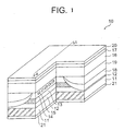
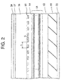
and more particularly to Figures 1 and 2, there is shown a
semiconductor laser device 10 for providing high optical output power,
narrow spectral linewidth, and excellent single-longitudinal mode
lasing characteristics, and which is capable of being manufactured at a
high product yield. Figure 1 is a partially sectional perspective view
showing the structure of a semiconductor laser device according to
the first embodiment of the present invention, and Figure 2 is a
sectional view of the semiconductor laser device taken along the
arrowed line I-I of Figure 1.
The semiconductor device of Figures 1 and 2 is a buried
hetero-junction type DFB laser device including an n-InP substrate 11
having a 1-µm-thick n-InP buffer layer 12, an active layer or active
region 13, and a 200-nm-thick p-InP spacer layer 14 sequentially
stacked on the substrate 11. Buffer layer 12 serves both as a buffer
layer by the n-InP material and a under cladding layer, while the
active layer 13 is a separate confinement multiple quantum well
(SCH-MQW) structure having a 300nm thickness. The MQW active
layers 13 are implemented by a strain-compensated MQW structure
including six QW layers and associated barrier layers. The QW layer
has a compressive strain of 1.0% introduced therein, whereas the
barrier layer has a tensile strain of 0.1% introduced therein for
compensating the compressive strain of the QW layer.
As best seen in Figure 2, a diffraction grating 15 of a GaInAsP
material having a bandgap wavelength λg of about 1450nm and a
refractive index n1 of about 3.46 is periodically formed within the p-InP
spacer layer 14 substantially along the entire length of active layer
13. However, the diffraction grating 15 may be formed over a portion
of the entire length of active layer 13 as shown by the phantom
grating material in Figure 2. The diffraction grating 15 of the
embodiment of Figures 1 and 2 has a film thickness "th" of 20 nm, a
period "A" of 240 nm, and selects a laser beam having a lasing
wavelength λe of 1550 nm to be emitted by the semiconductor laser
device 10. Thus, the lasing wavelength λe is approximately 100 nm
greater than the bandgap wavelength λg of the grating material.
Moreover, the p-InP spacer layer 14 has a refractive index n2 of 3.17,
thereby achieving a difference in the refractive index between the
spacer layer 14 and the diffraction grating 15 (n1 - n2) of
approximately 0.29.
A top portion of the n-InP buffer layer 12, the active layer 13,
and the p-InP spacer layer 14 having the diffraction grating 15 buried
therein form a laminated structure which is etched into mesa stripes so
that the active layer 13 has a width of approximately 1.5 µm. Current
block structures each including a p-InP layer 18 and an n-InP layer 19
are formed on both sides of the mesa stripes. The DFB laser device
10 also has a 2-µm-thick p-InP upper cladding layer 16 and a heavily
doped p-GaInAs contact layer 17 sequentially stacked on the spacer
layer 14 and blocking layers. Also included is a p-side electrode 20
made of a Ti/Pt/Au laminated metal film over the contact layer 17,
and an n-side electrode 21 made of AuGeNi on the bottom surface of
the substrate 11.
While not shown in the figures, the emission facet of the DFB
laser 10 is coated with a non-reflection coat having a reflectance of
about 1%, whereas the rear facet of the DFB laser is coated with a
high-reflection coat having a reflectance of about 90%. Such a
reflectance below about 3% at the emission facet suppresses a Fabry-Perot
mode lasing at the peak wavelength in the optical gain
distribution of the active layer, and in addition, the combination of
this reflectance with a high reflectance above 80% at the rear facet
affords an increase of the output efficiency at the emission facet.
It is to be understood that the device of Figures 1 and 2 is for
exemplary purposes only as many variations of the structure of the
laser device 10 will be readily apparent to one having ordinary skill in
the art. For example, the material composition and layer thicknesses
described may be changed without deviating from the principles of
the present invention. Thus, the embodiment of Figures 1 and 2 are
exemplary for a better understanding of the present invention and the
present invention is not limited to these illustrations.
As noted above, the laser device of the first embodiment
includes a diffraction grating having an emission wavelength λe that
is about 100 nm longer than a bandgap wavelength λg of the grating
material, and the grating material has a refractive index n1 that is
approximately 0.29 higher than a refractive index n2 of the spacer
layer 14. More generally, the first embodiment of the present
invention is designed to meet the following characteristics:
0<λe-λg≤100nm;
and
n1 - n2 > 0.29.
The present inventors have discovered that a DFB laser device
designed with these general characteristics provides the following
improvements over conventional DFB lasers.
First, the DFB laser of the first embodiment has a lower optical
loss for the emission wavelength λe, due to the emission wavelength
λe being longer than the bandgap wavelength λg, thereby achieving a
lower threshold current and an excellent optical output power
characteristic with respect to the injection current. In addition, the
large difference in the refractive index between the diffraction grating
15 and the embedding layer 14 provides a larger coupling coefficient
even with the case of a large distance between the diffraction grating
and the active layer. The larger coupling coefficient has a stable value
due to less sensitivity to the variances in the thickness (height) and the
duty ratio of the diffraction grating, and allows a large number of
DFB lasers to have stable and uniform characteristics, thereby
achieving a higher product yield. The coupling coefficient is
approximately expressed as the following equation:
κ ∝ Γgrating × (n 2 1 - n 2 2) × sin(π w/Λ),
where Γgrating is confinement factor of the mode field into the grating
layer. The present inventors have recognized that when the difference
between n1 and n2 is large, Γgrating can be designed with small value to
obtain a certain κ value. The small Γgrating is realized by increasing the
distance between the diffraction grating and active layer. With small
Γgrating, the factor of Γgrating x sin(π w/Λ) also becomes small, which
indicates the variation of duty ratio makes smaller impact on the
variation of κ.
More specifically, the difference in the refractive index above
0.29 in the DFB lasers suppresses the variance of the coupling
coefficient κ down to ±3cm-1, making it less sensitive to the
variances in the thickness of the diffraction grating, the distance
between the diffraction grating and the active layer and the duty ratio,
which are generally associated with the fabrication process of the
laser device. This allows manufacture of the DFB lasers having a
designed coupling coefficient at a higher product yield. Accordingly,
even for the case of a larger cavity length L, DFB lasers having a
designed normalized coupling coefficient κL can be manufactured
with a stable characteristics, such as having an excellent single-longitudinal-mode
and a narrow spectral linewidth.
In order to further evaluate the DFB laser device 10, the
present inventors tested nine DFB laser types having different cavity
lengths L and coupling coefficients κ. Specifically, the cavity
lengths of the devices were varied among 300, 400 and 500µm, and
the coupling coefficients were varied among 20, 30 and 40cm
-1 for
each of these cavity lengths. These coupling coefficients κ were
obtained by controlling the thickness of the diffraction grating layers
15. Samples of each of the nine sample DFB lasers were subjected to
measurements with respect to the maximum value (SE
max) in the slope
efficiency distribution, the minimum value (SE
min) in the slope
efficiency distribution, the single mode yield (SM
yield (%)), and
another product yield called herein spectral linewidth yield (LW
yield
(%)). Each of the samples tested met the characteristics of 0<λe-λg≤100nm
and n
1 - n
2 > 0.29. In addition, each of the devices tested
had a cavity length L of 300 µm or above to achieve the preferred
power output. The results of these measurements are summarized in
Table 1.
| Sample No | 1 | 2 | 3 | 4 | 5 | 6 | 7 | 8 | 9 |
| κ | cm-1 | 20 | 30 | 40 | 20 | 30 | 40 | 20 | 30 | 40 |
| L | µm | 300 | 300 | 300 | 400 | 400 | 400 | 500 | 500 | 500 |
| κL | | 0.6 | 0.9 | 1.2 | 0.8 | 1.2 | 1.6 | 1.0 | 1.5 | 2.0 |
| SEmax | W/A | 0.49 | 0.47 | 0.45 | 0.45 | 0.42 | 0.4 | 0.4 | 0.37 | 0.35 |
| SEmin | % | 0.33 | 0.3 | 0.28 | 0.32 | 0.29 | 0.26 | 0.2 | 0.17 | 0.14 |
| SMyield | % | 30 | 55 | 68 | 58 | 70 | 77 | 76 | 70 | 70 |
| LWyield | % | 0 | 25 | 43 | 13 | 73 | 90 | 73 | 82 | 100 |
As seen in Table1, this table includes the a parameter κL,
which is the product of the coupling coefficient κ and the length L.
The parameter κL is used to evaluate the recorded data as shown in
Figures 3-6.
Figure 3 shows the SM yield plotted as a function of the κL
values for sample devices manufactured in accordance with the
present invention. The SMyield for each of the sample types was
determined based on the criteria that a sample having a side mode
suppression ratio (SMSR) above 35dB is passed as a non-defective
product, and a device testing 35dB or below is a defective product.
As seen in Figure 3, a κL value above 0.8 abruptly raises the SMyield
compared to a lower κL value below 0.8. Moreover, a κL value
above 1.0 does not afford a significant improvement to SMyield; that is,
the κL above 1.0 does not achieve a SMyield significantly above 70%.
Figure 4 shows LWyield plotted as a function of the κL values
for the sample devices manufactured in accordance with the present
invention. The LWyield for each of the sample types was determined
based on the criteria that a sample having a spectral linewidth below 2
MHz is passed as a non-defective product and a device testing 2MHz
or more is a defective product. As seen in this figure, a κL value in
the range between 0.6 and 2.0 monotonically raises the LWyield.
Moreover, a κL value at about 1.0 in the range abruptly raises the
LWyield up to 70%.
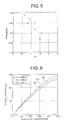
Figure 5 shows SEmax plotted as a function of the κL values
for sample devices manufactured in accordance with the present
invention. As seen in this figure, a lower κL value affords a higher
SEmax, and it is preferable that the κ value be as low as around 20cm-
1 and the cavity length L be smaller for a higher SEmax.
Finally, Fig. 6 shows the optical output power characteristics of
the samples manufactured in accordance with the present invention,
wherein the optical output power (mW) is plotted against the injection
current (mA). As seen in Figure 6, output power was plotted for
devices having each of the κ values tested. Fig. 6 makes clear that a
smaller κ affords a higher slope efficiency to the DFB laser.
Based on the above data, the present inventors determined that
a κL value of greater than 0.8 will achieve a higher SMyield; however,
an excessively higher κL value will reduce the SEmax. In addition, for
a suitable LWyield, the κL value should be 1.0 or above, wherein L
should be larger for a fixed κ value. Accordingly, suitable values for
all of the SEmax, single mode yield SMyield and linewidth yield LWyield
may be achieved by considering the κL value for a DFB laser device.
The selected κL value depends on whether the priority in the design
for the DFB laser resides on the SEmax, single mode yield or linewidth
yield.
For example, if the target design requires an SEmax>0.35 and a
SMyield>50%, then the κL value should satisfy the following
relationship:
0.8< κL<2.0.
It is noted in this case, however, that a κL value below 1.0 involves a
lower linewidth yield. This factor may be taken into account if
linewidth is important to the laser device. As another example, if the
above target design also requires an LWyield>50%, then the κL value
should satisfy the following relationship:
1.0≤κL<2.0.
Alternatively, if a higher efficiency, SEmax>0.4W/A, has a
priority over the single mode yield and the linewidth yield, the κL
value should satisfy the following relationship:
0.8< κL<1.2.
However, as a final example, if the single mode yield and the
linewidth yield have priority over the slope efficiency, then the κL
value should satisfy the following relationship:
1.2≤κL<2.0.
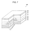
Figure 7 shows a semiconductor laser device 100 for providing
high optical output power, narrow spectral linewidth, and excellent
single-longitudinal mode lasing characteristics, and which is capable
of being manufactured at high product yield, according to another
embodiment of the present invention. As with the first embodiment
shown in Figure 1, the semiconductor device of Figure 7 is a buried
hetero-junction type DFB laser device including an n-InP substrate 22
having a 1-µm-thick n-InP buffer layer 24, an active layer or active
region 26, and a 200-nm-thick p-InP spacer layer 28 sequentially
stacked on the substrate 22. Buffer layer 24 serves both as a buffer
layer by the n-InP material and a under cladding layer, while the
active layer 26 is a separate confinement multiple quantum well
(SCH-MQW) structure having a 300nm thickness.
The MQW active layers 26 are implemented by a strain-compensated
MQW structure including six QW layers and associated
barrier layers. The QW layer has a compressive strain of 1.0%
introduced therein, whereas the barrier layer has a tensile strain of
0.1% introduced therein for compensating the compressive strain of
the QW layer. The strain-compensated MQW structure affords a
higher optical gain to the active layers, thereby reducing the threshold
current and increasing the slope efficiency of the DFB laser. In
addition, the strain-compensated structure improves the long-term
reliability of the laser device. The optimum strains in the QW layers
and the barrier layers depend on the thicknesses of the respective
layers and the number of QW layers in the MQW structure. For
example, where the QW layers have a thickness of 5nm, the barrier
layers have a thickness of 10nm, and the number of QW layers is six,
the preferable compressive strain in the QW layers is around 0.8% to
1.2% whereas the preferable tensile strain in the barrier layers is
around 0.1% to 0.4%.
A diffraction grating 29 of a GaInAsP material having a
bandgap wavelength λg of about 1500nm and a refractive index of
about 3.49 is periodically formed within the p-InP spacer layer 28
substantially along the entire length of active layer 26. In the
embodiment of Figure 7, the active layer has a length, i.e., cavity
length L, of 400µm. The diffraction grating 29 of the embodiment of
Figure 7 has a film thickness "th" of 20 nm, a period "Λ" of 240 nm,
and selects a laser beam having a lasing λe wavelength of 1550 nm to
be emitted by the semiconductor laser device 100. Thus, the lasing
wavelength is approximately 50 nm greater than the bandgap
wavelength λg of the grating material. Moreover, the p-InP spacer
layer 28, embedding therein the diffraction grating 29, has a refractive
index of 3.17, thereby achieving a difference of 0.32 in the refractive
index between the embedding layer 28 and the diffraction grating 29.
Finally, the grating structure of Figure 7 provides a coupling
coefficient κ of 40cm-1, thereby providing a κL parameter of 1.6.
The MQW active layers 26 has a peak wavelength λmax in the
optical gain distribution at 1560nm, thereby achieving a detuning
amount (λe- λmax) at -10nm. The present inventors selected a
detuning amount of -10 nm based on the recognition that the spectral
linewidth in the output laser abruptly increases if the detuning amount
exceeds around +10nm and a detuning amount below +10nm affords
a narrow spectral linewidth. Moreover, the present inventors
recognized that a detuning amount equal to or below -10nm affords an
excellent high-speed modulation. In consideration of the requirements
for a narrow spectral linewidth, for a suitable wavelength distribution
of the optical gain of the active layers and for the stableness in
manufacture of the laser devices, the detuning amount should reside
around -20nm to 0nm. On the other hand, in consideration of the
requirement for the high-speed modulation, the detuning amount
should reside around -20nm to -10nm.
A top portion of the n-InP buffer layer 24, the active layer 26,
and the p-InP spacer layer 28 having the diffraction grating 29 buried
therein form a laminated structure which is etched into mesa stripes so
that the active layer 26 has a width of approximately 1.5 µm. Current
block structures each including a p-InP layer 34 and an n-InP layer 36
are formed on both sides of the mesa stripes. The DFB laser device
100 also has a 2-µm-thick p-InP upper cladding layer 30 and a heavily
doped p-GaInAs contact layer 32 sequentially stacked on the spacer
layer 28 and blocking layers. Also included is a p-side electrode 38
made of a Ti/Pt/Au laminated metal film over the contact layer 32,
and an n-side electrode 40 made of AuGeNi on the bottom surface of
the substrate 22.
The present inventors have confirmed that the DFB laser of the
embodiment of Figure 7 has an optical output power as high as
100mW or more due to the large cavity length selected at 400µm, and
also has a suitable single-longitudinal-mode lasing characteristic
including a spectral linewidth as narrow as 2 MHz or less due to the
specified κL value selected at 1.6. Moreover, the present inventors
discovered that the DFB lasers having these specified characteristics
can be manufactured with a single mode yield as high as 77% and a
linewidth yield as high as 90%. The large difference in the refractive
index between the diffraction grating 29 and the embedding p-InP
spacer layer 28 affords a high coupling coefficient even in the case of
a larger thickness of the p-InP spacer layer 28 which generally
involves a larger distance between the diffraction grating and the
active layers. The large coupling coefficient inevitably results in a
stable coupling coefficient having a smaller variance due to less
sensitivity to variances in the thickness and the duty ratio of the
diffraction grating, whereby DFB lasers having stable characteristics
can be manufactured at a higher product yield due to a larger
tolerance of the process conditions for the epitaxial growth etc.
Obviously, numerous modifications and variations of the
present invention are possible in light of the above teachings. It is
therefore to be understood that within the scope of the appended
claims, the invention may be practiced otherwise than as specifically
described herein.