EP1283282A1 - A method for Cu electroplating in integrated circuit fabrication - Google Patents
A method for Cu electroplating in integrated circuit fabrication Download PDFInfo
- Publication number
- EP1283282A1 EP1283282A1 EP02102036A EP02102036A EP1283282A1 EP 1283282 A1 EP1283282 A1 EP 1283282A1 EP 02102036 A EP02102036 A EP 02102036A EP 02102036 A EP02102036 A EP 02102036A EP 1283282 A1 EP1283282 A1 EP 1283282A1
- Authority
- EP
- European Patent Office
- Prior art keywords
- copper
- layer
- electrolytic solution
- electroplating
- cathode
- Prior art date
- Legal status (The legal status is an assumption and is not a legal conclusion. Google has not performed a legal analysis and makes no representation as to the accuracy of the status listed.)
- Withdrawn
Links
Images

Classifications
-
- H—ELECTRICITY
- H10—SEMICONDUCTOR DEVICES; ELECTRIC SOLID-STATE DEVICES NOT OTHERWISE PROVIDED FOR
- H10W—GENERIC PACKAGES, INTERCONNECTIONS, CONNECTORS OR OTHER CONSTRUCTIONAL DETAILS OF DEVICES COVERED BY CLASS H10
- H10W20/00—Interconnections in chips, wafers or substrates
- H10W20/01—Manufacture or treatment
- H10W20/031—Manufacture or treatment of conductive parts of the interconnections
- H10W20/064—Manufacture or treatment of conductive parts of the interconnections by modifying the conductivity of conductive parts, e.g. by alloying
- H10W20/065—Manufacture or treatment of conductive parts of the interconnections by modifying the conductivity of conductive parts, e.g. by alloying by making at least a portion of the conductive part non-conductive, e.g. by oxidation
-
- C—CHEMISTRY; METALLURGY
- C25—ELECTROLYTIC OR ELECTROPHORETIC PROCESSES; APPARATUS THEREFOR
- C25D—PROCESSES FOR THE ELECTROLYTIC OR ELECTROPHORETIC PRODUCTION OF COATINGS; ELECTROFORMING; APPARATUS THEREFOR
- C25D7/00—Electroplating characterised by the article coated
- C25D7/12—Semiconductors
- C25D7/123—Semiconductors first coated with a seed layer or a conductive layer
-
- H—ELECTRICITY
- H10—SEMICONDUCTOR DEVICES; ELECTRIC SOLID-STATE DEVICES NOT OTHERWISE PROVIDED FOR
- H10P—GENERIC PROCESSES OR APPARATUS FOR THE MANUFACTURE OR TREATMENT OF DEVICES COVERED BY CLASS H10
- H10P14/00—Formation of materials, e.g. in the shape of layers or pillars
- H10P14/40—Formation of materials, e.g. in the shape of layers or pillars of conductive or resistive materials
- H10P14/46—Formation of materials, e.g. in the shape of layers or pillars of conductive or resistive materials using a liquid
- H10P14/47—Electrolytic deposition, i.e. electroplating; Electroless plating
-
- H—ELECTRICITY
- H10—SEMICONDUCTOR DEVICES; ELECTRIC SOLID-STATE DEVICES NOT OTHERWISE PROVIDED FOR
- H10W—GENERIC PACKAGES, INTERCONNECTIONS, CONNECTORS OR OTHER CONSTRUCTIONAL DETAILS OF DEVICES COVERED BY CLASS H10
- H10W20/00—Interconnections in chips, wafers or substrates
- H10W20/01—Manufacture or treatment
- H10W20/031—Manufacture or treatment of conductive parts of the interconnections
- H10W20/064—Manufacture or treatment of conductive parts of the interconnections by modifying the conductivity of conductive parts, e.g. by alloying
Definitions
- the invention is generally related to the field of semiconductor devices and fabrication and more specifically to a method for forming improved copper structures.
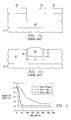
- trenches 40 are first formed in a dielectric layer 20 as shown in Figure 1(a). As illustrated in Figure 1(a) the dielectric layer 20 is formed over a top layer 10 which is formed over a semiconductor substrate containing numerous electronic devices such as transistors, diodes, resistors, etc. In some cases the top layer 10 is a dielectric layer.
- the trench 40 is typically formed using a plasma based etching process and is defined using a patterned photoresist layer 30.
- a liner film 50 is formed in the trench as shown in Figure 1(b).
- copper is used to fill the trench resulting in the copper interconnect structure 60 shown in Figure 1(b).
- the process used to form the copper interconnect structure 60 comprises forming a thick copper layer using a bulk copper fill process followed by chemical mechanical polishing (CMP) to remove the excess copper.
- CMP chemical mechanical polishing
- Copper electroplating has become the most widely used approach for the bulk copper fill process.
- electroplated copper is unstable after plating and will undergo grain growth transformation even at room temperature.
- This grain growth process is beneficial in many ways to the properties of the copper interconnects. Some of these beneficial properties include lower resistivity and better electromigration reliability.
- the grain growth process is very geometry dependent with smaller film geometries underoging a much slower transformation process compared to larger film geometries.
- a comparison of the transformation of blanket copper films is shown in Figure 2 as a function of film thickness.
- the measured resistivity of the copper films is representative of the grain growth taking place in the film. As shown in Figure 2, grain growth in thinner films takes place at a much slower rate than thicker films, indicating a slower rate of grain growth (regrowth).
- Shown in Figure 3 is the percentage reduction in resistance for a 0.75 ⁇ m blanket film 80 and a copper line 90 which is 0.35 ⁇ m wide and 0.8 ⁇ m thick.
- the copper line 90 has a much slower rate of grain growth (regrowth or transformation) compared to the blanket film 80.
- the present invention describes an improved method for electroplating copper in integrated circuit technology.
- the method comprises providing a dielectric layer formed over a semiconductor wafer containing electronic devices such as transistors, capacitors etc. Copper lines are formed in the dielectric layer by first forming a trench in the dielectric layer. A barrier layer of titanium nitride or other suitable material is then formed in the trench. Before the electroplating process is performed a copper seed layer is formed on the barrier layer. With the surface of the copper seed layer acting as the cathode, the copper seed layer is placed in a electrolytic solution containing copper. An electrode is also placed in the electrolytic solution opposite the copper seed layer and a negative potential is applied to the copper seed layer while a positive potention is applied to the electrode. During the electroplating process the electrolytic solution is maintained at a temperature below about 25oC. This results is copper layers with reduced resistivity and improved stability.
- the invention will now be described with reference to Figures 4(a)-4(c) and Figure 5.
- the instant invention is suitable for use in forming copper lines less than 1.0 ⁇ m wide and a few hundred angstroms thick. It will be apparent to those of ordinary skill in the art that the benefits of the invention can be applied to other structures where the electroplating of copper is utilized.
- the electroplating of copper is the leading technology for forming copper lines on integrated circuits. It offers lower cost, faster deposition, and superior copper properties compared to other known methods for copper metallization. These other methods include chemical vapor deposition (CVD), selective electroless deposition, and physical vapor deposition (PVD) or sputtering.
- CVD chemical vapor deposition
- PVD physical vapor deposition
- Electroplating comprises the electrochemical deposition of copper and is caused by the passage of electrical current between two electrodes through a copper sulfate solution, or other copper containing electrolytes.
- a copper sulfate solution or other copper containing electrolytes.
- any number of organic and non-organic additives can be added to improve the electroplating process.
- the electrical current to the electrode is electronic while the current in the electrolyte is ionic.
- electrochemical reduction occurs: Cu 2+ + 2e - -> Cu
- electrochemical oxidation occurs at the anode, usually the reverse reation, if the anode is made of copper.
- copper ions removed at the cathode are replaced by copper ions produced at the anode. Copper ions are transported to the cathode by electric drift, diffusion, and convection.
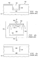
- FIG. 4(a) Shown in Figure 4(a) is a portion of a semiconductor wafer before copper electroplating.
- a dielectric layer 200 is formed over a semiconductor substrate 100.
- the substrate comprises numerous electronic devices such as transistors, diodes, etc.
- a copper line will be formed in the dielectric layer 200 and will form part of the copper interconnect structure of the wafer.
- a trench 350 is etched in the dielectric layer 200 and a barrier layer 300 is formed.
- this barrier layer comprises, tantalum, tantalum nitride (TaN), titanium nitride (TiN), or any suitable material.
- a copper seed layer 400 is formed over the barrier layer 300. This copper seed layer 400 is necessary to provide good electrical contact during the electroplating process as well as good adhesion of the plated copper layer.
- the copper seed layer 400 is typically formed using a CVD or PVD metallization process.
- FIG 4(b) Shown in Figure 4(b) is a simplified diagram of an electrochemical copper plating apparatus.
- the silicon wafer 600 acts as the cathode and a negative potential 800 is applied to the surface of the wafer 450.
- the wafer surface 450 shown in figure 4(a) is exposed to the copper electrolytic solution 500.
- the copper electrolytic solution 500 comprises copper sulfate.
- the anode comprises a copper plate 700 to which a positive voltage is applied. It should be noted that the exact arrangement of the anode, cathode, and copper electrolytic solution will vary.
- Figure 4(b) is therefore intended to illustrate just the basic properties of all electrochemical copper plating systems.
- the surface of the wafer will act as the cathode, the anode will be partially or wholly formed with copper, and both the anode and the cathode will be exposed to a solution comprising copper electrolytes.
- the copper electrolyte solution 500 flows from the anode 700 to the cathode 600 causing a copper layer 650 to form on the surface 450 of the wafer 600.
- the electrolyte solution 500 is usually contained and re-circulated in a vessel 750.
- the wafer 600 is rotated during the electroplating process.
- Shown in Figure 4(c) is the structure of Figure 4(a) after the copper electroplating process.
- the copper layer 650 is shown in Figure 4(c) to have completely filled the trench. Following the formation of the copper layer, chemical mechanical polishing (CMP) is used to remove the excess copper from the surface of the wafer.
- CMP chemical mechanical polishing
- the electrochemical copper process described above is performed at room temperature. This leads to the geometric dependence of the grain growth phenomena described above.
- the geometric dependence of the rate of grain growth (or transformation) can be reduced and/or eliminated.
- Figure 5 shows a series of self annealing curves of copper films electroplated at different temperatures.
- the copper films used to produce the curves shown in Figure 5 where blanket films of equal thickness.
- the sheet resistance of these blanket copper films were measured at room temperature as a function of sit-time or time after formation. As shown in Figure 5 all the films converged to the same sheet resistance value indicating that the initial film thickness were similar.
- Figure 5 clearly shows that as the temperature of the electroplating process is reduced below that of room temperature, the time over which the sheet resistance of the films decrease to their minimum value decreases. This reduction in sheet resistance is indicative of grain growth taking place in the copper films.
- room temperature in the instant invention refers to approximately 25°C. Therefore, by reducing the temperature at which the electroplating process takes place below 25°C, the rate of self annealing grain growth in the copper films increases.
- the temperature of the electroplating process can be controlled below 25°C by ensuring that the solution containing the copper electrolytes, the electrodes (i.e. anode and cathode) and the vessel containing the copper electrolyte solution are all maintained below 25°C, such as at 15°C or 10°C..
- the grain growth in the copper layers can be enhanced by thermal annealing.
- the copper layers formed by electroplating at temperatures below 25°C are thermally annealed by raising the temperature of the copper films above 25°C for a predetermined length of time.
- This thermal annealing can be performed using a conventional furnace or using a rapid thermal processing (RTP) system.
- RTP rapid thermal processing
- the RTP system provides the added advantage of rapidly heating and cooling the copper films thereby reducing the buildup of internal stress in the films.
Landscapes
- Chemical & Material Sciences (AREA)
- Engineering & Computer Science (AREA)
- Chemical Kinetics & Catalysis (AREA)
- Electrochemistry (AREA)
- Materials Engineering (AREA)
- Metallurgy (AREA)
- Organic Chemistry (AREA)
- Internal Circuitry In Semiconductor Integrated Circuit Devices (AREA)
- Electrodes Of Semiconductors (AREA)
- Electroplating Methods And Accessories (AREA)
Abstract
The electroplating of copper is the leading technology for
forming copper lines on integrated circuits. In the copper
electroplating process a negative potential is applied to the
semiconductor wafer with the surface of the semiconductor wafer
acting as the cathode. The anode will be partially or wholly
formed with copper. Both the anode and the semiconductor wafer
will be exposed to a solution comprising copper electrolytes. By
reducing the temperature of the copper electrolyte solution
below 25°C the rate of self annealing grain growth will increase
reducing the final resistively of the copper lines.
Description
- The invention is generally related to the field of semiconductor devices and fabrication and more specifically to a method for forming improved copper structures.
- To increase the operating speed, high performance integrated circuits use copper interconnect technology. Currently the damascene method is the most widely used method for forming copper interconnects. Using this
methodology trenches 40 are first formed in adielectric layer 20 as shown in Figure 1(a). As illustrated in Figure 1(a) thedielectric layer 20 is formed over atop layer 10 which is formed over a semiconductor substrate containing numerous electronic devices such as transistors, diodes, resistors, etc. In some cases thetop layer 10 is a dielectric layer. Thetrench 40 is typically formed using a plasma based etching process and is defined using a patternedphotoresist layer 30. - Following the removal of the photoresist layer 30 a
liner film 50 is formed in the trench as shown in Figure 1(b). Following the formation of theliner film 50, copper is used to fill the trench resulting in thecopper interconnect structure 60 shown in Figure 1(b). The process used to form thecopper interconnect structure 60 comprises forming a thick copper layer using a bulk copper fill process followed by chemical mechanical polishing (CMP) to remove the excess copper. - Copper electroplating has become the most widely used approach for the bulk copper fill process. However, electroplated copper is unstable after plating and will undergo grain growth transformation even at room temperature. This grain growth process is beneficial in many ways to the properties of the copper interconnects. Some of these beneficial properties include lower resistivity and better electromigration reliability. The grain growth process is very geometry dependent with smaller film geometries underoging a much slower transformation process compared to larger film geometries. A comparison of the transformation of blanket copper films is shown in Figure 2 as a function of film thickness. The measured resistivity of the copper films is representative of the grain growth taking place in the film. As shown in Figure 2, grain growth in thinner films takes place at a much slower rate than thicker films, indicating a slower rate of grain growth (regrowth). Shown in Figure 3 is the percentage reduction in resistance for a 0.75 µm blanket film 80 and a copper line 90 which is 0.35µm wide and 0.8µm thick. The copper line 90 has a much slower rate of grain growth (regrowth or transformation) compared to the blanket film 80.
- As integrated circuit technology advances, the width of the copper interconnect structures (70 in Figure 1(b)) and the thickness of these structures (75 in figure 1(b)) will decrease. As this happens the electroplated copper used to form the copper interconnects will be harder to transform. It has been found that if the copper used to form these interconnect structures is not fully transformed, high resistivity and low electromigration resistance will lead to low device yield. There is therefore a need for a method which would result in fully transformed copper in damascene structures for thickness down to 0.1µm and below.
- The present invention describes an improved method for electroplating copper in integrated circuit technology. The method comprises providing a dielectric layer formed over a semiconductor wafer containing electronic devices such as transistors, capacitors etc. Copper lines are formed in the dielectric layer by first forming a trench in the dielectric layer. A barrier layer of titanium nitride or other suitable material is then formed in the trench. Before the electroplating process is performed a copper seed layer is formed on the barrier layer. With the surface of the copper seed layer acting as the cathode, the copper seed layer is placed in a electrolytic solution containing copper. An electrode is also placed in the electrolytic solution opposite the copper seed layer and a negative potential is applied to the copper seed layer while a positive potention is applied to the electrode. During the electroplating process the electrolytic solution is maintained at a temperature below about 25oC. This results is copper layers with reduced resistivity and improved stability.
- In the drawings:
- FIGURES 1(a) - 1(b) are cross-sectional diagrams illustrating the formation of an integrated circuit copper interconnect structure according to the prior art.
- FIGURE 2 shows the variation of copper film resistivity as a function of time after formation for different film thickness'.
- FIGURE 3 shows the resistance reduction percentage of copper lines as a function of time after copper line formation for different copper line widths.
- FIGURES 4(a) - 4(c) are cross-sectional diagrams illustrating a typical copper electroplating process.
- FIGURE 5 shows the sheet resistance of copper films of equal thickness as a function of time after copper film formation.
-
- The invention will now be described with reference to Figures 4(a)-4(c) and Figure 5. The instant invention is suitable for use in forming copper lines less than 1.0µm wide and a few hundred angstroms thick. It will be apparent to those of ordinary skill in the art that the benefits of the invention can be applied to other structures where the electroplating of copper is utilized.
- The electroplating of copper is the leading technology for forming copper lines on integrated circuits. It offers lower cost, faster deposition, and superior copper properties compared to other known methods for copper metallization. These other methods include chemical vapor deposition (CVD), selective electroless deposition, and physical vapor deposition (PVD) or sputtering.
- Electroplating comprises the electrochemical deposition of copper and is caused by the passage of electrical current between two electrodes through a copper sulfate solution, or other copper containing electrolytes. In addition to the copper electrolytes, any number of organic and non-organic additives can be added to improve the electroplating process. The electrical current to the electrode is electronic while the current in the electrolyte is ionic. At the cathode, electrochemical reduction occurs:
- Shown in Figure 4(a) is a portion of a semiconductor wafer before copper electroplating. A
dielectric layer 200 is formed over asemiconductor substrate 100. Here the substrate comprises numerous electronic devices such as transistors, diodes, etc. A copper line will be formed in thedielectric layer 200 and will form part of the copper interconnect structure of the wafer. As shown in Figure 4(a), atrench 350 is etched in thedielectric layer 200 and abarrier layer 300 is formed. In an embodiment of the instant invention this barrier layer comprises, tantalum, tantalum nitride (TaN), titanium nitride (TiN), or any suitable material. Following the formation of thebarrier layer 300, acopper seed layer 400 is formed over thebarrier layer 300. Thiscopper seed layer 400 is necessary to provide good electrical contact during the electroplating process as well as good adhesion of the plated copper layer. Thecopper seed layer 400 is typically formed using a CVD or PVD metallization process. - Shown in Figure 4(b) is a simplified diagram of an electrochemical copper plating apparatus. The
silicon wafer 600 acts as the cathode and anegative potential 800 is applied to the surface of thewafer 450. Thewafer surface 450 shown in figure 4(a) is exposed to the copperelectrolytic solution 500. In an embodiment of the instant invention the copperelectrolytic solution 500 comprises copper sulfate. The anode comprises acopper plate 700 to which a positive voltage is applied. It should be noted that the exact arrangement of the anode, cathode, and copper electrolytic solution will vary. Figure 4(b) is therefore intended to illustrate just the basic properties of all electrochemical copper plating systems. These basic properties are that the surface of the wafer will act as the cathode, the anode will be partially or wholly formed with copper, and both the anode and the cathode will be exposed to a solution comprising copper electrolytes. In the embodiment shown in Figure 4(b), thecopper electrolyte solution 500 flows from theanode 700 to thecathode 600 causing acopper layer 650 to form on thesurface 450 of thewafer 600. Theelectrolyte solution 500 is usually contained and re-circulated in avessel 750. In some applications thewafer 600 is rotated during the electroplating process. Shown in Figure 4(c) is the structure of Figure 4(a) after the copper electroplating process. Thecopper layer 650 is shown in Figure 4(c) to have completely filled the trench. Following the formation of the copper layer, chemical mechanical polishing (CMP) is used to remove the excess copper from the surface of the wafer. - Currently, the electrochemical copper process described above is performed at room temperature. This leads to the geometric dependence of the grain growth phenomena described above. In an embodiment of the instant invention, by performing the electrochemical copper process at temperatures below that of room temperature, the geometric dependence of the rate of grain growth (or transformation) can be reduced and/or eliminated. This is illustrated in Figure 5, which shows a series of self annealing curves of copper films electroplated at different temperatures. The copper films used to produce the curves shown in Figure 5 where blanket films of equal thickness. The sheet resistance of these blanket copper films were measured at room temperature as a function of sit-time or time after formation. As shown in Figure 5 all the films converged to the same sheet resistance value indicating that the initial film thickness were similar. Figure 5 clearly shows that as the temperature of the electroplating process is reduced below that of room temperature, the time over which the sheet resistance of the films decrease to their minimum value decreases. This reduction in sheet resistance is indicative of grain growth taking place in the copper films. It should be noted that room temperature in the instant invention refers to approximately 25°C. Therefore, by reducing the temperature at which the electroplating process takes place below 25°C, the rate of self annealing grain growth in the copper films increases. The temperature of the electroplating process can be controlled below 25°C by ensuring that the solution containing the copper electrolytes, the electrodes (i.e. anode and cathode) and the vessel containing the copper electrolyte solution are all maintained below 25°C, such as at 15°C or 10°C..
- Following the electroplating process the grain growth in the copper layers can be enhanced by thermal annealing. In an embodiment of the instant invention, the copper layers formed by electroplating at temperatures below 25°C are thermally annealed by raising the temperature of the copper films above 25°C for a predetermined length of time. This thermal annealing can be performed using a conventional furnace or using a rapid thermal processing (RTP) system. The RTP system provides the added advantage of rapidly heating and cooling the copper films thereby reducing the buildup of internal stress in the films.
- While this invention has been described with reference to illustrative embodiments, this description is not intended to be construed in a limiting sense. Various modifications and combinations of the illustrative embodiments, as well as other embodiments of the invention will be apparent to persons skilled in the art upon reference to the description. It is therefore intended that the appended claims encompass any such modifications or embodiments.
Claims (10)
- A method for electroplating copper, comprising:providing an electrolytic solution comprising copper;providing an anode in said electrolytic solution;providing a cathode in said electrolytic solution;simultaneously applying a negative potential to said cathode and a positive potential to said anode such that a copper layer is formed on said cathode by copper electroplating; andmaintaining said electrolytic solution at a temperature below room temperature.
- The method of claim 1 wherein said anode comprises copper.
- The method of claim 1 or claim 2 wherein said cathode comprises a silicon wafer.
- The method of claim 1, claim 2 or claim 3 wherein said electrolytic solution comprises copper sulfate.
- The method of any preceding claim further comprising annealing said copper layer at temperatures above room temperature.
- The method of any preceding claim wherein said electrolytic solution is maintained at a temperature below 25°C.
- The method of any preceding claim wherein said electrolytic solution is maintained at a temperature in the range of 10-15°C
- A method for forming copper interconnects, comprising:providing a dielectric layer formed over a semiconductor wafer wherein electronic devices have been formed in said semiconductor wafer;forming a trench in said dielectric layer;forming a barrier layer in said trench;forming a copper seed layer on said barrier layer;placing said copper seed layer in a electrolytic solution containing copper;placing an electrode in said electrolytic solution oppositely positioned from said copper seed layer;simultaneously applying a negative potential to said copper seed layer and a positive voltage to said electrode such that a copper layer is formed on said copper seed layer by electroplating; andmaintaining said electrolytic solution at temperatures below room temperature during said copper layer formation.
- The method of claim 8 further comprising thermally annealing said copper layer at temperatures above room temperature.
- The method of claim 8 or claim 9 further comprising removing a portion of said copper layer using chemical mechanical polishing.
Applications Claiming Priority (2)
| Application Number | Priority Date | Filing Date | Title |
|---|---|---|---|
| US30843401P | 2001-07-27 | 2001-07-27 | |
| US308434 | 2001-07-27 |
Publications (1)
| Publication Number | Publication Date |
|---|---|
| EP1283282A1 true EP1283282A1 (en) | 2003-02-12 |
Family
ID=23193977
Family Applications (1)
| Application Number | Title | Priority Date | Filing Date |
|---|---|---|---|
| EP02102036A Withdrawn EP1283282A1 (en) | 2001-07-27 | 2002-07-18 | A method for Cu electroplating in integrated circuit fabrication |
Country Status (3)
| Country | Link |
|---|---|
| US (1) | US6784104B2 (en) |
| EP (1) | EP1283282A1 (en) |
| JP (1) | JP2003113494A (en) |
Cited By (2)
| Publication number | Priority date | Publication date | Assignee | Title |
|---|---|---|---|---|
| CN102443830A (en) * | 2011-10-12 | 2012-05-09 | 上海华力微电子有限公司 | Method for improving copper electroplating process |
| WO2015076685A1 (en) | 2013-11-22 | 2015-05-28 | Inphotech Sp. O. O. | A method of bonding optical fibers with conductive coatings with metal elements |
Families Citing this family (8)
| Publication number | Priority date | Publication date | Assignee | Title |
|---|---|---|---|---|
| KR100572825B1 (en) * | 2003-07-31 | 2006-04-25 | 동부일렉트로닉스 주식회사 | Metal wiring formation method of semiconductor device |
| US20080128907A1 (en) * | 2006-12-01 | 2008-06-05 | International Business Machines Corporation | Semiconductor structure with liner |
| US9809898B2 (en) * | 2013-06-26 | 2017-11-07 | Lam Research Corporation | Electroplating and post-electrofill systems with integrated process edge imaging and metrology systems |
| US9822460B2 (en) | 2014-01-21 | 2017-11-21 | Lam Research Corporation | Methods and apparatuses for electroplating and seed layer detection |
| US10134670B2 (en) * | 2015-04-08 | 2018-11-20 | International Business Machines Corporation | Wafer with plated wires and method of fabricating same |
| EP3373735A1 (en) * | 2015-11-13 | 2018-09-19 | Basf Se | Substituted oxadiazoles for combating phytopathogenic fungi |
| US9735035B1 (en) | 2016-01-29 | 2017-08-15 | Lam Research Corporation | Methods and apparatuses for estimating on-wafer oxide layer reduction effectiveness via color sensing |
| US12707653B2 (en) * | 2022-09-09 | 2026-08-11 | Taiwan Semiconductor Manufacturing Company, Ltd. | Thick redistribution layer features |
Citations (4)
| Publication number | Priority date | Publication date | Assignee | Title |
|---|---|---|---|---|
| EP0952242A1 (en) * | 1998-04-21 | 1999-10-27 | Applied Materials, Inc. | Electro deposition chemistry |
| US6103624A (en) * | 1999-04-15 | 2000-08-15 | Advanced Micro Devices, Inc. | Method of improving Cu damascene interconnect reliability by laser anneal before barrier polish |
| US6103086A (en) * | 1999-01-05 | 2000-08-15 | Advanced Micro Devices, Inc. | Method of forming reliable copper interconnects with improved hole filling |
| EP1152071A1 (en) * | 1999-01-28 | 2001-11-07 | Electroplating Engineers of Japan Limited | Copper plating method |
Family Cites Families (4)
| Publication number | Priority date | Publication date | Assignee | Title |
|---|---|---|---|---|
| JPH0452296A (en) * | 1990-06-20 | 1992-02-20 | Permelec Electrode Ltd | Copper plating method |
| US5830374A (en) * | 1996-09-05 | 1998-11-03 | International Business Machines Corporation | Method for producing multi-layer circuit board and resulting article of manufacture |
| US5933758A (en) * | 1997-05-12 | 1999-08-03 | Motorola, Inc. | Method for preventing electroplating of copper on an exposed surface at the edge exclusion of a semiconductor wafer |
| US6024856A (en) * | 1997-10-10 | 2000-02-15 | Enthone-Omi, Inc. | Copper metallization of silicon wafers using insoluble anodes |
-
2002
- 2002-07-12 US US10/194,592 patent/US6784104B2/en not_active Expired - Lifetime
- 2002-07-18 EP EP02102036A patent/EP1283282A1/en not_active Withdrawn
- 2002-07-24 JP JP2002215033A patent/JP2003113494A/en active Pending
Patent Citations (4)
| Publication number | Priority date | Publication date | Assignee | Title |
|---|---|---|---|---|
| EP0952242A1 (en) * | 1998-04-21 | 1999-10-27 | Applied Materials, Inc. | Electro deposition chemistry |
| US6103086A (en) * | 1999-01-05 | 2000-08-15 | Advanced Micro Devices, Inc. | Method of forming reliable copper interconnects with improved hole filling |
| EP1152071A1 (en) * | 1999-01-28 | 2001-11-07 | Electroplating Engineers of Japan Limited | Copper plating method |
| US6103624A (en) * | 1999-04-15 | 2000-08-15 | Advanced Micro Devices, Inc. | Method of improving Cu damascene interconnect reliability by laser anneal before barrier polish |
Cited By (2)
| Publication number | Priority date | Publication date | Assignee | Title |
|---|---|---|---|---|
| CN102443830A (en) * | 2011-10-12 | 2012-05-09 | 上海华力微电子有限公司 | Method for improving copper electroplating process |
| WO2015076685A1 (en) | 2013-11-22 | 2015-05-28 | Inphotech Sp. O. O. | A method of bonding optical fibers with conductive coatings with metal elements |
Also Published As
| Publication number | Publication date |
|---|---|
| JP2003113494A (en) | 2003-04-18 |
| US6784104B2 (en) | 2004-08-31 |
| US20030022493A1 (en) | 2003-01-30 |
Similar Documents
| Publication | Publication Date | Title |
|---|---|---|
| US7129165B2 (en) | Method and structure to improve reliability of copper interconnects | |
| US6429523B1 (en) | Method for forming interconnects on semiconductor substrates and structures formed | |
| EP0982771B1 (en) | Process for semiconductor device fabrication having copper interconnects | |
| CN100481377C (en) | Semiconductor device and method for manufacturing the same | |
| CN100399524C (en) | Electroplated CoWP composite structure as copper barrier layer | |
| US20010011638A1 (en) | Method of forming a metal seed layer for subsequent plating | |
| JP2001185510A (en) | Barrier layer for electroplating | |
| US6380083B1 (en) | Process for semiconductor device fabrication having copper interconnects | |
| CN100517684C (en) | Semiconductor device and method for manufacturing same | |
| US8785321B2 (en) | Low resistance and reliable copper interconnects by variable doping | |
| US20060091551A1 (en) | Differentially metal doped copper damascenes | |
| US7659198B2 (en) | In-situ deposition for Cu hillock suppression | |
| US6784104B2 (en) | Method for improved cu electroplating in integrated circuit fabrication | |
| US6861354B2 (en) | Method and structure to reduce defects in integrated circuits and substrates | |
| US7268075B2 (en) | Method to reduce the copper line roughness for increased electrical conductivity of narrow interconnects (<100nm) | |
| US20140103534A1 (en) | Electrochemical deposition on a workpiece having high sheet resistance | |
| WO2002101817A2 (en) | Method and apparatus for controlling a thickness of a copper film | |
| US6955984B2 (en) | Surface treatment of metal interconnect lines | |
| US20040009659A1 (en) | Method of forming copper wiring in a semiconductor device | |
| KR100701673B1 (en) | Copper wiring formation method of semiconductor device | |
| KR100896159B1 (en) | Semiconductor device and method for manufacturing same | |
| JP3441374B2 (en) | Film formation method | |
| KR100451767B1 (en) | Method for forming interconnect structures of semiconductor device | |
| US20040259376A1 (en) | Method of reducing stress migration in integrated circuits | |
| JPH06120212A (en) | Method for manufacturing semiconductor device |
Legal Events
| Date | Code | Title | Description |
|---|---|---|---|
| PUAI | Public reference made under article 153(3) epc to a published international application that has entered the european phase |
Free format text: ORIGINAL CODE: 0009012 |
|
| AK | Designated contracting states |
Designated state(s): AT BE BG CH CY CZ DE DK EE ES FI FR GB GR IE IT LI LU MC NL PT SE SK TR |
|
| AX | Request for extension of the european patent |
Extension state: AL LT LV MK RO SI |
|
| 17P | Request for examination filed |
Effective date: 20030731 |
|
| AKX | Designation fees paid |
Designated state(s): DE FR GB |
|
| RBV | Designated contracting states (corrected) |
Designated state(s): DE FR GB |
|
| 17Q | First examination report despatched |
Effective date: 20071127 |
|
| STAA | Information on the status of an ep patent application or granted ep patent |
Free format text: STATUS: THE APPLICATION IS DEEMED TO BE WITHDRAWN |
|
| 18D | Application deemed to be withdrawn |
Effective date: 20080508 |