EP1282229A1 - Digitally controlled analog delay locked loop (DLL) - Google Patents
Digitally controlled analog delay locked loop (DLL) Download PDFInfo
- Publication number
- EP1282229A1 EP1282229A1 EP01127404A EP01127404A EP1282229A1 EP 1282229 A1 EP1282229 A1 EP 1282229A1 EP 01127404 A EP01127404 A EP 01127404A EP 01127404 A EP01127404 A EP 01127404A EP 1282229 A1 EP1282229 A1 EP 1282229A1
- Authority
- EP
- European Patent Office
- Prior art keywords
- signal
- delay
- response
- circuit
- control
- Prior art date
- Legal status (The legal status is an assumption and is not a legal conclusion. Google has not performed a legal analysis and makes no representation as to the accuracy of the status listed.)
- Granted
Links
- 230000004044 response Effects 0.000 claims abstract description 49
- 238000000034 method Methods 0.000 claims description 10
- 230000001419 dependent effect Effects 0.000 claims 2
- 238000010586 diagram Methods 0.000 description 34
- 239000003990 capacitor Substances 0.000 description 9
- 230000000630 rising effect Effects 0.000 description 9
- 230000000295 complement effect Effects 0.000 description 8
- 230000007704 transition Effects 0.000 description 8
- 239000000872 buffer Substances 0.000 description 4
- 239000002184 metal Substances 0.000 description 3
- 230000008859 change Effects 0.000 description 2
- 230000003247 decreasing effect Effects 0.000 description 2
- 230000001934 delay Effects 0.000 description 2
- 101100191136 Arabidopsis thaliana PCMP-A2 gene Proteins 0.000 description 1
- 101100048260 Saccharomyces cerevisiae (strain ATCC 204508 / S288c) UBX2 gene Proteins 0.000 description 1
- 238000007796 conventional method Methods 0.000 description 1
- 230000008878 coupling Effects 0.000 description 1
- 238000010168 coupling process Methods 0.000 description 1
- 238000005859 coupling reaction Methods 0.000 description 1
- 230000003111 delayed effect Effects 0.000 description 1
- 230000009977 dual effect Effects 0.000 description 1
- 238000005516 engineering process Methods 0.000 description 1
- 230000006870 function Effects 0.000 description 1
- 230000003071 parasitic effect Effects 0.000 description 1
- 230000008569 process Effects 0.000 description 1
- 230000001902 propagating effect Effects 0.000 description 1
- 239000000758 substrate Substances 0.000 description 1
- 230000001960 triggered effect Effects 0.000 description 1
Images


Classifications
-
- H—ELECTRICITY
- H03—ELECTRONIC CIRCUITRY
- H03L—AUTOMATIC CONTROL, STARTING, SYNCHRONISATION OR STABILISATION OF GENERATORS OF ELECTRONIC OSCILLATIONS OR PULSES
- H03L7/00—Automatic control of frequency or phase; Synchronisation
- H03L7/06—Automatic control of frequency or phase; Synchronisation using a reference signal applied to a frequency- or phase-locked loop
- H03L7/08—Details of the phase-locked loop
-
- H—ELECTRICITY
- H03—ELECTRONIC CIRCUITRY
- H03K—PULSE TECHNIQUE
- H03K5/00—Manipulating of pulses not covered by one of the other main groups of this subclass
- H03K5/13—Arrangements having a single output and transforming input signals into pulses delivered at desired time intervals
- H03K5/133—Arrangements having a single output and transforming input signals into pulses delivered at desired time intervals using a chain of active delay devices
-
- H—ELECTRICITY
- H03—ELECTRONIC CIRCUITRY
- H03L—AUTOMATIC CONTROL, STARTING, SYNCHRONISATION OR STABILISATION OF GENERATORS OF ELECTRONIC OSCILLATIONS OR PULSES
- H03L7/00—Automatic control of frequency or phase; Synchronisation
- H03L7/06—Automatic control of frequency or phase; Synchronisation using a reference signal applied to a frequency- or phase-locked loop
- H03L7/08—Details of the phase-locked loop
- H03L7/081—Details of the phase-locked loop provided with an additional controlled phase shifter
- H03L7/0812—Details of the phase-locked loop provided with an additional controlled phase shifter and where no voltage or current controlled oscillator is used
- H03L7/0814—Details of the phase-locked loop provided with an additional controlled phase shifter and where no voltage or current controlled oscillator is used the phase shifting device being digitally controlled
-
- H—ELECTRICITY
- H03—ELECTRONIC CIRCUITRY
- H03L—AUTOMATIC CONTROL, STARTING, SYNCHRONISATION OR STABILISATION OF GENERATORS OF ELECTRONIC OSCILLATIONS OR PULSES
- H03L7/00—Automatic control of frequency or phase; Synchronisation
- H03L7/06—Automatic control of frequency or phase; Synchronisation using a reference signal applied to a frequency- or phase-locked loop
- H03L7/08—Details of the phase-locked loop
- H03L7/081—Details of the phase-locked loop provided with an additional controlled phase shifter
- H03L7/0812—Details of the phase-locked loop provided with an additional controlled phase shifter and where no voltage or current controlled oscillator is used
- H03L7/0816—Details of the phase-locked loop provided with an additional controlled phase shifter and where no voltage or current controlled oscillator is used the controlled phase shifter and the frequency- or phase-detection arrangement being connected to a common input
-
- H—ELECTRICITY
- H03—ELECTRONIC CIRCUITRY
- H03L—AUTOMATIC CONTROL, STARTING, SYNCHRONISATION OR STABILISATION OF GENERATORS OF ELECTRONIC OSCILLATIONS OR PULSES
- H03L7/00—Automatic control of frequency or phase; Synchronisation
- H03L7/06—Automatic control of frequency or phase; Synchronisation using a reference signal applied to a frequency- or phase-locked loop
- H03L7/08—Details of the phase-locked loop
- H03L7/081—Details of the phase-locked loop provided with an additional controlled phase shifter
- H03L7/0812—Details of the phase-locked loop provided with an additional controlled phase shifter and where no voltage or current controlled oscillator is used
- H03L7/0818—Details of the phase-locked loop provided with an additional controlled phase shifter and where no voltage or current controlled oscillator is used the controlled phase shifter comprising coarse and fine delay or phase-shifting means
-
- H—ELECTRICITY
- H03—ELECTRONIC CIRCUITRY
- H03L—AUTOMATIC CONTROL, STARTING, SYNCHRONISATION OR STABILISATION OF GENERATORS OF ELECTRONIC OSCILLATIONS OR PULSES
- H03L7/00—Automatic control of frequency or phase; Synchronisation
- H03L7/06—Automatic control of frequency or phase; Synchronisation using a reference signal applied to a frequency- or phase-locked loop
- H03L7/08—Details of the phase-locked loop
- H03L7/085—Details of the phase-locked loop concerning mainly the frequency- or phase-detection arrangement including the filtering or amplification of its output signal
- H03L7/087—Details of the phase-locked loop concerning mainly the frequency- or phase-detection arrangement including the filtering or amplification of its output signal using at least two phase detectors or a frequency and phase detector in the loop
-
- H—ELECTRICITY
- H03—ELECTRONIC CIRCUITRY
- H03K—PULSE TECHNIQUE
- H03K5/00—Manipulating of pulses not covered by one of the other main groups of this subclass
- H03K2005/00013—Delay, i.e. output pulse is delayed after input pulse and pulse length of output pulse is dependent on pulse length of input pulse
- H03K2005/00019—Variable delay
- H03K2005/00026—Variable delay controlled by an analog electrical signal, e.g. obtained after conversion by a D/A converter
-
- H—ELECTRICITY
- H03—ELECTRONIC CIRCUITRY
- H03K—PULSE TECHNIQUE
- H03K5/00—Manipulating of pulses not covered by one of the other main groups of this subclass
- H03K2005/00013—Delay, i.e. output pulse is delayed after input pulse and pulse length of output pulse is dependent on pulse length of input pulse
- H03K2005/0015—Layout of the delay element
- H03K2005/00195—Layout of the delay element using FET's
- H03K2005/00208—Layout of the delay element using FET's using differential stages
-
- H—ELECTRICITY
- H03—ELECTRONIC CIRCUITRY
- H03K—PULSE TECHNIQUE
- H03K5/00—Manipulating of pulses not covered by one of the other main groups of this subclass
- H03K2005/00013—Delay, i.e. output pulse is delayed after input pulse and pulse length of output pulse is dependent on pulse length of input pulse
- H03K2005/0015—Layout of the delay element
- H03K2005/00234—Layout of the delay element using circuits having two logic levels
- H03K2005/00241—Layout of the delay element using circuits having two logic levels using shift registers
Definitions
- the bandwidth of the DLL 10 can be reduced.
- the bandwidth is reduced when the capacitance of the loop filter 20 is made large and/or the current from the charge pump 18 is made small.
- every up/down cycle of the phase detector only adjusts the phase of the signal DLL_CLOCK by a small amount or not at all when the reference clock REF_CLOCK and the feedback signal FBK have zero degrees of phase error.
- the bandwidth of the DLL can be made wider by decreasing the capacitor size and/or increasing the charge pump current.
- every up/down cycle of the phase detector adjusts the phase of the signal DLL_CLOCK by a greater amount than for the fine adjustment (small bandwidths).
- the analog DLL 10 can provide good resolution. However, using lock acquisition aids that change the charge pump currents or the loop filter can make designing for stability complicated. Also, the analog DLL 10 is limited as to how fast lock can be obtained. In addition, different locking methods can be difficult to implement; such as a binary search.
- the circuit 100 may be implemented as a digitally controlled analog delay locked loop (DLL).
- the circuit 100 may have an input 102 that may receive a reference clock (e.g., REF_CLK) and an output 104 that may present a signal (e.g., CLK_OUT).
- the circuit 100 may be configured to generate the signal CLK_OUT having an edge (e.g., rising or falling) that precedes a corresponding edge of the signal REF_CLK by a predetermined period of time (e.g., tco).
- the signal CLK_OUT may track the jitter and duty cycle of the signal REF_CLK.
- a complement of the signal REF_CLK (e.g., REF_CLKB) may be presented to a first input of the gates 190 and 194.
- An output of the gate 190 may be presented to an input of the storage element 192.
- a complement of the signal FBK (e.g., FBKB) may be presented to a clock input of the storage elements 192 and 196.
- the storage element 192 may have an output (e.g., QB) that may be connected to a second input of the gate 190 and the output (e.g., Q) that may present the signal CNT to a second input of a gate 194.
- An output of the gate 194 may present a signal to an input of the storage element 196.
- the storage element 196 may be configured to present the signal SFTR at a QB-output.
- the circuits 224a-224n may have a first input that may receive the signal VPBIAS, the second input that may receive the signal WBIAS, a third input that may receive the signal VCTRL, a fourth input that may receive the signal REF_CLK and a fifth input that may receive a complement of the signal REF_CLK (e.g., REF_CLKB).
- Each of the circuits 224a-224n may have an output that may be connected together to form a node 228.
- the signal CLK_OUT may be presented at the node 228.
- a source of each of the transistors 244-250 may be coupled to a supply ground (e.g., VSS) via a transistor 252.
- a signal (e.g., PREV) may be presented to a gate of the transistor 252.
- the signal PREV may be used to switch the delay cell 232 ON and OFF.
- the signal PREV may be implemented to disable the delay cells 232 to reduce dc current dissipation.
- each delay cell 232 may start with three delay elements 224 (6 delay cells 232) enabled.
- the number of enabled delay elements 224 generally sets the minimum delay in the delay chain 170.
- each delay cell 232 may have, in one example, a delay range of 200ps to 333ps (0.2+2*0.4ns/6).
- the circuit 100 may use the actual clock to output delay (tco) except for the FIFO, driver, and package parasitics/loads to adjust the phase of the signals CLK_OUT and CLK_OUTB.
- the "dummy" driver may be a cut-down version of the real driver but generally also uses VCCQ/VSSQ to match the delay due to the power supplies.
- a timing diagram 320 is shown illustrating an example operation of the present invention.
- the timing diagram may illustrate an example operation when the clock cycle delay around the loop is greater than two cycles.
- the signal UP2 generally transitions to a logical HIGH state.
- the circuit 100 may have a disabled mode. When the circuit 100 is disabled, the delay locked loop (DLL) is generally bypassed. When the DLL is bypassed, the DLL may be multiplexed out. The DLL may be in a reset mode as well. When the circuit 100 is re-enabled, the DLL is generally initialized to a redetermined starting point to assure proper operation.
- DLL delay locked loop
Landscapes
- Physics & Mathematics (AREA)
- Nonlinear Science (AREA)
- Pulse Circuits (AREA)
- Stabilization Of Oscillater, Synchronisation, Frequency Synthesizers (AREA)
- Dram (AREA)
Abstract
Description
- The present invention relates to a method and/or architecture for Delay Locked Loops (DLLs) generally and, more particularly, to a method and/or architecture for a digitally controlled analog Delay Locked Loop (DLL).
- Some applications can require that data be valid less than 0.35ns (250MHz) from a rising clock edge. The clock to data valid (tco) time and the data output hold time (tdoh) dictate the data valid window. Also, the duty cycle of the data can be required to follow the duty cycle of the clock so that the data valid window is not reduced. A zero delay buffer that tracks the clock jitter and duty cycle can be used to meet the requirements.
- A conventional zero delay buffer that tracks the clock jitter and duty cycle can include a Delay Locked Loop (DLL). The DLL can generate a phase-adjusted version of an input clock such that a desired edge (e.g., rising or falling) of the DLL clock occurs a time tco before a corresponding edge of the input clock. The phase-adjusted clock can be used to clock data out of a chip so that the data to input clock time is ideally zero.
- The DLL is a closed loop system that adjusts the propagation through a delay line such that the delay is equal to the clock period minus the clock to output delay. A phase detector and filter adjust the delay line until a feedback clock is delayed 360 degrees (i.e., phase aligned) with respect to the input clock. Since the compensation delay can be set equal to the time tco, the delay line can have a delay equal to the clock period minus the time tco.
- Every cycle the DLL makes an adjustment with the phase detector and filter that corresponds to a phase adjustment in the delay line. The adjustment determines the resolution of the DLL. A fine adjustment corresponds to a small phase adjustment (high resolution) and a coarse adjustment corresponds to a large phase adjustment (low resolution). The DLL needs to have a fast lock time and a fine resolution for low jitter. A fast lock time requires a coarse adjustment in the delay line and a fine resolution requires a fine adjustment in the delay line.
- Conventional DLLs either use a digital delay line or an analog delay line. A digital delay line can provide fast lock time at the cost of resolution. An analog delay line can provide good resolution but can require lock acquisition aids such as changing charge pump currents that can cause problems.
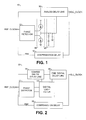
- Referring to FIG. 1, a block diagram of a
circuit 10 is shown illustrating an analog DLL. Thecircuit 10 includes aphase detector 12, ananalog delay line 14, acompensation delay circuit 16, acharge pump 18 and ananalog loop filter 20. Thephase detector 12 is implemented without a dead zone. Theanalog delay line 14 can provide minimal jitter. Thecircuit 10 integrates phase error onto a capacitor in thefilter 20. Since the phase error is integrated onto a capacitor and the phase detector does not have a dead zone, thecircuit 10 can provide low clock jitter or fine resolution. - To reduce jitter of the signal DLL_CLOCK, the bandwidth of the
DLL 10 can be reduced. The bandwidth is reduced when the capacitance of theloop filter 20 is made large and/or the current from thecharge pump 18 is made small. With reduced bandwidth, every up/down cycle of the phase detector only adjusts the phase of the signal DLL_CLOCK by a small amount or not at all when the reference clock REF_CLOCK and the feedback signal FBK have zero degrees of phase error. For coarse adjustment, the bandwidth of the DLL can be made wider by decreasing the capacitor size and/or increasing the charge pump current. For large bandwidths, every up/down cycle of the phase detector adjusts the phase of the signal DLL_CLOCK by a greater amount than for the fine adjustment (small bandwidths). - The
analog DLL 10 can provide good resolution. However, using lock acquisition aids that change the charge pump currents or the loop filter can make designing for stability complicated. Also, theanalog DLL 10 is limited as to how fast lock can be obtained. In addition, different locking methods can be difficult to implement; such as a binary search. - Referring to FIG. 2, a block diagram of a
circuit 30 is shown illustrating a digital DLL. Thecircuit 30 includes aphase detector 32, a coarsedigital delay line 34, a finedigital delay line 36, a compensation delay 28 and adigital loop filter 40. Thedigital DLL 30 can yield a smaller (size), faster locking, and easier migrating DLL. Thedigital DLL 30 uses thecoarse delay line 34 to get close to lock and thefine delay line 36 to obtain and maintain lock. The charge pump and filter (i.e.,elements digital loop filter 40. Thedigital loop filter 40 includes an up/down counter that only increments/decrements every M up/down cycles, where M is determined by the filter size. - The
digital DLL 30 can be less complicated and has a faster lock time than theanalog DLL 10. Thedigital DLL 30 can be easier to migrate to other technologies. Thedigital DLL 30 can be smaller than theanalog DLL 10 because there is no large loop filter. However, since the fine delay line is a digital element, the resolution is limited to some amount. Also, since the phase error is not integrated, the output can have a dead zone where thedigital DLL 30 does not respond until a phase error reaches a particular magnitude. When the particular magnitude of phase error occurs, theDLL 30 is adjusted by the fine adjust. - The present invention concerns an apparatus comprising an analog delay line and a control circuit. The analog delay line may be configured to generate an output signal in response to an input signal, a first control signal, and a second control signal. A phase of the output signal may be (i) coarsely adjustable with respect to the input signal in response to the first control signal and (ii) finely and continuously adjustable in response to the second control signal. The control circuit may be configured to generate the first and the second control signals in response to the input signal and the output signal.
- The objects, features and advantages of the present invention include providing a digitally controlled analog delay locked loop that may (i) provide fine resolution, (ii) have fast lock acquisition, (iii) provide a wide locking range, (iv) eliminate need for fuses or metal optioning for different speed sorts, (v) provide lower speed sorts that have the same resolution as higher speed sorts, and/or (vi) be used in applications that need a zero delay buffer including memory chips that need a small clock to output delay.
- These and other objects, features and advantages of the present invention will be apparent from the following detailed description and the appended claims and drawings in which:
- FIG. 1 is a block diagram of an analog delay lock loop circuit;
- FIG. 2 is a block diagram of a digital delay lock loop circuit;
- FIG. 3 is a top level diagram of a preferred embodiment of the present invention;
- FIG. 4 is a block diagram of a preferred embodiment of the present invention;
- FIG. 5 is a detailed block diagram of a fine phase detector of FIG. 4;
- FIG. 6 is a detailed block diagram of a course phase detector of FIG. 4;
- FIG. 7 is a detailed block diagram of a control logic of FIG. 4;
- FIG. 8 is a detailed block diagram of an analog delay line of FIG. 4;
- FIG. 9 is a detailed block diagram of a delay element of FIG. 8;
- FIG. 10 is a block diagram of a register element of FIG. 8;
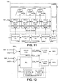
- FIG. 11 is a block diagram illustrating an example operation path of the present invention;
- FIG. 12 is a block diagram illustrating an alternative embodiment of the present invention;
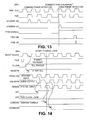
- FIG. 13 is a timing diagram illustrating an example operation of the present invention;
- FIG. 14 is a timing diagram illustrating an example reset operation of the present invention;
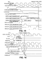
- FIG. 15 is a timing diagram illustrating an example coarse adjustment operation of the present invention; and
- FIG. 16 is a timing diagram illustrating a dual clock adjustment in accordance with the present invention.
-
- Referring to FIG. 3, a top level diagram of a
circuit 100 is shown in accordance with a preferred embodiment of the present invention. Thecircuit 100 may be implemented as a digitally controlled analog delay locked loop (DLL). Thecircuit 100 may have an input 102 that may receive a reference clock (e.g., REF_CLK) and anoutput 104 that may present a signal (e.g., CLK_OUT). Thecircuit 100 may be configured to generate the signal CLK_OUT having an edge (e.g., rising or falling) that precedes a corresponding edge of the signal REF_CLK by a predetermined period of time (e.g., tco). The signal CLK_OUT may track the jitter and duty cycle of the signal REF_CLK. - The
circuit 100 may comprise acircuit 110, acircuit 112, acircuit 114, acircuit 116, acircuit 118, acircuit 120 and acircuit 122. Thecircuit 110 may be implemented as a fine (resolution) phase detector circuit. Thecircuit 112 may be implemented as a coarse (resolution) phase detector circuit. Thecircuit 114 may be implemented as an analog delay line. Thecircuit 114 may be configured to provide a delay that may be both coarsely and finely adjusted. Thecircuit 116 may be implemented as a compensation delay circuit. In one example, thecircuit 116 may be implemented to compensate for a clock to output delay time (tco) of a memory circuit. Thecircuit 118 may be implemented as a control circuit. In one example, thecircuit 118 may be implemented using digital logic. Thecircuit 120 may be implemented as a charge pump circuit. Thecircuit 122 may be implemented as an analog filter circuit. - The signal REF_CLK may be presented to an
input 124 of thecircuit 110, aninput 126 of thecircuit 112 and aninput 128 of thecircuit 114. Thecircuit 110 may have aninput 130 that may receive a signal (e.g., FBK), anoutput 132 that may present a control signal (e.g., UPF) that may be presented to a first input of thecircuit 120, and anoutput 134 that may present a second control signal (e.g., DNF) that may be presented to a second input of thecircuit 120. The signal FBK may be a feedback signal generated in response to the signal CLK_OUT. The signals UPF and DNF may be charge pump control signals (e.g., pump-up and pump-down, respectively). In one example, the signals UPF and DNF may be used to make fine phase adjustments in the signal CLK_OUT. - The signal FBK may be presented to an
input 136 of thecircuit 112. Thecircuit 112 may be configured to generate a number of control signals that may be used to control thecircuit 118. In one example, thecircuit 112 may have anoutput 138 that may present a control signal (e.g., UPC) to aninput 140 of thecircuit 118 and anoutput 142 that may present a control signal (e.g., DNC) to aninput 144 of thecircuit 118. The signals UPC and DNC may be used to make coarse phase adjustments. For example, the signal UPC may be used to increase a range of delay provided by thecircuit 100. The signal DNC may be used to decrease the range of delay provided by thecircuit 100. Further description of the signals UPC and DNC may be found below in connection with FIG. 13. Alternatively, other types and numbers of control signals may be generated by thecircuit 112 to meet the design criteria of a particular implementation. - The
circuit 114 may have aninput 146 that may receive a signal (e.g., VCTRL), aninput 148 that may receive a signal (e.g., DLY_RANGE), and anoutput 150 that may present the signal CLK_OUT. Thecircuit 114 may be configured to select a range of delays in response to the signal DLY_RANGE. Thecircuit 114 may be further configured to generate a delay that may be finely and continuously varied within the particular range selected in response to the signal VCTRL. Thecircuit 114 may be configured to generate the signal CLK_OUT as a phase-adjusted version of the signal REF_CLK, where the phase adjustment is determined in response to the signals VCTRL and DLY_RANGE. - The
circuit 116 may have aninput 152 that may receive the signal CLK_OUT and an output 154 that may present the signal FBK. Thecircuit 116 may be configured to generate the signal FBK in response to the signal CLK_OUT. In one example, thecircuit 116 may be configured to compensate for a clock to output delay (tco) of a memory device. However, other delays may be compensated accordingly to meet the design criteria of a particular application. - The
circuit 118 may have anoutput 156 that may present the signal DLY_RANGE and aninput 158 that may receive the signal CLK_OUT. The signal DLY_RANGE may comprise one or more signals. In one example, the signal DLY_RANGE may be a multi-bit signal where each of the bits may be used as an independent control signal. The signal DLY_RANGE may be presented, in one example, as either a parallel or a serial (multiplexed) signal. Alternatively, the signal DLY_RANGE may comprise a clock signal and one or more control signals. In one example, thecircuit 118 may be configured to generate the signal DLY_RANGE in response to the signals UPC, DNC and CLK_OUT. Alternatively, thecircuit 118 may be configured to use either the signal REF_CLK or the signal FBK in place of CLK_OUT. - The
circuit 120 may have an output that may present a signal to an input of thecircuit 122. Thecircuit 120 may be configured to generate, in one example, a current signal in response to the signals UPF and DNF. Thecircuit 120 may comprise a number of current sources that may be controlled using the signals UPF and DNF. - The
circuit 122 may comprise a number of filter elements. In one example, thecircuit 122 may comprise a resistor, a first capacitor, and a second capacitor. A node 159 may be formed by connecting the input and output of thecircuit 122 to a first terminal of the resistor and a first terminal of the first capacitor. A second terminal of the resistor may be connected to a first terminal of the second capacitor. A second terminal of the first capacitor and the second capacitor may be connected to a supply ground. The signal VCTRL may be presented at the node 159. The signal VCTRL may be generated in response to the signals UPF and DNF. - Referring to FIG. 4, a more detailed block diagram of the
circuit 100 is shown. Thecircuit 110 may have an enableinput 160 that may receive a signal (e.g., EN) from anoutput 162 of thecontrol circuit 118. A signal (e.g., CNT) and a signal (e.g., SFTR) may be presented at theoutputs circuit 112, respectively. The signal CNT may be implemented, in one example, as a count signal. The signal SFTR may be implemented as a shift control signal. - The
circuit 114 may have an input 164 that may receive a control signal (e.g., BYPASS) and aninput 166 that may receive a control signal (e.g., RESET). The signal BYPASS may be used to bypass thedelay line 114. When the signal BYPASS is in an asserted state, the signal REF_CLK may be passed without delay to theoutput 150. The signal RESET may be a control signal. Thedelay line 114 may be configured to enter a preconditioned or initialized state in response to the signal RESET. For example, thecircuit 114 may be configured to (i) set a number of registers (e.g., 3) to a logical HIGH state, or "one" and (ii) reset any remaining registers to a logical LOW, or "zero", in response to the signal RESET. When thecircuit 114 is initialized (reset), a predetermined minimum amount of delay is generally selected (as discussed in more detail in connection with FIG. 11). - The
circuit 114 may comprise acircuit 170 and acircuit 172. Thecircuit 170 may be implemented as a delay chain. Thecircuit 172 may be implemented as a shift register. Thecircuit 170 may receive the signal REF_CLK, the signal VCTRL, and one or more control signals (e.g., SEL0-SELn) from thecircuit 172. Thecircuit 172 that may receive the signal BYPASS, the signal RESET, and one or more control signals from thecircuit 118. In one example, thecircuit 172 may receive a signal (e.g., REGCLK) and the signal SFTR from thecircuit 118. The signal REGCLK may be implemented as a clock signal. Thecircuit 170 may be configured to generate the signal CLK_OUT in response to the signal REF_CLK, the signal VCTRL, and the signals SEL0-SELn. Thecircuit 172 may be configured to generate the signals SEL0-SELn in response to the signals BYPASS, RESET, REGCLK and SFTR. Thecircuit 118 may be configured to generate the signals REGCLK and EN in response to the signals CNT, SFSTR, and CLK_OUT. - During a coarse delay adjustment portion of a lock sequence, the control voltage VCTRL may be set at a maximum value, the signal SFTR may be asserted, and the
delay line 114 will generally add a predetermined amount of delay (e.g., in response to the signal REGCLK) every cycle until thecoarse phase detector 112 deasserts the signal SFTR. The signal SFTR is generally deasserted when the delay overshoots the desired amount. When the signal SFTR is de-asserted, thecontrol circuit 118 will generally control thedelay line 114 to remove an amount of delay determined by the signal CNT. The signal REGCLK may be disabled and the signal EN asserted. - After the coarse delay adjustment a fine delay adjustment portion of the lock sequence may be performed. The number of delay elements may remain unchanged and the delay through each element may be varied in response to the signal VCTRL. The delay through each element may be set to a predetermined maximum value during the coarse adjustment. The delay range of each element as a function of the control voltage VCTRL may be predetermined to ensure that the fine adjustments can slow the delay line down into lock.
- The coarse and fine adjustment may be implemented by using a chain of delay elements configured to generate a total delay that is greater than a predetermined maximum period of operation when the control voltage VCTRL is at a high range value. The
shift register 172 may be used to increment through the delay elements during the coarse adjustment. Each cycle a shift right may occur and the output of the delay chain may be taken from the next delay element. All delay elements that have a logical LOW or "zero" on an enable input may be powered down so that only the minimum number of delay elements necessary are used. Minimizing the number of delay elements may reduce power consumption. - Referring to FIG. 5, a detailed block diagram of the
phase detector 110 of FIG. 4 is shown. Thephase detectors 110 may comprise astorage element 180, agate 182 and astorage element 184. Thestorage element gate 182 may be implemented, in one example, as a two-input AND gate. The signal REF_CLK may be presented to a clock input of theregister 180. A D-input of thelatch 180 may be connected to a supply voltage (e.g., VCC). A Q-output of thelatch 180 may present the signal UPF. The signal UPF may be used, in one example, as a pump up signal to control a charge pump circuit. The signal UPF may be presented to a first input of thegate 182. The signal FBK may be presented to a clock input of thelatch 184. A D-input of thelatch 184 may be connected to the supply voltage VCC. Thelatch 184 may have a Q-output that may present the signal DNF. The signal DNF may be used, in one example, as a pump down signal to control a charge pump circuit. The signal DNF may be presented to a second input of thegate 182. An output of thegate 182 may present a signal to a reset input of thelatch 180 and thelatch 184. - Referring to FIG. 6, a more detailed block diagram of the
circuit 112 of FIG. 4 is shown. Thecircuit 112 may comprise agate 190, astorage element 192, agate 194, and astorage element 196. Thegates storage elements storage elements - A complement of the signal REF_CLK (e.g., REF_CLKB) may be presented to a first input of the
gates gate 190 may be presented to an input of thestorage element 192. A complement of the signal FBK (e.g., FBKB) may be presented to a clock input of thestorage elements storage element 192 may have an output (e.g., QB) that may be connected to a second input of thegate 190 and the output (e.g., Q) that may present the signal CNT to a second input of agate 194. An output of thegate 194 may present a signal to an input of thestorage element 196. Thestorage element 196 may be configured to present the signal SFTR at a QB-output. - The
storage elements storage element 192 may have an initialized value of 1 and thestorage element 196 may have an initialized value of 0. Following startup, the signal SFTR may be presented at a logical HIGH state. The signal CNT will generally remain in a logical HIGH state until the signal FBK has a rising edge (a falling edge of the signal FBKB) that corresponds to a logic LOW state of the signal REF_CLKB. When the signal FBK has a rising edge that corresponds with a logical LOW state of the signal REF_CLKB, the signal CNT will generally transition from the logical HIGH state to a logical LOW state. The signal SFTR will generally remain in a logical HIGH state until the signal FBK latches the signal REF_CLKB with a logic HIGH state. While the signal SFTR remains HIGH, thedelay line 114 may be configured to increase the delay of the signal FBK by repeatedly adding a predetermined amount of delay (e.g., one delay cell at a time) until the rising edge of the signal FBK occurs after a rising edge of the signal REF_CLK (a falling edge of the signal REF_CLKB). - Referring to FIG. 7, a more detailed block diagram of a
digital control circuit 118 of FIG. 4 is shown. Thecircuit 118 may comprise astorage element 200, astorage element 202, atransistor 204, atransistor 206, agate 208, agate 210, a gate 212, a gate 214 and a gate 216. Thestorage elements transistor 204 may be implemented, in one example, as one or more PMOS transistors. Thetransistor 206 may be implemented, in one example, as one or more NMOS transistors. However, other types and polarity transistors may be implemented accordingly to meet the design criteria of a particular application. Thegates - The signal SFTR may be presented to a reset input of the
latches latch 200 may be connected to the supply voltage VCC. An output of thelatch 200 may be connected to an input of thelatch 202 and a first source/drain of thetransistor 204. A Q-output of thelatch 202 may be connected to a first source/drain register 206. A clock input of thelatches transistor 204 and a gate of thetransistor 206. A second source/drain of thetransistor 204 may be connected to a second source/drain of thetransistor 206 and an input of thegate 208. An output of thegate 208 may present a signal (e.g., ENB) to an input of thegate 210 and a first input of the gate 212. An output of thegate 210 may present the signal EN. The signal CLK_OUT may be presented to a second input of the gate 212. An output of the gate 212 may be presented to an input of the gate 214. The signal REGCLK may be presented at the output of the gate 214. The signal REGCLK may be presented to an input of the gate 216. An output of the gate 216 may present the signal REGCLKB. - Referring to FIG. 8, a more detailed block diagram of the
circuit 114 of FIG. 4 is shown. Thecircuit 170 may comprise anamplifier 220, abias generator circuit 222, and a number ofdelay elements 224a-224n. Thecircuit 172 may comprise a number ofregister elements 226a-226n. Theamplifier 220 may receive the signal VCTRL, a signal (e.g., PD), a signal (e.g., PDM), a signal (e.g., NBIAS), and a signal (e.g., WBIAS). The signal NBIAS may be implemented as a bias signal. The signal NBIAS may be generated by thecharge pump circuit 120. In one example, thecircuit 120 may comprise a current reference circuit that may be configured to generate the signal NBIAS. The signal WBIAS may be a PFET back bias (or nwell) voltage for the PFETs in the delay chain. Thecircuit 220 may be configured to generate a bias voltage (e.g., VPBIAS) in response to the signals VCTRL, NBIAS, WBIAS, PD and PDM. The signal PD may be implemented as a powerdown signal. The signal PDM may be a complement of the signal PD. Thecircuits - The
circuit 222 may receive the signals VPBIAS, VCTRL, PD and PDM. Thecircuit 222 may be implemented as a well-bias generator circuit.circuit 222 may be configured to generate the bias voltage WBIAS in response to the signals VCTRL and PBIAS. The voltage WBIAS may be presented at a substrate connection of each of the PFETs in thedelay elements 224a-224n. - The
circuits 224a-224n may have a first input that may receive the signal VPBIAS, the second input that may receive the signal WBIAS, a third input that may receive the signal VCTRL, a fourth input that may receive the signal REF_CLK and a fifth input that may receive a complement of the signal REF_CLK (e.g., REF_CLKB). Each of thecircuits 224a-224n may have an output that may be connected together to form anode 228. The signal CLK_OUT may be presented at thenode 228. Thecircuit 224a may have a first control input (e.g., PREV) that may be connected to the supply voltage VCC and a second control input (e.g., CURR) that may receive the signal SEL0. A first control input (e.g., PREV) of thecircuit 224b may be connected to the second control input (CURR) of thecircuit 224a. A second control input (e.g., CURR) of thecircuit 224b may receive the signal SEL1 from a corresponding register element (e.g., 226b). The remainingdelay elements 224c-224n may be connected similarly. - The signal REGCLK may be presented to a first input of the
circuits 226a-226n. The signal SFTR may be presented to a second input of thecircuits 226a-226n. The signal BYPASS may be presented to a third input of thecircuits 226a-226n. The signal RESET may be presented to a fourth input of thecircuits 226a-226n. Thecircuits 226a-226n may be connected in a serial fashion. For example, an output of a previous circuit (e.g., 226a) may be presented to an input of a current circuit (e.g., 226b) and an output of a next circuit (e.g., 226c) may be presented to an input (e.g., NEXT) of the current circuit (e.g., 226b). The signals SEL0-SELn may be presented at a respective output of thecircuits 226a-226n. - Referring to FIG. 9, a detailed block diagram of a
delay element 224 of FIG. 8 is shown. Thedelay element 224 may comprise a first and asecond amplifier 230 and a first and asecond delay cell 232. Thedelay element 224 may include twodelay cells 232 so that performance requirements for eachindividual delay cell 232 may be less stringent (relaxed). However, thedelay elements 224 may be implemented with oneamplifier 230 and onedelay cell 232. Theamplifiers 230 may comprise a limited swing differential to full swing amplifier and control logic. In one example, eachamplifier 230 may be implemented as a differential CMOS amplifier. Thefirst amplifier 230 may have an output that may present an output signal (e.g., OUTCLK) of thedelay element 224. - The
circuit 232 may be, in one example, the lowest level delay element of thedelay chain 170. Thecircuit 232 may be implemented as a PFET differential amplifier with a diode load in parallel with a voltage-controlled load. Thecircuit 232 may comprise atransistor 238, a transistor 240, atransistor 242, a transistor 244, a transistor 246, a transistor 248, and a transistor 250. The transistors 238-242 may be implemented as one or more PMOS transistors. The transistors 244-250 may be implemented as one or more NMOS transistors. However, other types and polarity transistors may be implemented accordingly to meet the design criteria of a particular application. - The
transistor 238 may have a source connected to the supply voltage VCC, a gate configured to receive the bias voltage VPBIAS, and a drain connected to a source of the transistor 240 and a source of thetransistor 242. A signal (e.g., INP) may be presented to a gate of the transistor 240. A signal (e.g., INM) may be presented to a gate of thetransistor 242. The signals INP and INM may be a complementary pair of signals or a differential signal. A drain of the transistor 240 may be connected to a drain of the transistors 244 and a drain and a gate of the transistor 246. A drain of thetransistor 242 may be connected to a drain and a gate of the transistor 248 and a drain of the transistors 250. In one example, a source of each of the transistors 244-250 may be coupled to a supply ground (e.g., VSS) via a transistor 252. A signal (e.g., PREV) may be presented to a gate of the transistor 252. The signal PREV may be used to switch thedelay cell 232 ON and OFF. The signal PREV may be implemented to disable thedelay cells 232 to reduce dc current dissipation. - The
second amplifier 230 may be configured to act as a "dummy" amplifier. As used herein, the term "dummy" generally refers to the use of an element to set and/or determine conditions of operation of a circuit rather than provide an actual output for the circuit. Thesecond amplifier 230 may be disabled by connecting an enable input to the supply ground VSS. Thefirst amplifier 230 may be used to match the load and coupling of thefirst amplifier 230. An enable input of thefirst amplifier 230 may be connected to a control logic circuit. The control logic circuit may be configured to enable the amplifier when an enable signal from an associatedregister 226 is a logical LOW or "zero" and a previous delay element has an enable signal that is a logical HIGH or "one". However, other enable states and logic may be implemented to meet the design criteria of a particular application. - Referring to FIG. 10, a more detailed block diagram of a
register element 226 of FIG. 8 is shown. Eachdelay element 224 generally has acorresponding register element 226. Eachregister element 226 may receive a signal from a previous stage register element (e.g., PREV), a signal from a next stage register element (e.g., NEXT), the signal SFTR, the signal REGCLK, and a number of control signals (e.g., R1, R2 and S). The propagation delay of the signal REGCLK to the output register generally is configured for a minimum propagation delay because the path is generally a critical path to change the delay line before the next clock occurs. Thedelay chain 170 may comprise an amplifier at the front of the chain that may be configured to receive a single ended clock signal (e.g., REF_CLK) and generate a differential signal (e.g., INP and INM). - The
circuit 226 may comprise astorage element 260, agate 262, agate 264, agate 266, agate 268, and agate 270. Thestorage element 260 may be implemented, in one example, as a flip-flop, register or latch circuit. In one example, thestorage element 260 may be implemented as a D-type flip-flop with a set input and a reset input. The gates 262-266 may be implemented as two-input NAND gates. Thegate 268 may be implemented as an inverter. Thegate 270 may be implemented as a two-input NOR gate. However, other types of gates and other numbers of inputs may be implemented accordingly to meet the design criteria of a particular application. - The clock signal REGCLK may be presented to a clock input of the
storage element 260. A signal from a previous register element (e.g., PREV) may be presented to a first input of thegate 262. The signal SFTR may be presented to a second input of thegate 262 and an input of thegate 268. An output of thegate 262 may be connected to a first input of thegate 264. An output of thegate 264 may be connected to an input (e.g., the D-input) of thestorage element 260. A signal from a next register element (e.g., NEXT) may be presented to a first input of thegate 266. An output of thegate 268 may be connected to a second input of thegate 266. An output of thegate 266 may be connected to a second input of thegate 264. A control signal (e.g., R1) may be present to a first input of thegate 270. A control signal (e.g., R2) may be present to a second input of thegate 270. An output of thegate 270 may be connected to the reset input of thestorage element 260. A control signal (e.g., S) may be presented to the set input of thestorage element 260. In one example, the signal BYPASS may be used as the signal R1, the signal RESET may be used as the signal S, and the supply ground VSS may be used as the signal R2. - Referring to FIG. 11, a block diagram of the
circuit 114 is shown illustrating an example operation of thecircuit 100 following a reset. During power up and reset the first tworegister elements delay cells circuit 100 is disabled and re-enabled. The reset may be triggered by an external signal presenting a transition, in one example, from a logical LOW state to a logical HIGH state. - The delay line may be designed to support a predetermined operating range. In one example, a preferred range may be 75MHz (13.3ns) to 400MHz (2.5ns). However, other ranges may be implemented to meet the design criteria of a particular application. A coarse delay adjustment may be used to support the range of operation and a fine delay adjustment may be used to achieve a fine resolution. A coarse delay may be achieved by adding delay stages and a fine delay may be achieved by changing the control voltage VCTRL for the delay stages.
- The delay through each delay cell (stage) when the control voltage VCTRL is at the highest voltage level generally determines how many cells are implemented. The delay line may be set to a smallest propagation delay while the DLL is locking with the coarse phase detector. After overshooting, the delay line may be configured to back up (remove) two or three delay cells depending upon the clock frequency and the compensation delay. Next the control voltage may be lowered until the
DLL 100 attains lock. - The number of delay elements that are implemented may be calculated (determined), in one example, using a desired minimum lock frequency (e.g., 83MHz (12ns)) and the delay to be compensated (e.g., 2ns). For example, the delay through each
delay element 224 with the control voltage VCTRL at a maximum level may be chosen to be 0.4ns. Selecting a delay of 0.4ns for eachdelay element 224 may result in adelay chain 170 having 25 delay elements 224 ((12-2)/0.4ns). Since each delay element may have a propagation delay of 0.4ns, eachdelay cell 232 generally has a propagation delay of 0.2ns at a maximum control voltage. Decreasing the control voltage from the maximum to a minimum value during the fine locking operation generally slows thedelay element 224 down by the propagation delay of thedelay element 224 plus some margin. The margin may account for tracking of the clock after lock and for process changes. The delay range due to the control voltage may be configured to be 2 times the propagation delay. However, other ranges may be implemented accordingly to meet the design criteria of a particular application. To relax the requirement on eachdelay cell 232, thedelay chain 170 may start with three delay elements 224 (6 delay cells 232) enabled. The number of enableddelay elements 224 generally sets the minimum delay in thedelay chain 170. For example, eachdelay cell 232 may have, in one example, a delay range of 200ps to 333ps (0.2+2*0.4ns/6). Each delay cell may be configured to have a gain of 2 * (prop. delay for one delay element with the control voltage at maximum) / [(control voltage range) * (6 delay elements)]. When the propagation delay for adelay element 224 at the maximum control voltage is 0.4ns and the control voltage range is 0.8V - 1.3V, the gain for eachdelay cell 232 is generally (2*0.4ns)/(0.5V*6) = (267ps/V). - Referring to FIG. 12, a block diagram of a
circuit 280 is shown. Thecircuit 280 may be implemented to generate a pair of complementary clock signals. Thecircuit 100 may use the signal REF_CLK to generate a number of control signals. A complement of the signal REF_CLK (e.g., REF_CLKB) may be passed through asecond delay line 114 that may be controlled by the same control lines (e.g., the signals SEL0-SELn) as thecircuit 100. The complementary clock signals REF_CLK and REF_CLKB may propagate through the respective delay lines and clock trees to respective FIFOs. An output of the clock tree connected to thecircuit 100 may be presented to a "dummy" FIFO and driver block 116'. Thecircuit 100 may use the actual clock to output delay (tco) except for the FIFO, driver, and package parasitics/loads to adjust the phase of the signals CLK_OUT and CLK_OUTB. The "dummy" driver may be a cut-down version of the real driver but generally also uses VCCQ/VSSQ to match the delay due to the power supplies. - Referring to FIG. 13, a timing diagram 282 is shown illustrating an example reset operation of the present invention. The reset generally causes the
circuit 100 to start a locking sequence beginning with a coarse phase adjustment portion using thecoarse phase detector 112. Thefine phase detector 110 is generally disabled during the coarse adjustment portion of the locking sequence. With the voltage control signal VCTRL set to the highest control voltage level, the coarse phase detector generally controls theshift register 172 to shift right every cycle until the delay of thedelay line 114 overshoots a desired amount. Every cycle oneadditional delay element 224 with anamplifier 230 may be enabled in thedelay chain 170. The coarse phase detector generally outputs a down signal every cycle only until the phase of the signal FBK overshoots the phase of the signal REF_CLK. When the phase of the signal FBK overshoots the phase of the signal REF_CLK, the coarse phase detector generally outputs an up signal and enables the fine phase detector. - The
delay line 114 generally starts at a minimum delay and is increased so that the signal FBK is locked to the next edge of the signal REF_CLK. By starting with a minimum delay and increasing until there is an overshoot, thecircuit 100 may avoid reaching the beginning of thedelay line 114. Thedelay line 114 is generally implemented long enough (e.g., sufficient number of delay elements) to support the lowest desired frequency. After the coarse phase detector detects the overshoot, the shift register generally shifts left two or three elements to correct for the overshot and the fine phase detector may be enabled to control the voltage control node (e.g., the signal VCTRL) to slow down thedelay line 114 to acquire lock. - Referring to FIG. 14, a timing diagram 284 is shown illustrating an example coarse locking operation. The timing diagram 280 generally illustrates various signals of the
circuit 100 from a reset condition until the DLL starts shifting right. The circuit may be disabled until after a power-on reset signal (e.g., PUB) pulses. The next falling edge of the input clock generally releases thecircuit 100 from the reset condition. The clock to the coarse phase detector 112 (e.g., REF_CLK) generally starts and the signal REF_CLK may begin propagating down thedelay line 114. The signal CLK_OUT generally passes through the clock tree (if present) and thecompensation delay circuit 116 and becomes the signal FBK. The signals UP1 and UP2 generally indicate whether the propagation delay around the loop was less than one cycle or two cycles, respectively. The signals UP1 and UP2 may be implemented as a single signal (e.g., CNT) that may indicate the number of cycles via a logic state (e.g., a logical LOW representing one cycle and logical HIGH representing two cycles). - The determination of the propagation delay may be used to decide whether to shift left the
analog delay line 114 one or two positions after the overshoot. The signal CORENM may be a coarse enable signal and may start the shift right operation. When the propagation delay around the loop (e.g., the delay line and compensation delay) is greater than the clock period, the signal UP1 will generally transition to a high state on the first rising edge of the signal PFDCLKM. When the delay around the loop is greater than two clock cycles, the signal UP2 generally transitions to a high state on the second rising edge of the signal PFDCLKM. When the signal UP1 is in the high state, thedelay line 114 generally backs up two positions before switching into the fine delay mode. When the signal UP2 is in a HIGH state, thedelay line 114 may be configured to move back three delay positions. When the signals UP1 and UP2 are implemented as the signal CNT, thedelay line 114 may be configured, in one example, to back up two positions in response to the signal CNT having a logical LOW state and three positions in response to a logical HIGH state. - Referring to FIG. 15, a timing diagram 300 is shown illustrating an example coarse locking operation. The coarse locking operation generally begins after a reset and continues until the start of a fine locking operation. During a coarse lock operation on the
circuit 100, a falling edge of the signal REGCLK will generally shift the register right. The register may have a carry bit that may transition to a high state after the first shift. A signal (e.g., CURR5) may represent a register bit that may transition to a high state on a next shift right. After the delay line overshoots, the register will generally shift left. The signal REGCLK may cause a signal (e.g., CURR6) to transition to a low state. - Referring to FIG. 16, a timing diagram 320 is shown illustrating an example operation of the present invention. The timing diagram may illustrate an example operation when the clock cycle delay around the loop is greater than two cycles. When the clock cycle delay around the loop is greater than two cycles, the signal UP2 generally transitions to a logical HIGH state.
- The present invention may combine the best of an analog DLL and the best of a digital DLL into one. The present invention may provide the resolution or jitter of an analog DLL and the fast lock time of a digital DLL. The present invention may provide a wide locking range.
- The conventional method of changing the center frequency of a DLL is to hardwire in (metal optioning) or fuse more stages. The present invention may eliminate the need for fuses or metal options for different speed sorts because of DLL limitations. The present invention may allow lower speed sorts to have the resolution of the higher speed sorts. The present invention may be used in applications that need zero delay buffers including, but not limited to, memory chips that need the clock to output data time to be small.
- The
circuit 100 may have a disabled mode. When thecircuit 100 is disabled, the delay locked loop (DLL) is generally bypassed. When the DLL is bypassed, the DLL may be multiplexed out. The DLL may be in a reset mode as well. When thecircuit 100 is re-enabled, the DLL is generally initialized to a redetermined starting point to assure proper operation. - The
circuit 100 may have a powerdown mode. In the powerdown mode, thecircuit 100 generally does not burn any DC current. The signal REF_CLK may be gated so that thephase detectors charge pump 120, and thedelay line 114 generally do not consume any DC power. Thecompensation delay circuit 116 may be gated also since thecompensation delay circuit 116 is generally at the end of the clock tree. The powerdown mode may be used to operate the part with zero current. - The
circuit 100 may have a standby mode. When the signal REF_CLK is stopped to enter a standby mode, thecircuit 100 may require a number of cycles to reacquire lock. In one example, thecircuit 100 may take 1024 cycles to reacquire lock after the signal REF_CLK is restarted. - The various signals of the present invention are generally "ON" (e.g., a digital HIGH, or 1) or "OFF" (e.g., a digital LOW, or 0). However, the particular polarities of the ON (e.g., asserted) and OFF (e.g., de-asserted) states of the signals may be adjusted (e.g., reversed) accordingly to meet the design criteria of a particular implementation.
- While the invention has been particularly shown and described with reference to the preferred embodiments thereof, it will be understood by those skilled in the art that various changes in form and details may be made without departing from the spirit and scope of the invention.
Claims (20)
- An apparatus comprising:an analog delay line configured to generate an output signal in response to an input signal, a first control signal, and a second control signal, wherein a phase of said output signal is (i) coarsely adjustable with respect to said input signal in response to said first control signal and (ii) finely and continuously adjustable in response to said second control signal; anda control circuit configured to generate said first and said second control signals in response to said input signal and said output signal.
- The apparatus according to claim 1, wherein said analog delay line comprises a delay chain and a shift register.
- The apparatus according to claim 2, wherein said delay chain comprises a plurality of delay elements.
- The apparatus according to claim 3, wherein each of said delay elements comprises a delay cell and an amplifier.
- The apparatus according to claim 3, wherein each of said delay elements comprises a plurality of delay cells and amplifiers.
- The apparatus according to claim 2, 3, 4 or 5, wherein said shift register comprises a plurality of register elements.
- The apparatus according to claim 6, wherein each of said register elements comprise a flip-flop.
- The apparatus according to claim 5 or any claim dependent thereon, wherein each of said delay elements comprises one or more differential CMOS amplifiers.
- The apparatus according to claim 5 or any claim dependent thereon, wherein each of said delay elements comprises one or more differential amplifiers with a diode load in parallel with a voltage-controlled load.
- The apparatus according to any preceding claim, wherein said control circuit comprises:a phase detector circuit configured to generate said first and second control signals in response to said input signal and a feedback signal; anda delay circuit configured to generate said feedback signal in response to said output signal and a predetermined delay.
- The apparatus according to claim 10, wherein said phase detector circuit comprises:a first phase detector circuit configured to generate said first control signal in response to said input signal and said feedback signal, wherein said first control signal is configured to adjust said phase in discrete amounts; anda second phase detector circuit configured to generate said second control signal in response to said input signal and said feedback signal, wherein said second control signal is configured to adjust said phase continuously within a predetermined range.
- The apparatus according to claim 11, wherein said first phase detector circuit comprises a digital control circuit configured to control said analog delay line in response to a phase difference between said input signal and said feedback signal.
- The apparatus according to claim 11 or 12, wherein said second phase detector circuit comprises a charge pump and loop filter configured to control said analog delay line in response to a phase difference between said input signal and said feedback signal.
- An apparatus comprising.:means for generating an output signal in response to an input signal, a first control signal, and a second control signal, wherein a phase of said output signal is (i) coarsely adjusted with respect to said input signal in response to said first control signal and (ii) finely and continuously adjustable in response to said second control signal; andmeans for generating said first and said second control signals in response to said input signal and said output signal.
- A method for locking and adjusting a phase of an output signal to a phase of an input signal comprising the steps of:(A) generating an output signal in response to an input signal, a first control signal, and a second control signal, wherein a phase of said output signal is (i) coarsely adjusted with respect to said input signal in response to said first control signal and (ii) finely and continuously adjustable in response to said second control signal; and(B) generating said first and said second control signals in response to said input signal and said output signal
- The method according to claim 15, wherein said first control signal comprises a digital control signal.
- The method according to claim 16, wherein the step A comprises the sub-step of:selecting a number of delay elements in response to said digital control signal.
- The method according to claim 15, 16 or 17, wherein said second control signal comprises an analog control signal.
- The method according to claim 18, wherein the step A comprises the sub-step of:controlling an amount of delay generated by each of a number of delay elements in response to said analog control signal.
- The method according to claim 15, 16, 17, 18 or 19, further comprising the step of:controlling a presentation of data by a memory device in response to said output signal.
Applications Claiming Priority (2)
| Application Number | Priority Date | Filing Date | Title |
|---|---|---|---|
| US918583 | 1992-07-22 | ||
| US09/918,583 US6628154B2 (en) | 2001-07-31 | 2001-07-31 | Digitally controlled analog delay locked loop (DLL) |
Publications (2)
| Publication Number | Publication Date |
|---|---|
| EP1282229A1 true EP1282229A1 (en) | 2003-02-05 |
| EP1282229B1 EP1282229B1 (en) | 2007-05-23 |
Family
ID=25440616
Family Applications (1)
| Application Number | Title | Priority Date | Filing Date |
|---|---|---|---|
| EP01127404A Expired - Lifetime EP1282229B1 (en) | 2001-07-31 | 2001-11-23 | Digitally controlled analog delay locked loop (DLL) |
Country Status (6)
| Country | Link |
|---|---|
| US (1) | US6628154B2 (en) |
| EP (1) | EP1282229B1 (en) |
| JP (1) | JP4172570B2 (en) |
| KR (1) | KR20030011516A (en) |
| DE (1) | DE60128561D1 (en) |
| TW (1) | TW538596B (en) |
Cited By (3)
| Publication number | Priority date | Publication date | Assignee | Title |
|---|---|---|---|---|
| WO2004059846A1 (en) * | 2002-12-31 | 2004-07-15 | Mosaid Technologies Incorporated | Analogue/digital delay locked loop |
| DE102004004091A1 (en) * | 2004-01-27 | 2005-08-25 | Infineon Technologies Ag | Apparatus for use in the synchronization of clock signals, and clock synchronization methods |
| WO2006012464A1 (en) * | 2004-07-22 | 2006-02-02 | Micron Technology, Inc. | Method and apparatus to set a tuning range for an analog delay |
Families Citing this family (57)
| Publication number | Priority date | Publication date | Assignee | Title |
|---|---|---|---|---|
| US20020184577A1 (en) * | 2001-05-29 | 2002-12-05 | James Chow | Precision closed loop delay line for wide frequency data recovery |
| DE10135582C1 (en) * | 2001-07-20 | 2003-01-16 | Infineon Technologies Ag | IC with adjustment circuit for internal clock signal has equalization device supplied with setting data from read-only and read/write memories for initial and fine adjustment |
| US6798259B2 (en) * | 2001-08-03 | 2004-09-28 | Micron Technology, Inc. | System and method to improve the efficiency of synchronous mirror delays and delay locked loops |
| JP3966012B2 (en) * | 2002-02-21 | 2007-08-29 | セイコーエプソン株式会社 | Multiphase clock generation circuit and clock multiplication circuit |
| JP2003324348A (en) * | 2002-04-30 | 2003-11-14 | Elpida Memory Inc | Dll circuit |
| KR20040034985A (en) * | 2002-10-18 | 2004-04-29 | 엘지전자 주식회사 | Circuit for generating clock signal |
| KR100531469B1 (en) * | 2003-01-09 | 2005-11-28 | 주식회사 하이닉스반도체 | Analog Delay Lock Loop with store circuit about delay lock |
| KR100532415B1 (en) * | 2003-01-10 | 2005-12-02 | 삼성전자주식회사 | Locked loop circuit capable of blocking abrupt jitter information and abrupt jitter information blocking method thereof |
| KR100507873B1 (en) * | 2003-01-10 | 2005-08-17 | 주식회사 하이닉스반도체 | Analog delay locked loop having duty correction circuit |
| US7034596B2 (en) * | 2003-02-11 | 2006-04-25 | Lattice Semiconductor Corporation | Adaptive input logic for phase adjustments |
| US7477716B2 (en) | 2003-06-25 | 2009-01-13 | Mosaid Technologies, Inc. | Start up circuit for delay locked loop |
| US6812760B1 (en) | 2003-07-02 | 2004-11-02 | Micron Technology, Inc. | System and method for comparison and compensation of delay variations between fine delay and coarse delay circuits |
| US6847241B1 (en) * | 2003-07-25 | 2005-01-25 | Xilinx, Inc. | Delay lock loop using shift register with token bit to select adjacent clock signals |
| US7071745B2 (en) * | 2004-02-11 | 2006-07-04 | Promos Technologies, Inc. | Voltage-controlled analog delay locked loop |
| JP4583043B2 (en) * | 2004-02-13 | 2010-11-17 | 凸版印刷株式会社 | Semiconductor memory |
| KR100537202B1 (en) * | 2004-05-06 | 2005-12-16 | 주식회사 하이닉스반도체 | Semiconductor device capable of using lock-in state information of delay locked loop |
| US7421606B2 (en) | 2004-05-18 | 2008-09-02 | Micron Technology, Inc. | DLL phase detection using advanced phase equalization |
| ITTO20040460A1 (en) * | 2004-07-07 | 2004-10-07 | Fameccanica Data Spa | ABSORBENT WEARABLE SANITARY PRODUCTS IN THE WAY OF A PUT AND RELATED MANUFACTURING PROCEDURE. |
| US7587012B2 (en) * | 2004-07-08 | 2009-09-08 | Rambus, Inc. | Dual loop clock recovery circuit |
| US7057429B2 (en) * | 2004-07-20 | 2006-06-06 | Micron Technology, Inc. | Method and apparatus for digital phase generation at high frequencies |
| US7078950B2 (en) * | 2004-07-20 | 2006-07-18 | Micron Technology, Inc. | Delay-locked loop with feedback compensation |
| US7088156B2 (en) * | 2004-08-31 | 2006-08-08 | Micron Technology, Inc. | Delay-locked loop having a pre-shift phase detector |
| WO2006033203A1 (en) * | 2004-09-21 | 2006-03-30 | Advantest Corporation | Delay lock loop circuit, phase lock loop circuit, timing generator, semiconductor tester and semiconductor integrated circuit |
| US7202719B2 (en) * | 2004-09-30 | 2007-04-10 | Motorola, Inc. | Method and apparatus for frequency synthesis |
| KR100632368B1 (en) * | 2004-11-23 | 2006-10-09 | 삼성전자주식회사 | Internal Clock Generation Circuit with Improved Locking Speed and Included Analog Synchronous Mirror Delay |
| US7227395B1 (en) * | 2005-02-09 | 2007-06-05 | Altera Corporation | High-performance memory interface circuit architecture |
| US20060245473A1 (en) * | 2005-04-28 | 2006-11-02 | Cheng Roger K | Integrating receivers for source synchronous protocol |
| US7602859B2 (en) * | 2005-04-28 | 2009-10-13 | Intel Corporation | Calibrating integrating receivers for source synchronous protocol |
| US7355464B2 (en) * | 2005-05-09 | 2008-04-08 | Micron Technology, Inc. | Apparatus and method for controlling a delay- or phase-locked loop as a function of loop frequency |
| US7423919B2 (en) * | 2005-05-26 | 2008-09-09 | Micron Technology, Inc. | Method and system for improved efficiency of synchronous mirror delays and delay locked loops |
| US7304516B2 (en) * | 2005-09-01 | 2007-12-04 | Micron Technology, Inc. | Method and apparatus for digital phase generation for high frequency clock applications |
| US8085893B2 (en) | 2005-09-13 | 2011-12-27 | Rambus, Inc. | Low jitter clock recovery circuit |
| KR100744069B1 (en) * | 2005-09-28 | 2007-07-30 | 주식회사 하이닉스반도체 | Delay Cell of Voltage Control Delay Line Using Digital and Analog Control |
| US20070096787A1 (en) * | 2005-11-03 | 2007-05-03 | United Memories, Inc. | Method for improving the timing resolution of DLL controlled delay lines |
| JP5134779B2 (en) * | 2006-03-13 | 2013-01-30 | ルネサスエレクトロニクス株式会社 | Delay synchronization circuit |
| US7412617B2 (en) | 2006-04-06 | 2008-08-12 | Mediatek Inc. | Phase frequency detector with limited output pulse width and method thereof |
| US7671644B2 (en) | 2006-05-24 | 2010-03-02 | Micron Technology Inc. | Process insensitive delay line |
| US7916824B2 (en) * | 2006-08-18 | 2011-03-29 | Texas Instruments Incorporated | Loop bandwidth enhancement technique for a digital PLL and a HF divider that enables this technique |
| KR20080037233A (en) * | 2006-10-25 | 2008-04-30 | 삼성전자주식회사 | Delay sync loop circuit |
| KR100850285B1 (en) * | 2007-01-11 | 2008-08-04 | 삼성전자주식회사 | Delay lock loop circuits and method for controlling the same |
| US7863931B1 (en) * | 2007-11-14 | 2011-01-04 | Lattice Semiconductor Corporation | Flexible delay cell architecture |
| JP2009141569A (en) * | 2007-12-05 | 2009-06-25 | Sony Corp | Clock signal generation circuit, display panel module, imaging device, and electronic apparatus |
| KR100956770B1 (en) * | 2007-12-10 | 2010-05-12 | 주식회사 하이닉스반도체 | DLL circuit and its control method |
| JP2009177778A (en) * | 2008-01-25 | 2009-08-06 | Elpida Memory Inc | Dll circuit and semiconductor device using the same, and method of controlling the same |
| US7816961B2 (en) * | 2008-02-08 | 2010-10-19 | Qimonda North America | System and method for signal adjustment |
| US7876137B2 (en) * | 2008-11-20 | 2011-01-25 | Promos Technologies Pte.Ltd. | Configurable architecture hybrid analog/digital delay locked loop (DLL) and technique with fast open loop digital locking for integrated circuit devices |
| JP2011061457A (en) * | 2009-09-09 | 2011-03-24 | Elpida Memory Inc | Clock generating circuit, semiconductor device including the same, and data processing system |
| US8564345B2 (en) | 2011-04-01 | 2013-10-22 | Intel Corporation | Digitally controlled delay lines with fine grain and coarse grain delay elements, and methods and systems to adjust in fine grain increments |
| JP2013070281A (en) | 2011-09-22 | 2013-04-18 | Toshiba Corp | Dll circuit, multiplication circuit and semiconductor storage device |
| US9036764B1 (en) | 2012-12-07 | 2015-05-19 | Rambus Inc. | Clock recovery circuit |
| DE102014210521A1 (en) * | 2014-06-03 | 2015-12-03 | Continental Teves Ag & Co. Ohg | Jitter compensation in the clock generator of a rotation rate sensor |
| US9917590B2 (en) * | 2015-06-03 | 2018-03-13 | Marvell World Trade Ltd. | Delay locked loop |
| JP6632709B2 (en) * | 2016-03-24 | 2020-01-22 | 富士ゼロックス株式会社 | Image processing apparatus, image processing method, and image processing program |
| US11043941B2 (en) * | 2018-03-16 | 2021-06-22 | Micron Technology, Inc. | Apparatuses and methods for adjusting a phase mixer circuit |
| KR102662555B1 (en) * | 2019-07-05 | 2024-05-03 | 삼성전자주식회사 | Delay locked loop circuit and semiconductor memory device |
| CN114884964A (en) * | 2022-07-11 | 2022-08-09 | 上海富友支付服务股份有限公司 | Service wind control method and system based on Tuxedo architecture |
| CN118367924A (en) * | 2024-04-18 | 2024-07-19 | 河南省科学院集成电路研究所 | Delay distribution circuit and delay distribution method |
Citations (8)
| Publication number | Priority date | Publication date | Assignee | Title |
|---|---|---|---|---|
| US4330750A (en) * | 1979-03-13 | 1982-05-18 | International Computers Limited | Variable delay circuits |
| EP0306662A2 (en) * | 1987-09-08 | 1989-03-15 | Tektronix, Inc. | Apparatus for skew compensating signals |
| US5416436A (en) * | 1992-09-22 | 1995-05-16 | Francen Telecom | Method for time delaying a signal and corresponding delay circuit |
| JPH1022823A (en) * | 1996-07-01 | 1998-01-23 | Yokogawa Electric Corp | PLL circuit |
| JPH10285024A (en) * | 1997-04-07 | 1998-10-23 | Nec Corp | Pll circuit provided with high speed lockup function |
| EP0949760A1 (en) * | 1998-03-26 | 1999-10-13 | Sanyo Electric Co., Ltd. | Pulse delay circuit with variable delay time |
| US6157691A (en) * | 1998-04-14 | 2000-12-05 | Lsi Logic Corporation | Fully integrated phase-locked loop with resistor-less loop filer |
| US6242955B1 (en) * | 1999-09-20 | 2001-06-05 | Silicon Magic Corporation | Delay lock loop circuit, system and method for synchronizing a reference signal with an output signal |
Family Cites Families (17)
| Publication number | Priority date | Publication date | Assignee | Title |
|---|---|---|---|---|
| US5231319A (en) * | 1991-08-22 | 1993-07-27 | Ncr Corporation | Voltage variable delay circuit |
| US5146121A (en) * | 1991-10-24 | 1992-09-08 | Northern Telecom Limited | Signal delay apparatus employing a phase locked loop |
| US5382921A (en) * | 1992-11-23 | 1995-01-17 | National Semiconductor Corporation | Automatic selection of an operating frequency in a low-gain broadband phase lock loop system |
| JPH0774596A (en) * | 1993-08-31 | 1995-03-17 | Mitsubishi Electric Corp | Ring oscillator |
| JPH08170982A (en) | 1994-12-19 | 1996-07-02 | Matsushita Electric Ind Co Ltd | Doppler positioning device |
| US5744991A (en) * | 1995-10-16 | 1998-04-28 | Altera Corporation | System for distributing clocks using a delay lock loop in a programmable logic circuit |
| JP3281306B2 (en) | 1996-12-18 | 2002-05-13 | 三星電子株式会社 | Digital delay synchronization circuit for memory devices. |
| JP3388134B2 (en) | 1997-04-10 | 2003-03-17 | 富士通株式会社 | Phase comparison circuit, DLL circuit, and semiconductor integrated circuit |
| JP3750707B2 (en) | 1997-09-02 | 2006-03-01 | ソニー株式会社 | Spread spectrum signal detection method and apparatus |
| US6101197A (en) * | 1997-09-18 | 2000-08-08 | Micron Technology, Inc. | Method and apparatus for adjusting the timing of signals over fine and coarse ranges |
| US6046620A (en) * | 1997-12-18 | 2000-04-04 | Advanced Micro Devices, Inc. | Programmable delay line |
| JPH11205102A (en) | 1998-01-13 | 1999-07-30 | Mitsubishi Electric Corp | Delay synchronization circuit |
| US6100733A (en) | 1998-06-09 | 2000-08-08 | Siemens Aktiengesellschaft | Clock latency compensation circuit for DDR timing |
| US6327318B1 (en) * | 1998-06-30 | 2001-12-04 | Mosaid Technologies Incorporated | Process, voltage, temperature independent switched delay compensation scheme |
| CA2263061C (en) * | 1999-02-26 | 2011-01-25 | Ki-Jun Lee | Dual control analog delay element |
| JP3380206B2 (en) * | 1999-03-31 | 2003-02-24 | 沖電気工業株式会社 | Internal clock generation circuit |
| US6333959B1 (en) * | 2000-04-25 | 2001-12-25 | Winbond Electronics Corporation | Cross feedback latch-type bi-directional shift register in a delay lock loop circuit |
-
2001
- 2001-07-31 US US09/918,583 patent/US6628154B2/en not_active Expired - Lifetime
- 2001-11-23 EP EP01127404A patent/EP1282229B1/en not_active Expired - Lifetime
- 2001-11-23 DE DE60128561T patent/DE60128561D1/en not_active Expired - Lifetime
- 2001-12-06 JP JP2001372456A patent/JP4172570B2/en not_active Expired - Fee Related
- 2001-12-25 TW TW090132150A patent/TW538596B/en not_active IP Right Cessation
-
2002
- 2002-04-30 KR KR1020020023623A patent/KR20030011516A/en not_active Abandoned
Patent Citations (8)
| Publication number | Priority date | Publication date | Assignee | Title |
|---|---|---|---|---|
| US4330750A (en) * | 1979-03-13 | 1982-05-18 | International Computers Limited | Variable delay circuits |
| EP0306662A2 (en) * | 1987-09-08 | 1989-03-15 | Tektronix, Inc. | Apparatus for skew compensating signals |
| US5416436A (en) * | 1992-09-22 | 1995-05-16 | Francen Telecom | Method for time delaying a signal and corresponding delay circuit |
| JPH1022823A (en) * | 1996-07-01 | 1998-01-23 | Yokogawa Electric Corp | PLL circuit |
| JPH10285024A (en) * | 1997-04-07 | 1998-10-23 | Nec Corp | Pll circuit provided with high speed lockup function |
| EP0949760A1 (en) * | 1998-03-26 | 1999-10-13 | Sanyo Electric Co., Ltd. | Pulse delay circuit with variable delay time |
| US6157691A (en) * | 1998-04-14 | 2000-12-05 | Lsi Logic Corporation | Fully integrated phase-locked loop with resistor-less loop filer |
| US6242955B1 (en) * | 1999-09-20 | 2001-06-05 | Silicon Magic Corporation | Delay lock loop circuit, system and method for synchronizing a reference signal with an output signal |
Non-Patent Citations (2)
| Title |
|---|
| PATENT ABSTRACTS OF JAPAN vol. 1998, no. 05 30 April 1998 (1998-04-30) * |
| PATENT ABSTRACTS OF JAPAN vol. 1999, no. 01 29 January 1999 (1999-01-29) * |
Cited By (12)
| Publication number | Priority date | Publication date | Assignee | Title |
|---|---|---|---|---|
| WO2004059846A1 (en) * | 2002-12-31 | 2004-07-15 | Mosaid Technologies Incorporated | Analogue/digital delay locked loop |
| US7336752B2 (en) | 2002-12-31 | 2008-02-26 | Mosaid Technologies Inc. | Wide frequency range delay locked loop |
| US8000430B2 (en) | 2002-12-31 | 2011-08-16 | Mosaid Technologies Incorporated | Wide frequency range delay locked loop |
| US8213561B2 (en) | 2002-12-31 | 2012-07-03 | Mosaid Technologies Incorporated | Wide frequency range delay locked loop |
| US8411812B2 (en) | 2002-12-31 | 2013-04-02 | Mosaid Technologies Incorporated | Wide frequency range delay locked loop |
| US8599984B2 (en) | 2002-12-31 | 2013-12-03 | Mosaid Technologies Incorporated | Wide frequency range delay locked loop |
| DE102004004091A1 (en) * | 2004-01-27 | 2005-08-25 | Infineon Technologies Ag | Apparatus for use in the synchronization of clock signals, and clock synchronization methods |
| US7304515B2 (en) | 2004-01-27 | 2007-12-04 | Infineon Technologies Ag | Device to be used in the synchronization of clock pulses, as well as a clock pulse synchronization process |
| DE102004004091B4 (en) * | 2004-01-27 | 2008-07-03 | Qimonda Ag | Apparatus for use in the synchronization of clock signals, and clock synchronization methods |
| WO2006012464A1 (en) * | 2004-07-22 | 2006-02-02 | Micron Technology, Inc. | Method and apparatus to set a tuning range for an analog delay |
| US7138845B2 (en) | 2004-07-22 | 2006-11-21 | Micron Technology, Inc. | Method and apparatus to set a tuning range for an analog delay |
| US7274239B2 (en) | 2004-07-22 | 2007-09-25 | Micron Technology, Inc. | Method and apparatus to set a tuning range for an analog delay |
Also Published As
| Publication number | Publication date |
|---|---|
| DE60128561D1 (en) | 2007-07-05 |
| JP2003060501A (en) | 2003-02-28 |
| US6628154B2 (en) | 2003-09-30 |
| TW538596B (en) | 2003-06-21 |
| JP4172570B2 (en) | 2008-10-29 |
| EP1282229B1 (en) | 2007-05-23 |
| US20030025539A1 (en) | 2003-02-06 |
| KR20030011516A (en) | 2003-02-11 |
Similar Documents
| Publication | Publication Date | Title |
|---|---|---|
| EP1282229B1 (en) | Digitally controlled analog delay locked loop (DLL) | |
| USRE49018E1 (en) | Charge pump for PLL/DLL | |
| US7176737B2 (en) | Phase-locked loop and delay-locked loop including differential delay cells having differential control inputs | |
| US7977984B1 (en) | High-speed charge pump circuits | |
| US6731147B2 (en) | Method and architecture for self-clocking digital delay locked loop | |
| US7719331B2 (en) | PLL circuit | |
| US6472914B2 (en) | Process independent ultralow charge pump | |
| JP5110815B2 (en) | Voltage controlled oscillator with stable gain over a wide frequency range | |
| US7215170B1 (en) | Low voltage logic circuit with set and/or reset functionality | |
| US7545193B2 (en) | Voltage-controlled delay circuit using second-order phase interpolation | |
| JPH09223965A (en) | Clock generation circuit | |
| US20070164799A1 (en) | Phase-locked loop systems and methods | |
| US5789986A (en) | Frequency controlled bias generator for stabilizing clock generation circuits | |
| US7283010B2 (en) | Power supply compensated voltage and current supply | |
| Azizi | Automatic On-Chip Termination/10 GB/s Serial Multiplexor System | |
| HK1095015B (en) | High output impedance charge pump for pll/dll | |
| HK1095015A (en) | High output impedance charge pump for pll/dll |
Legal Events
| Date | Code | Title | Description |
|---|---|---|---|
| PUAI | Public reference made under article 153(3) epc to a published international application that has entered the european phase |
Free format text: ORIGINAL CODE: 0009012 |
|
| AK | Designated contracting states |
Designated state(s): AT BE CH CY DE DK ES FI FR GB GR IE IT LI LU MC NL PT SE TR |
|
| AX | Request for extension of the european patent |
Extension state: AL LT LV MK RO SI |
|
| 17P | Request for examination filed |
Effective date: 20030805 |
|
| AKX | Designation fees paid |
Designated state(s): DE FR GB IT NL |
|
| 17Q | First examination report despatched |
Effective date: 20031223 |
|
| GRAP | Despatch of communication of intention to grant a patent |
Free format text: ORIGINAL CODE: EPIDOSNIGR1 |
|
| GRAS | Grant fee paid |
Free format text: ORIGINAL CODE: EPIDOSNIGR3 |
|
| GRAA | (expected) grant |
Free format text: ORIGINAL CODE: 0009210 |
|
| AK | Designated contracting states |
Kind code of ref document: B1 Designated state(s): DE FR GB IT NL |
|
| REG | Reference to a national code |
Ref country code: GB Ref legal event code: FG4D |
|
| REF | Corresponds to: |
Ref document number: 60128561 Country of ref document: DE Date of ref document: 20070705 Kind code of ref document: P |
|
| NLV1 | Nl: lapsed or annulled due to failure to fulfill the requirements of art. 29p and 29m of the patents act | ||
| EN | Fr: translation not filed | ||
| PG25 | Lapsed in a contracting state [announced via postgrant information from national office to epo] |
Ref country code: NL Free format text: LAPSE BECAUSE OF FAILURE TO SUBMIT A TRANSLATION OF THE DESCRIPTION OR TO PAY THE FEE WITHIN THE PRESCRIBED TIME-LIMIT Effective date: 20070523 |
|
| PLBE | No opposition filed within time limit |
Free format text: ORIGINAL CODE: 0009261 |
|
| STAA | Information on the status of an ep patent application or granted ep patent |
Free format text: STATUS: NO OPPOSITION FILED WITHIN TIME LIMIT |
|
| 26N | No opposition filed |
Effective date: 20080226 |
|
| PG25 | Lapsed in a contracting state [announced via postgrant information from national office to epo] |
Ref country code: IT Free format text: LAPSE BECAUSE OF FAILURE TO SUBMIT A TRANSLATION OF THE DESCRIPTION OR TO PAY THE FEE WITHIN THE PRESCRIBED TIME-LIMIT Effective date: 20070523 Ref country code: DE Free format text: LAPSE BECAUSE OF FAILURE TO SUBMIT A TRANSLATION OF THE DESCRIPTION OR TO PAY THE FEE WITHIN THE PRESCRIBED TIME-LIMIT Effective date: 20070824 |
|
| GBPC | Gb: european patent ceased through non-payment of renewal fee |
Effective date: 20071123 |
|
| PG25 | Lapsed in a contracting state [announced via postgrant information from national office to epo] |
Ref country code: FR Free format text: LAPSE BECAUSE OF FAILURE TO SUBMIT A TRANSLATION OF THE DESCRIPTION OR TO PAY THE FEE WITHIN THE PRESCRIBED TIME-LIMIT Effective date: 20080118 |
|
| PG25 | Lapsed in a contracting state [announced via postgrant information from national office to epo] |
Ref country code: GB Free format text: LAPSE BECAUSE OF NON-PAYMENT OF DUE FEES Effective date: 20071123 |