EP1282228A2 - Digital filter circuit - Google Patents
Digital filter circuit Download PDFInfo
- Publication number
- EP1282228A2 EP1282228A2 EP02017383A EP02017383A EP1282228A2 EP 1282228 A2 EP1282228 A2 EP 1282228A2 EP 02017383 A EP02017383 A EP 02017383A EP 02017383 A EP02017383 A EP 02017383A EP 1282228 A2 EP1282228 A2 EP 1282228A2
- Authority
- EP
- European Patent Office
- Prior art keywords
- outputs
- signal
- input
- weighting
- bit signals
- Prior art date
- Legal status (The legal status is an assumption and is not a legal conclusion. Google has not performed a legal analysis and makes no representation as to the accuracy of the status listed.)
- Withdrawn
Links
Images
Classifications
-
- H—ELECTRICITY
- H03—ELECTRONIC CIRCUITRY
- H03H—IMPEDANCE NETWORKS, e.g. RESONANT CIRCUITS; RESONATORS
- H03H17/00—Networks using digital techniques
- H03H17/02—Frequency selective networks
- H03H17/0223—Computation saving measures; Accelerating measures
- H03H17/0225—Measures concerning the multipliers
- H03H17/0226—Measures concerning the multipliers comprising look-up tables
-
- H—ELECTRICITY
- H03—ELECTRONIC CIRCUITRY
- H03H—IMPEDANCE NETWORKS, e.g. RESONANT CIRCUITS; RESONATORS
- H03H17/00—Networks using digital techniques
- H03H17/02—Frequency selective networks
- H03H17/06—Non-recursive filters
- H03H17/0607—Non-recursive filters comprising a ROM addressed by the input data signals
Definitions
- the present invention relates to a ROM (Read Only Memory) table lookup digital filter circuit which uses a ROM table for a multilevel input signal.
- ROM Read Only Memory
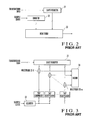
- Fig. 2 shows a digital filter circuit of the first prior art.
- a shift register 21 temporarily stores input 1-bit transmission data and outputs it to a ROM table 23.
- a counter 22 counts input sample clocks and outputs the obtained count value to the ROM table 23.
- the ROM table 23 outputs a filter output waveform, which is stored in advance and corresponds to the input data sequence, on the basis of the outputs from the shift register 21 and counter 22.
- This prior-art digital filter circuit is disclosed in Japanese Patent Laid-Open No. 63-69310.
- Fig. 3 shows a digital filter circuit of the second prior art.
- a shift register 31 serially receives transmission data of a plurality of bits and parallelly outputs the bit signals to multipliers 33-1 to 33-n.
- a counter 32 counts input sample clocks and outputs TAP coefficients corresponding to the count value to the multipliers 33-1 to 33-n.
- the multipliers 33-1 to 33-n weight the respective bit signals of the parallel outputs from the shift register 31 using the TAP coefficients and then outputs the bit signals to an adder 34.
- a digital filter circuit when the ROM table lookup filter shown in Fig. 2 is used, a digital filter circuit can easily be constituted. Generally, however, no ROM table lookup filter can be used for a multilevel signal containing a plurality of input bits. Hence, the normal FIR (inFinite Impulse Response) filter is normally used. However, since this circuit requires a number of multipliers, the circuit scale becomes large.
- FIR inFinite Impulse Response
- a digital filter circuit comprising decoding means for decomposing an input multilevel signal into a plurality of 1-bit signals, a plurality of ROM tables which output filter waveforms stored in advance, on the basis of the 1-bit signals output from the decoding means, and weighting and addition means for executing a plurality of weighting operations for respective bits of outputs from the ROM tables and then adding the outputs.
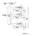
- Fig. 1 shows a digital filter circuit according to an embodiment of the present invention.
- a decoder 11 decomposes an input multilevel signal containing a plurality of bits into a plurality of 1-bit signals and outputs the 1-bit signals to shift registers 12-1, 12-2,..., 12-n.
- the shift registers 12-1, 12-2,..., 12-n serial/parallel-convert the 1-bit signals from the decoder 11 and output the 1-bit signals to ROM tables 13-1, 13-2,..., 13-n, respectively.
- a counter 15 counts sample clocks and outputs the count value to the ROM tables 13-1, 13-2,..., 13-n.
- the ROM tables 13-1, 13-2,..., 13-n output filter output waveforms, which are stored in advance and correspond to the input data sequence, to multipliers 14-1, 14-2,..., 14-n, respectively, on the basis of the outputs from the shift registers 12-1, 12-2,..., 12-n and the outputs from the counter 15.
- the adder 16 adds and outputs the outputs from the multipliers 14-1, 14-2,..., 14-n.
- a digital filter which receives a multilevel signal in which a ROM table lookup filter receives a multilevel signal containing a plurality of bits, will be described.
- the input multilevel signal is decomposed into a plurality of 1-bit signals by the decoder 11.
- the 1-bit signals are input to the ROM tables 13-1, 13-2,..., 13-n through the shift registers 12-1, 12-2,..., 12-n.
- ROM tables 13-1, 13-2,..., 13-n outputs that are preset and correspond to the input data sequences are read out on the basis of the outputs from the shift registers 12-1, 12-2,..., 12-n and the outputs from the counter 15.
- the respective bits of the outputs from the ROM tables 13-1, 13-2,..., 13-n are weighted by the multipliers 14-1, 14-2,..., 14-n and added by and output from the adder 16.
- the multilevel signal sequence containing a plurality of bits that construct input transmission data is decomposed by the decoder 11 into binary signal sequences formed from 1-bit signals of N sequence.
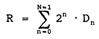
- R be the value of the input signal
- Dn be the nth signal obtained by the decomposition.
- the input signal sequence is so decomposed as to satisfy
- Outputs Fn from the ROM tables 13-1, 13-2,..., 13-n are weighted by the multipliers 14-1, 14-2,..., 14-in in accordance with equation (2) below and added by and output from the adder 16.
- G is the output from the adder 16.
- Dn ⁇ 1.
- a table used in a normal ROM lookup filter can be directly used as the data table of each ROM table.
- the input signal R may be expressed by offset binary data. Each bit of the binary signal may be decoded to obtain a signal sequence.
- a ROM table corresponding to an input value "+1" or "0" may be used.
- the input signal R is expressed by offset binary data, and each bit of the offset binary signal is used as a signal sequence obtained by decoding.
- the data table of the ROM table is different from that of a normal ROM lookup filter.
- a normal ROM lookup filter always processes an input value as "+1” or "-1".
- a table is prepared as convolution of an impulse response for an input signal sequence having a value "+1" or "-1". In the method of the present invention, however, since an input value is "+1" or "0", a corresponding table must be prepared.
- a ROM table can be used even for a multilevel input signal. For this reason, the circuit scale can be greatly reduced as compared to a conventional FIR filter.
Landscapes
- Engineering & Computer Science (AREA)
- Physics & Mathematics (AREA)
- Computer Hardware Design (AREA)
- Mathematical Physics (AREA)
- Computing Systems (AREA)
- Theoretical Computer Science (AREA)
- Filters That Use Time-Delay Elements (AREA)
- Cable Transmission Systems, Equalization Of Radio And Reduction Of Echo (AREA)
- Analogue/Digital Conversion (AREA)
- Compression, Expansion, Code Conversion, And Decoders (AREA)
Abstract
Description


Claims (7)
- A digital filter circuit characterized by comprising:decoding means (11) for decomposing an input multilevel signal into a plurality of 1-bit signals;a plurality of ROM tables (13-1 - 13-n) which output filter waveforms stored in advance, on the basis of the 1-bit signals output from said decoding means; andweighting and addition means (14-1 - 14-n, 16) for executing a plurality of weighting operations for respective bits of outputs from said ROM tables and then adding the outputs.
- A circuit according to claim 1, wherein letting R be an input signal and Dn be an nth signal obtained by decomposition when an input multilevel signal sequence containing a plurality of bits is decomposed into binary signal sequences formed from 1-bit signals of N sequence, said decoding means performs decomposing operation so as to satisfy
- A circuit according to claim 2, wherein letting G be an output from said weighting and addition means and Fn be the output from said ROM table in correspondence with each signal sequence obtained by decomposition, said weighting and addition means performs weighting and adding operation in accordance with

- A circuit according to claim 2, wherein in decoding the input signal R into the nth signal Dn, said decoding means decodes the input signal R so as to satisfy Dn = ±1.
- A circuit according to claim 2, wherein
in decoding the input signal R to the nth signal Dn, said decoding means expresses the input signal R by offset binary data and outputs a signal sequence obtained by decoding each bit of the binary data, and
said ROM table corresponds to an input value "+1" or "0". - A circuit according to claim 1, wherein said weighting and addition means comprises
multipliers (14-1 - 14-n) which multiply the outputs from said ROM tables by weighting signals for respective bits, and
an adder (16) which adds outputs from said multipliers. - A digital filter circuit characterized by comprising:a decoder (11) which decomposes an input multilevel signal containing a plurality of bits into 1-bit signals and outputs the 1-bit signals;a plurality of shift registers (12-1 - 12-n) which receives the 1-bit signals from said decoder;a counter (15) which counts input sample clocks and outputs count values;a plurality of ROM tables (13-1 - 13-n) which output filter waveforms that are stored in advance and correspond to input data sequences on the basis of the outputs from said shift registers and counter;multipliers (14-1 - 14-n) which weight respective bits of outputs from said ROM tables in correspondence with the bit outputs from said decoder; andan adder (16) which adds the outputs from said multipliers.
Applications Claiming Priority (2)
| Application Number | Priority Date | Filing Date | Title |
|---|---|---|---|
| JP2001236697A JP2003046374A (en) | 2001-08-03 | 2001-08-03 | Digital filter circuit |
| JP2001236697 | 2001-08-03 |
Publications (2)
| Publication Number | Publication Date |
|---|---|
| EP1282228A2 true EP1282228A2 (en) | 2003-02-05 |
| EP1282228A3 EP1282228A3 (en) | 2005-08-10 |
Family
ID=19067919
Family Applications (1)
| Application Number | Title | Priority Date | Filing Date |
|---|---|---|---|
| EP02017383A Withdrawn EP1282228A3 (en) | 2001-08-03 | 2002-08-02 | Digital filter circuit |
Country Status (3)
| Country | Link |
|---|---|
| US (1) | US7068713B2 (en) |
| EP (1) | EP1282228A3 (en) |
| JP (1) | JP2003046374A (en) |
Cited By (1)
| Publication number | Priority date | Publication date | Assignee | Title |
|---|---|---|---|---|
| RU2693595C1 (en) * | 2018-03-15 | 2019-07-03 | Федеральное государственное бюджетное образовательное учреждение высшего образования "Юго-Западный государственный университет" (ЮЗГУ) | Method of phase referencing generated pulse train to external trigger pulse |
Families Citing this family (5)
| Publication number | Priority date | Publication date | Assignee | Title |
|---|---|---|---|---|
| US7787520B2 (en) * | 2004-10-06 | 2010-08-31 | Broadcom Corporation | Method and system for channel estimation in a single channel (SC) single-input multiple-output (SIMO) system |
| US7873101B2 (en) * | 2005-03-25 | 2011-01-18 | Broadcom Corporation | Low latency digital filter and method |
| JP4217787B2 (en) * | 2005-06-15 | 2009-02-04 | 国立大学法人東京工業大学 | Signal processing method and signal processing apparatus |
| JP2007336474A (en) * | 2006-06-19 | 2007-12-27 | Handotai Rikougaku Kenkyu Center:Kk | Signal processing method, and signal processing apparatus |
| US10019234B2 (en) | 2015-10-05 | 2018-07-10 | Altera Corporation | Methods and apparatus for sequencing multiply-accumulate operations |
Family Cites Families (13)
| Publication number | Priority date | Publication date | Assignee | Title |
|---|---|---|---|---|
| DE3579591D1 (en) * | 1984-11-22 | 1990-10-11 | Devon County Council | DATA MODULATOR DEMODULATOR SYSTEM. |
| JPS61171215A (en) | 1985-01-25 | 1986-08-01 | Nec Corp | Band limit filter |
| JPS62295506A (en) | 1986-06-16 | 1987-12-22 | Toshiba Corp | Digital filter circuit |
| JPS6369310A (en) | 1986-09-11 | 1988-03-29 | Nec Corp | Digital filter |
| US4775851A (en) * | 1987-06-01 | 1988-10-04 | Motorola, Inc. | Multiplierless decimating low-pass filter for a noise-shaping A/D converter |
| JP2774501B2 (en) * | 1987-11-05 | 1998-07-09 | 株式会社リコー | Multi-level gradation processing method for color image |
| JPH04100403A (en) | 1990-08-20 | 1992-04-02 | Fujitsu Ltd | Binary transversal filter |
| DE69024213T2 (en) * | 1990-09-18 | 1996-07-04 | Alcatel Nv | Multi-channel clock frequency reducer |
| JPH06104694A (en) | 1992-09-22 | 1994-04-15 | Sony Corp | Digital filter |
| US5838725A (en) | 1996-12-06 | 1998-11-17 | U.S. Philips Corporation | Floating point digital transversal filter |
| WO2000062421A1 (en) | 1999-04-14 | 2000-10-19 | Nokia Networks Oy | Digital filter and method for performing a multiplication based on a look-up table |
| DE19919367A1 (en) | 1999-04-28 | 2000-12-07 | Siemens Ag | Code-multiplex signal transmission |
| EP1113580B1 (en) | 1999-12-28 | 2015-02-25 | Hitachi Kokusai Electric Inc. | Coder with error correction, decoder with error correction and data transmission apparatus using the coder and decoder |
-
2001
- 2001-08-03 JP JP2001236697A patent/JP2003046374A/en active Pending
-
2002
- 2002-07-29 US US10/206,673 patent/US7068713B2/en not_active Expired - Fee Related
- 2002-08-02 EP EP02017383A patent/EP1282228A3/en not_active Withdrawn
Cited By (1)
| Publication number | Priority date | Publication date | Assignee | Title |
|---|---|---|---|---|
| RU2693595C1 (en) * | 2018-03-15 | 2019-07-03 | Федеральное государственное бюджетное образовательное учреждение высшего образования "Юго-Западный государственный университет" (ЮЗГУ) | Method of phase referencing generated pulse train to external trigger pulse |
Also Published As
| Publication number | Publication date |
|---|---|
| JP2003046374A (en) | 2003-02-14 |
| US20030033337A1 (en) | 2003-02-13 |
| US7068713B2 (en) | 2006-06-27 |
| EP1282228A3 (en) | 2005-08-10 |
Similar Documents
| Publication | Publication Date | Title |
|---|---|---|
| US6243729B1 (en) | Digital finite-impulse-response (FIR) filter with a modified architecture based on high order Radix-N numbering | |
| JPH0435213A (en) | filter circuit | |
| GB2214386A (en) | Signal equaliser | |
| US5191547A (en) | Decimating digital finite impulse response filter | |
| EP1282228A2 (en) | Digital filter circuit | |
| US8161092B2 (en) | Method and apparatus for efficient matrix multiplication in a direct sequence CDMA system | |
| US7945610B2 (en) | Convolution operation circuit | |
| EP1703637A2 (en) | Digital finite impulse response filter | |
| EP0990305B1 (en) | System for varying the dynamic range of coefficients in a digital filter | |
| EP0464666B1 (en) | Input-weighted transversal filter | |
| US4800517A (en) | Word-sliced signal processor | |
| US7139341B2 (en) | Receiver circuit for a communications terminal and method for processing signals in a receiver circuit | |
| US7167514B2 (en) | Processing of quinary data | |
| KR100280497B1 (en) | Discrete Wavelet Converter of Grid Structure | |
| US4931973A (en) | Method of generating updated transversal filter coefficients | |
| US6985522B2 (en) | Variable-gain digital filter | |
| US5956262A (en) | Digital filtering device | |
| EP0426296B1 (en) | Apparatus having modular interpolation architecture | |
| KR100526074B1 (en) | Apparatus and method for equalizer filter units responsive to 5-level inputs signals | |
| US5130942A (en) | Digital filter with front stage division | |
| KR100850703B1 (en) | A device for determining the rank of the sample, an apparatus for determining the rank of the plurality of samples, and an ith rank order filter | |
| US20020010727A1 (en) | Area efficient fir filter with programmable coefficients | |
| SU1661968A1 (en) | Digital filter with multilevel delta modulation | |
| EP1047221B1 (en) | PN code generator, communication unit using the PN code generator, communication system, and PN code generation method | |
| KR0155263B1 (en) | Multi-division digital filter |
Legal Events
| Date | Code | Title | Description |
|---|---|---|---|
| PUAI | Public reference made under article 153(3) epc to a published international application that has entered the european phase |
Free format text: ORIGINAL CODE: 0009012 |
|
| AK | Designated contracting states |
Designated state(s): AT BE BG CH CY CZ DE DK EE ES FI FR GB GR IE IT LI LU MC NL PT SE SK TR |
|
| AX | Request for extension of the european patent |
Extension state: AL LT LV MK RO SI |
|
| PUAL | Search report despatched |
Free format text: ORIGINAL CODE: 0009013 |
|
| AK | Designated contracting states |
Kind code of ref document: A3 Designated state(s): AT BE BG CH CY CZ DE DK EE ES FI FR GB GR IE IT LI LU MC NL PT SE SK TR |
|
| AX | Request for extension of the european patent |
Extension state: AL LT LV MK RO SI |
|
| 17P | Request for examination filed |
Effective date: 20050722 |
|
| AKX | Designation fees paid |
Designated state(s): DE FR GB |
|
| STAA | Information on the status of an ep patent application or granted ep patent |
Free format text: STATUS: THE APPLICATION HAS BEEN WITHDRAWN |
|
| 18W | Application withdrawn |
Effective date: 20060412 |