EP1282137A1 - Redundancy circuit and method for replacing defective memory cells in a flash memory device - Google Patents
Redundancy circuit and method for replacing defective memory cells in a flash memory device Download PDFInfo
- Publication number
- EP1282137A1 EP1282137A1 EP02255361A EP02255361A EP1282137A1 EP 1282137 A1 EP1282137 A1 EP 1282137A1 EP 02255361 A EP02255361 A EP 02255361A EP 02255361 A EP02255361 A EP 02255361A EP 1282137 A1 EP1282137 A1 EP 1282137A1
- Authority
- EP
- European Patent Office
- Prior art keywords
- memory cells
- regular
- column
- columns
- main column
- Prior art date
- Legal status (The legal status is an assumption and is not a legal conclusion. Google has not performed a legal analysis and makes no representation as to the accuracy of the status listed.)
- Granted
Links
Images

Classifications
-
- G—PHYSICS
- G11—INFORMATION STORAGE
- G11C—STATIC STORES
- G11C29/00—Checking stores for correct operation ; Subsequent repair; Testing stores during standby or offline operation
- G11C29/70—Masking faults in memories by using spares or by reconfiguring
- G11C29/78—Masking faults in memories by using spares or by reconfiguring using programmable devices
- G11C29/80—Masking faults in memories by using spares or by reconfiguring using programmable devices with improved layout
- G11C29/808—Masking faults in memories by using spares or by reconfiguring using programmable devices with improved layout using a flexible replacement scheme
-
- G—PHYSICS
- G11—INFORMATION STORAGE
- G11C—STATIC STORES
- G11C29/00—Checking stores for correct operation ; Subsequent repair; Testing stores during standby or offline operation
- G11C29/70—Masking faults in memories by using spares or by reconfiguring
- G11C29/78—Masking faults in memories by using spares or by reconfiguring using programmable devices
- G11C29/80—Masking faults in memories by using spares or by reconfiguring using programmable devices with improved layout
- G11C29/81—Masking faults in memories by using spares or by reconfiguring using programmable devices with improved layout using a hierarchical redundancy scheme
Definitions
- Flash EPROMs A third type of memory has more recently gained popularity.
- This type of memory flash EPROMs
- Flash memory cells can be individually programmed utilizing the hot carrier effect in the same way as EPROM cells are programmed. Flash memory cells are also electrically erasable by the tunnel effect.
- the memory cells of a flash EPROM memory includes a floating-gate transistor that has an oxide layer whose thickness is greater than the oxide layer thickness of an EEPROM floating gate transistor but smaller than the oxide layer thickness of an EPROM floating gate transistor. Consequently, the flash memory cell is capable of erasure by the tunnel effect.
- flash memory device 1 includes redundant circuitry for efficiently replacing columns of memory cells 20 having a defect.
- Flash memory device 1 includes one or more arrays or banks 2 of memory cells 20.
- Each array 2 of memory cells 20 may be arranged into rows and columns 16 of memory cells 20.
- each array 2 is partitioned into sectors 3 of memory cells 20, with multiple sectors 3 being grouped into one or more blocks 30 of memory cells 20.
- Each block 30 of memory cells 20 may include a plurality of redundant columns 4 of redundant memory cells 20.
- Each redundant column 4 of redundant memory cells 20 may be capable of replacing any of a plurality of regular (i.e., non-redundant) columns 16 of memory cells 20 in the block 30 in which the redundant column 4 is disposed, as discussed in greater detail below.
- array 2 is illustrated in Figure 2 as being divided into two or more sectors 3 of memory cells 20 that may form one or more blocks 30, it is understood that array 2 may be divided into more than two sectors 3 and blocks 30 of memory cells 20.
- Replacement of all of the columns 16 associated with a main column line 50 may be chosen, for example, upon the existence of a cluster of defects that shorts a local column line 5 with a main column line 50 together, or main column lines 50 together.
- the value stored in fifth sub-set 11e may be seen as determining whether an addressed main column line 5 (and its corresponding regular columns 16) is replaced entirely or only with respect to a single block.
- Flash memory device 1 may further include redundancy decode circuitry 18 coupled to receive the output of each sense amplifier 9 and selectively replace the output of one or more sense amplifiers 9a associated with a defective column 16 with the output of one or more sense amplifiers 9b associated with redundant columns 4.
- Redundancy decode circuitry 18 may be implemented, for example, with multiplexing circuitry to effectively replace the output of one or more sense amplifiers 9a with the output of one or more sense amplifiers 9b.
- Redundancy decode circuitry 18 replaces the output of a sense amplifier 9a with the output of a sense amplifier 9b based upon the contents of secondary array 10.
- Redundancy decode circuitry 18 is implemented to replace the output of one or more sense amplifiers 9a with the output of one or more sense amplifier 9b, in order to minimize the timing of a memory read operation and/or maintain the timing of a memory read operation within acceptable limits. It is understood, however, that redundancy decode circuitry 18 may be implemented between column decode circuitry 8 and sense amplifiers 9 and/or otherwise made part of column decode circuitry 8. In this alternative implementation, redundancy decode circuitry 18 selectively replaces one or more column lines 5 associated with one or more defective regular columns 16 with one or more column lines 5 associated with one or more redundant columns 4 of memory cells. The output of redundancy decode circuitry 18 would, in this case, be connected to the input of sense amplifiers 9. In either implementation, the net effect is that defective columns 16 of memory cells are replaced with a redundant column 4 of memory cells based upon the contents of secondary array 10.
- Flash memory device 1 may further include a redundancy control circuit 12 for generally performing replacements of defective regular columns 16 during a memory access operation based upon the contents of secondary array 10.
- redundancy control circuit 12 examines each set 11 of memory cells in secondary array 10 during a memory access operation to see if a regular column 16 or group thereof is identified for replacement by a set 11.
- redundancy control circuit 12 initiates _a replacement of one of more regular columns 16.
- the replacement may be a single regular column 16 or one or more groups of columns 16 associated with a main column line 50.
- the column address (and/or main column line 50) and block address corresponding to a regular column 16 (main column line 50) in the sector 3 are stored in sub-sets 11a and 11b, respectively, of any set 11 in secondary array 10.
- Sub-set 11c is loaded with a value, such as a logic one, to indicate that the set 11 now obtains column replacement information.
- Sub-set 11d is set to a value, such as logic zero, to indicate that at least one group of regular columns 16 is to be replaced, instead of a single column 16 of memory cells 20.
- a value such as a logic one value, is stored sub-set 11e of the chosen set 11 so as to indicate that the main column line 50 (identified in sub-set 11a) and all of the regular columns 16 associated therewith are to be replaced.
- the chosen set 11 is fully programmed to facilitate the replacement of all of the regular columns 16 associated with the addressed main column line 50 during a memory read operation.
- steps 40 and 41 may be performed by the manufacturer before delivery of the flash memory device 1 to a user.
- redundancy control circuit 12 controls at 46 redundancy decode circuitry 18 so that the output of sense amplifiers 9a associated with addressed columns 16 that are defect-free are connected to data I/O circuit 13, together with the output of sense amplifiers 9b associated with the particular redundant column 4 identified during step 45.
- control circuit 10 controls redundancy decode circuitry 18 so that the particular redundant column 4 identified by secondary array 2 replaces the corresponding defective column 16 at 45. Thereafter, the output of redundancy decode circuitry 18 is available to data I/O circuit 13 for driving the external data I/O pins 14 accordingly, thereby completing the memory read operation.
- redundancy control circuit 12 controls at 51 redundancy decode circuitry 18 so that the output of sense amplifiers 9a associated with addressed regular columns 16 that are defect-free are connected to data I/O circuit 13, together with the output of sense amplifiers 9b associated with the particular redundant column 4 identified during step 50.
- redundancy control circuit 12 controls redundancy decode circuitry 18 so that the particular redundant columns 4 identified by secondary array 10 replaces the corresponding defective columns 16 at 49. Thereafter, the output of redundancy decode circuitry 18 is available to data I/O circuit 13 for driving the external data I/O pins 14 accordingly, thereby completing the memory read operation.
- the flash memory device 1 may increase the repair probability without increasing the number of groups 11 in secondary array 10. For instance, if the size of the blocks are halved (i.e., the number of blocks in array 2 are doubled), the repair probability increases. The only real effect the halving of the blocks has on secondary array 2 is that each group 11 in secondary array 2 must now include an additional bit for identifying the addressed block. As a result, the repair probability of flash memory device 1 may be increased without a substantial increase in the size of secondary array 10.
Landscapes
- For Increasing The Reliability Of Semiconductor Memories (AREA)
- Read Only Memory (AREA)
Abstract
Description
- The present invention relates to a redundancy technique for nonvolatile memory devices, and particularly to a circuit and method for replacing defective memory cells in a nonvolatile memory device based upon the type of defect.
- The first nonvolatile memories were electrically programmable read-only memories (EPROMs). In these memories, the memory cells include a floating-gate transistor that is programmable using the hot carrier effect. Programming of an EPROM memory cell includes applying a potential difference between the drain and the source of the floating gate transistor in the presence of a high potential difference (of about 20 volts, this value varying according to the desired programming speed) between the control gate and the source. The application of the first of these potential differences generates an electrical field that gives rise to a flow of electrons in the channel. These electrons collide with atoms of the channel, causing the appearance of new free electrons. These electrons have very high energy (hence the term "hot carriers"). The high difference in potential between the control gate and the source of the floating gate transistor gives rise to a strong electrical field between the floating gate and the substrate, the effect of which is that certain of these electrons are injected into the floating gate, thus putting the memory cell in a state known as a "programmed" state.
- The fact that the programming of a memory cell requires the application of voltages both to the control gate and to the drain of the floating-gate transistor eliminates the need for the use of a selection transistor to program one particular memory cell without programming the others. This results in a relatively small silicon area and the effectuation of large scale integration . By contrast, the erasure of all the memory cells of the memory is done substantially simultaneously by exposing the memory cells to ultraviolet radiation.
- In addressing the need to individually erase EPROM memory cells, electrically erasable programmable read only memories (EEPROMs) were created. These memories are electrically programmable and erasable by tunnel effect (i.e., the Fowler Nordheim effect). The memory cells have a floating-gate transistor whose drain is connected to the bit line by a selection transistor. The gate of the selection transistor is connected to the word line. The gate of the floating-gate transistor is controlled by a bias transistor. Generally, the source of the floating gate transistor is connected to a reference potential, such as ground. These floating-gate transistors have an oxide layer between the substrate and the floating gate that is very thin to enable the transfer of charges by tunnel effect. The advantage of EEPROMs as compared with EPROMs lies in the fact that each memory cell is programmable and erasable independently of the other EEPROM cells. The tradeoff here is that a larger surface area of silicon is required and therefore a smaller scale of integration is achieved.
- A third type of memory has more recently gained popularity. This type of memory, flash EPROMs, combines the relatively high integration of EPROMs with the ease of programming and erasure of EEPROMs. Flash memory cells can be individually programmed utilizing the hot carrier effect in the same way as EPROM cells are programmed. Flash memory cells are also electrically erasable by the tunnel effect. The memory cells of a flash EPROM memory includes a floating-gate transistor that has an oxide layer whose thickness is greater than the oxide layer thickness of an EEPROM floating gate transistor but smaller than the oxide layer thickness of an EPROM floating gate transistor. Consequently, the flash memory cell is capable of erasure by the tunnel effect. For erasure, a highly negative potential difference is created between the control gate and the source of the floating gate transistor, the drain being left in the high impedance state or connected to the ground potential so that a high electrical field is created which tends to remove the electrons from the floating gate.
- Referring to Figure 1, flash EPROM devices, hereinafter referred to as flash memory devices, typically include at least one array A of flash memory cells organized into rows and columns of flash memory cells. Array A is typically partitioned into blocks B, each of which is further divided into sectors S. Each column of memory cells is coupled to a distinct local column line. Array A typically includes a plurality of main column lines. A plurality of local column lines are selectively connected to each main column line. Each local column line is connected to a distinct column of memory cells. Having the columns of memory cells and local column lines divided into sectors allows for erase operations to be performed on sectors of memory cells. Main column lines are also used to route a signal appearing on a local column line to the periphery of array A without an appreciable time delay or signal degradation. The use of local and main column lines in flash memory devices is known in the art.
- A row decoder R and column decoder C are used to select a single row and at least one column of memory cells based upon the value of an externally generated address applied to the flash memory device. Sense amplifiers SA are coupled to the main column lines to amplify the voltage levels on the addressed column lines corresponding to the data values stored in the addressed flash memory cells. The particular implementations of array A, the row and column decoders and sense amplifiers SA are known in the art and will not be described further for reasons of simplicity.
- Redundancy has been previously utilized in flash memory devices to, among other things, replace columns of memory cells having a defect with redundant columns of memory cells so as to improve manufacturing yield. Redundant columns RC are disposed in or immediately adjacent each block B. Each block B has a distinct set of redundant columns RC, as shown in Figure 1. A redundant column RC is adapted to replace a column of flash memory cells having a defect (i.e., a defective column) in the block B with which redundant column RC is associated. Nonvolatile storage components SC, which may be maintained in a secondary array of memory cells, are utilized to identify whether the redundant columns RC are used to replace a defective column.
- In one existing flash memory design, defective regular columns of memory cells are individually replaced with redundant columns of memory cells. A single storage component SC is associated with a distinct redundant column RC. Each storage component SC is capable of storing the column address of the defective column that the associated redundant column RC replaces, together with an enable bit to enable the column replacement during a memory access operation. This type of existing flash memory device is thereby capable of individually replacing defective columns in the flash memory array A with redundant columns of redundant memory cells. This existing redundancy strategy is more efficient in overcoming random failures appearing in array A, and is less efficient in overcoming clusters of failures therein.
- In another existing flash memory design, main column lines and the columns of memory cells associated therewith are replaced as a set. Specifically, a storage component is capable of identifying for replacement a main column line and columns of memory cells associated therewith in a single block, together with an enable bit to enable the replacement during a memory access operation. This type of existing flash memory device is thereby capable of replacing defective columns in a set with a set of redundant columns RC of redundant memory cells. This existing redundancy strategy is more efficient in overcoming clusters of failures appearing in array A and less efficient in handling random failures in array A. Both of the above-described existing flash memory designs are relatively inflexible in that the storage components SC in each case are only available for efficiently overcoming a certain type of defect.
- In addition to each of the above-described redundancy schemes being limited in efficiently replacing different types of defects, the ability of the above-described existing flash memory devices to replace defective columns of memory cells is limited as the number of defective columns increases. This reduced inability is due in part to the fact that the maximum number of redundant columns that can be used in a single word is equal to the number of sense amplifiers SAR used for sense amplification of the redundant columns RC. The reduced inability is also due to the fact that the maximum number of defective columns that can be replaced in any block B is equal to the number of redundant columns RC in a block B.
- Based upon the foregoing, there is a need to more efficiently replace defective columns in flash memory devices.
- Embodiments of the present invention overcome shortcomings in prior flash memory devices and satisfy a significant need for a flash memory device having improved repair probability for the redundant circuitry provided. According to a first exemplary embodiment of the present invention, a flash memory device includes sets of secondary storage elements, each of which is not rigidly associated with a single redundant column or main column line in a block of memory cells. Instead, each set of secondary storage elements is capable of identifying for replacement a column or at least one group thereof. In this way, the number of sets of secondary storage elements is not fixed to the number of redundant columns/main column lines and is instead based upon the maximum number of replacements that is desired to be replaced. Consequently, the repair probability is enhanced.
- Each set of storage elements is capable of storing information identifying any of a regular (i.e., non-redundant) column of memory cells and a main column line in a block of memory cells as being defective. The flash memory device may further include redundancy circuitry for selectively replacing, during a memory read operation, any of a regular column of memory cells in a block and a main column line together with the corresponding regular columns of memory cells coupled thereto, based upon the information stored in a set of storage elements.
- In addition or in the alternative, each set of storage elements is capable of storing information identifying for replacement a main column line and regular columns of memory cells associated therewith, and identifying whether the identified regular columns of memory cells are regular columns in a single block or in multiple blocks. The redundancy circuitry cooperates with the sets of storage elements to selectively replace, during a memory read operation, the identified main column line and identified regular columns associated therewith based upon the information stored in the at least one set of storage elements
- An exemplary flash memory device includes at least one array of memory cells arranged into rows and columns and partitioned into a plurality of sectors of memory cells grouped into blocks, such that each block of memory cells includes a plurality of redundant columns of memory cells. Address decode circuitry receives an externally-generated address and selects a row and at least one column of memory cells corresponding to the externally-generated address. The exemplary flash memory device further includes a secondary memory array having the plurality of sets of secondary storage elements located therein. The redundancy circuitry examines each set of secondary storage elements, selects a redundant column of memory cells, and replaces an addressed column with the selected, redundant column of memory cells, upon an affirmative determination that a set of secondary storage elements in the secondary memory array identifies the addressed column as being defective. Upon an affirmative determination that a set of secondary storage elements in the secondary memory array identifies an addressed regular column and other regular columns in a block that are associated with a main column line as being defective, the redundancy circuitry selects a main column line associated with redundant columns. Thereafter, the redundancy circuitry replaces the main column line and the defective column lines associated therewith with the selected main column and redundant columns
- A more complete understanding of the system and method of the present invention may be obtained by reference to the following Detailed Description when taken in conjunction with the accompanying Drawings wherein:
- Figure 1 is a block diagram of a known flash memory device;
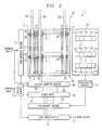
- Figure 2 is a block diagram of a flash memory device according to an exemplary embodiment of the present invention;
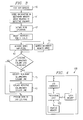
- Figure 3 is a flow chart illustrating an operation of the exemplary flash memory device of Figure 2; and
- Figure 4 is a block diagram of a computing/communications device having therein the flash memory device of Figure 2.
-
- The present invention will now be described more fully hereinafter with reference to the accompanying drawings in which an exemplary embodiment of the invention is shown. This invention may, however, be embodied in many different forms and should not be construed as being limited to the embodiment set forth herein. Rather, the embodiment is provided so that this disclosure will be thorough and complete, and will fully convey the scope of the invention to those skilled in the art.
- Referring to Figure 2, there is shown a nonvolatile memory device 1 according to an exemplary embodiment of the present invention. Although it is understood that the nonvolatile memory device 1 may be virtually any type of nonvolatile memory device, nonvolatile memory device 1 will be described below as a bi-level flash memory device for reasons of simplicity.
- In general terms, flash memory device 1 includes redundant circuitry for efficiently replacing columns of
memory cells 20 having a defect. Flash memory device 1 includes one or more arrays or banks 2 ofmemory cells 20. Each array 2 ofmemory cells 20 may be arranged into rows andcolumns 16 ofmemory cells 20. According to the exemplary embodiment of the present invention, each array 2 is partitioned intosectors 3 ofmemory cells 20, withmultiple sectors 3 being grouped into one ormore blocks 30 ofmemory cells 20. Eachblock 30 ofmemory cells 20 may include a plurality ofredundant columns 4 ofredundant memory cells 20. Eachredundant column 4 ofredundant memory cells 20 may be capable of replacing any of a plurality of regular (i.e., non-redundant)columns 16 ofmemory cells 20 in theblock 30 in which theredundant column 4 is disposed, as discussed in greater detail below. Although array 2 is illustrated in Figure 2 as being divided into two ormore sectors 3 ofmemory cells 20 that may form one ormore blocks 30, it is understood that array 2 may be divided into more than twosectors 3 and blocks 30 ofmemory cells 20. - Array 2 is shown in Figure 2 as being relatively sparsely populated with
memory cells 20 for reasons of clarity. It is understood that array 2 is substantially entirely populated withmemory cells 20, arranged in rows and columns ofmemory cells 20 as described above. - Within each
sector 3 of a block, alocal column line 5 may be connected to a distinctregular column 16 orredundant column 4 of memory cells. In addition, array 2 includes a plurality ofmain column lines 50 which extend substantially from one side of array 2, such as the top side, to an opposed side thereof. Becausecolumns 16 of memory cells are disposed withinsectors 3 so as to effectuate erase operations ofmemory cells 20 at the sector level,main column lines 50 are utilized to route addressed memory cells to the periphery of array 2. Eachmain column line 50 is coupled to a plurality ofcolumn lines 5 such that any associated column line 5 (and its corresponding column of memory cells) may be connected to amain column line 50 during a memory access operation. -
Local columns 16 indifferent sectors 3 of the same block and having the same address within theirrespective sectors 3 are replaced by a singleredundant column 4. - The
redundant columns 4 of each block ofmemory cells 20 are adapted to replace defectiveregular columns 16 ofmemory cells 20 according to a predetermined replacement scheme. For instance, both theregular columns 16 and theredundant columns 4 in a block may be each divided into one or more sets, with each set ofredundant columns 4 being capable of replacingcolumns 16 in a distinct set of regular columns. The particularredundant column 4 of a set of redundant columns that selectively replaces a defectiveregular column 16 of a set of columns in a block may be based upon the column address of the defectiveregular column 16. In particular, a portion of the column address of the column(s) to be replaced is used to identify the particular redundant column(s) 4 in the corresponding set ofredundant columns 4 to be used in a column replacement. In this way, for a regular given column(s) 16 to be replaced, the redundant column(s) 4 that may selectively used in the replacement may be substantially quickly and simply determined. - Flash memory device 1 may further include
row decode circuitry 7 which receives an externally generated address or portion thereof and selects and/or activates a row ofmemory cells 20 in asector 3. In particular, the row ofmemory cells 20 corresponding to the externally generated address is selected and/or activated by being connected tocolumn lines 5. Rowdecode circuitry 7 may include logic that, for example, in response to receiving an externally generated address, drives asingle row line 6 corresponding to the externally generating address to a first voltage level to activate each memory cell in the row, while driving the remainingrow lines 6 to another voltage level to deactivate thememory cells 20 in the remaining rows. Rowdecode circuitry 7 may be implemented with boolean logic gates as is known in the art. - Further, flash memory device 1 may include
column decode circuitry 8 which receives an externally generated address and selects one ormore columns 16 corresponding to the externally generated address.Column decode circuitry 8 may, for example, be implemented as multiplexing circuitry connected to eachcolumn line 5 in array 2 for connecting, based upon the received address, thecolumn lines 5 associated with the addressedcolumns 16 to their correspondingmain column lines 50 and for selecting such main column lines 50. In this way, thelocal column lines 5 associated with the addressedcolumns 16, having the data values from the addressedmemory cells 20, are provided externally to array 2 for subsequent amplification.Column decode circuitry 8 may includedecode circuitry 8a for selecting one or morelocal column lines 5 associated with the addressedcolumns 16 as described above, andredundant decode circuitry 8b for selecting one ormore column lines 5 associated withredundant columns 4 ofredundant memory cells 20.Column decode circuitry 8b connects thecolumn line 5 of one or moreredundant columns 4 to redundantmain column lines 50 so that data values from selectedredundant memory cells 20 are provided externally to array 2 for subsequent amplification. - During a memory read operation, addressed
memory cells 20 are connected to themain column lines 50 corresponding thereto, as explained above. Typically, the connection of the addressedmemory cells 20 to their correspondingmain column lines 50 results in themain column lines 50 being at one of two voltage levels. Flash memory device 1 may includesense amplifiers 9 that sense the voltage levels on themain column lines 50 corresponding to the data stored in the addressedmemory cells 20 and drive output signals of thesense amplifiers 9 to voltage levels that are more easily interpreted or otherwise handled by circuitry external to array 2.Sense amplifiers 9 may includesense amplifiers 9a coupled tomain column lines 50 ofregular columns 16, andsense amplifiers 9b coupled tomain column lines 5 ofredundant columns 4. - Flash memory device 1 may include a data input/output (I/O)
circuit 13 that generally couples addressedmemory cells 20 to external I/O data pins 14 of flash memory device 1. As shown in Figure 2, data I/O circuit 13 is coupled to the output ofsense amplifiers 9. Flash memory device 1 may also includecontrol circuitry 15 for receiving externally generated, input control signals and controlling the various components of flash memory device 1 (row decode circuitry 7,column decode circuitry 8,sense amplifiers 9, data I/O circuit 13, etc.) to perform memory access operations. - In general terms, flash memory device 1 is adapted to selectively replace individual
regular columns 16 ofmemory cells 20, groups ofregular columns 16 that are associated with amain column line 50 in a block, and groups ofregular columns 16 in all blocks that are associated with amain column line 50. In this way, flash memory device 1 is capable of efficiently overcoming random defects as well as clusters thereof existing in array 2 associated withlocal column lines 5 and main column lines 50. - Flash memory device 1 may include a
secondary array 10 of memory cells for maintaining a record of column replacements to occur in array 2.Secondary array 10 may include flash memory cells or other non-volatile memory cells/data storage circuits. The memory cells ofsecondary array 10 may be organized intosets 11 of memory cells. According to the exemplary embodiment of the present invention, each set 11 of memory cells insecondary array 10 is capable of identifying for replacement any defectiveregular column 16 ofmemory cells 20, or any groups thereof. In other words, each set 11 of memory cells insecondary array 10 is not rigidly associated with only oneredundant column 4 ofredundant memory cells 20 for replacing a defectiveregular column 16. In addition, each set 11 of memory cells insecondary array 10 is not rigidly associated with only one group ofredundant columns 4 ofredundant memory cells 20 for replacing a defective group ofregular columns 16. There is no one-to-one correspondence between aset 11 of memory cells insecondary array 10 and aredundant column 4 or group ofredundant memory cells 20.Secondary array 10 may be disposed, for example, adjacent to array 2. It is understood, however, thatsecondary array 10 may be a portion of array 2. - In order to be able to identify any
individual column 16 in any block as having a defect, each set 11 of memory cells insecondary array 10 includes a sufficient number of memory cells to store a column address of thedefective column 16 as well as the block address to identify the block in which thedefective column 16 is located. Each set 11 includes afirst sub-set 11a of memory cells capable of storing the column address of adefective column 16, and asecond sub-set 11b of memory cells capable of storing the block address of the block in which thedefective column 16 is located. Athird sub-set 11c of memory cells indicates whether theset 11 has been programmed to store information relating to adefective column 16 in the array 2 ofmemory cells 20. Thethird sub-set 11c may be used to enable the replacement of a defectiveregular column 16 ofmemory cells 20 with aredundant column 4 ofredundant memory cells 20 during a memory access operation. - In order to be able to selectively identify for replacement any group of
regular columns 16 ofmemory cells 20 in an addressed block that is associated with amain column line 50, each set 11 of memory cells insecondary array 10 may further include afourth sub-set 11d which indicates whether theset 11 corresponds to replacement of a singleregular column 16 or a group ofregular columns 16 that are coupled to a singlemain column line 50. The sub-set 11d of agroup 11 may be, for example, a single memory cell capable of storing a single data bit. Replacement of a group ofregular columns 16 in a block may be performed, for example, upon the presence of a cluster of defects in the block ofmemory cells 20. - In order to be able to selectively identify for replacement all of the groups of
columns 16 ofmemory cells 20 associated with amain column line 50, each set 11 of memory cells insecondary array 10 may include afifth sub-set 11e which indicates whether theregular columns 16 associated with amain column line 50 identified for replacement by theset 11 areregular columns 16 in a single block (i.e., a single group of regular columns 16) or in each block havingregular columns 16 coupled to the main column line 50 (i.e., a plurality of groups of regular columns 16). In this way, flash memory device 1 may replace some or all of theregular columns 16 associated with amain column line 5. Replacement of all of thecolumns 16 associated with amain column line 50 may be chosen, for example, upon the existence of a cluster of defects that shorts alocal column line 5 with amain column line 50 together, ormain column lines 50 together. The value stored infifth sub-set 11e may be seen as determining whether an addressed main column line 5 (and its corresponding regular columns 16) is replaced entirely or only with respect to a single block. - Flash memory device 1 may further include
redundancy decode circuitry 18 coupled to receive the output of eachsense amplifier 9 and selectively replace the output of one ormore sense amplifiers 9a associated with adefective column 16 with the output of one ormore sense amplifiers 9b associated withredundant columns 4.Redundancy decode circuitry 18 may be implemented, for example, with multiplexing circuitry to effectively replace the output of one ormore sense amplifiers 9a with the output of one ormore sense amplifiers 9b.Redundancy decode circuitry 18 replaces the output of asense amplifier 9a with the output of asense amplifier 9b based upon the contents ofsecondary array 10. -
Redundancy decode circuitry 18 is implemented to replace the output of one ormore sense amplifiers 9a with the output of one ormore sense amplifier 9b, in order to minimize the timing of a memory read operation and/or maintain the timing of a memory read operation within acceptable limits. It is understood, however, thatredundancy decode circuitry 18 may be implemented betweencolumn decode circuitry 8 andsense amplifiers 9 and/or otherwise made part ofcolumn decode circuitry 8. In this alternative implementation,redundancy decode circuitry 18 selectively replaces one ormore column lines 5 associated with one or more defectiveregular columns 16 with one ormore column lines 5 associated with one or moreredundant columns 4 of memory cells. The output ofredundancy decode circuitry 18 would, in this case, be connected to the input ofsense amplifiers 9. In either implementation, the net effect is thatdefective columns 16 of memory cells are replaced with aredundant column 4 of memory cells based upon the contents ofsecondary array 10. - Flash memory device 1 may further include a
redundancy control circuit 12 for generally performing replacements of defectiveregular columns 16 during a memory access operation based upon the contents ofsecondary array 10. In particular,redundancy control circuit 12 examines each set 11 of memory cells insecondary array 10 during a memory access operation to see if aregular column 16 or group thereof is identified for replacement by aset 11. In response to the examination,redundancy control circuit 12 initiates _a replacement of one of moreregular columns 16. As explained above, the replacement may be a singleregular column 16 or one or more groups ofcolumns 16 associated with amain column line 50. - In performing the examining and replacing operations,
redundancy control circuit 12 andsecondary array 10 may be seen as forming a content addressable memory (CAM) or otherwise performing CAM type operations. - The operation of flash memory device 1 in performing a memory read operation will be described with reference to Figure 3. Initially, flash memory device 1 is tested for defects at
step 40. Any discovered defects requiring column replacement are recorded insecondary array 10 at 41. In the event a random defect is discovered, the column address and block address of the correspondingregular column line 16 are stored insub-sets secondary array 10. In addition, a value, such as a logic one, is stored in sub-set 11c to indicate that theset 11 now obtains column replacement information.Sub-set 11d of theset 11 is set to a value, such as logic one, to indicate that an individualregular column 16 is being replaced. At this point, theset 11 is fully programmed to facilitate the selective replacement of a singleregular column 16 ofmemory cells 20 during a memory read operation. - In the event that a cluster of defects in a block is discovered, the column address (and/or main column line 50) and block address corresponding to a regular column 16 (main column line 50) in the
sector 3 are stored insub-sets secondary array 10. Sub-set 11c is loaded with a value, such as a logic one, to indicate that theset 11 now obtains column replacement information.Sub-set 11d is set to a value, such as logic zero, to indicate that at least one group ofregular columns 16 is to be replaced, instead of asingle column 16 ofmemory cells 20. If the cluster of defects primarily effect theregular columns 16 in a single block, then a value, such as a logic zero value, is stored sub-set 11e of the chosen set 11 so as to indicate that all of theregular columns 16 associated with themain column line 50 in a single block (identified by sub-set 11b) are to be replaced. At this point, theset 11 is fully programmed to facilitate the replacement of a group of regular columns 16 (and their corresponding main column line 50) in a single block during a memory read operation. - In the event that a cluster of defects are discovered that effect the ability to use any group of
regular columns 16 associated with a singlemain column line 50, the column address corresponding to the singlemain column line 50 that is impacted by the defect cluster is stored insub-sets 11a of any set 11 insecondary array 10. The column address of the impactedmain column line 50, of course, may be identified by using only a portion of the storage elements insub-set 11a. Sub-set 11c is loaded with a value, such as a logic one, to indicate that theset 11 now obtains column replacement information.Sub-set 11d is set to a value, such as logic zero, to indicate that at least one group ofregular columns 16 is to be replaced, instead of asingle column 16 ofmemory cells 20. Because the cluster of defects effect the use ofcolumns 16 associated with amain column line 50 in more than one block, a value, such as a logic one value, is stored sub-set 11e of the chosen set 11 so as to indicate that the main column line 50 (identified in sub-set 11a) and all of theregular columns 16 associated therewith are to be replaced. At this point, the chosen set 11 is fully programmed to facilitate the replacement of all of theregular columns 16 associated with the addressedmain column line 50 during a memory read operation. - It is understood that
steps - A memory read operation is subsequently initiated at 42 by applying to flash memory device 1 an externally generated address and input control signals. Upon reception of these input signals,
row decode circuitry 7 selects a row ofmemory cells 20 in memory cell array 2, andcolumn decode circuitry 8 selectscolumn lines 5 associated with the addressedcolumns 16 for connection to senseamplifiers 9a. - At around this same time,
redundancy control circuit 12 examines at 44 the content ofsecondary array 10 to see ifsecondary array 10 identifies any of the addressedcolumns 16 as being defective. If anygroup 11 of memory cells in secondary array 2 has stored therein the block address and column address corresponding to an addressedcolumn 16 as well as an indication that only the addressedcolumn 16 is to be replaced, thenredundancy control circuit 12 determines at 45 the particularredundant column 4 that is to replace the addressed,defective column 16 identified by thegroup 11. This determination may, for example, be based in part upon the column address corresponding to thedefective column 16. Once the particularredundant column 4 is identified,redundancy control circuit 12 controls at 46redundancy decode circuitry 18 so that the output ofsense amplifiers 9a associated with addressedcolumns 16 that are defect-free are connected to data I/O circuit 13, together with the output ofsense amplifiers 9b associated with the particularredundant column 4 identified duringstep 45. In other words,control circuit 10 controlsredundancy decode circuitry 18 so that the particularredundant column 4 identified by secondary array 2 replaces the correspondingdefective column 16 at 45. Thereafter, the output ofredundancy decode circuitry 18 is available to data I/O circuit 13 for driving the external data I/O pins 14 accordingly, thereby completing the memory read operation. - On the other hand, if any
group 11 of memory cells in secondary array 2 has stored therein a column address corresponding to amain column line 50 as well as an indication that a group ofregular columns 16 in a block (identified by the block address stored in sub-set 11b) are to be replaced, thenredundancy control circuit 12 determines at 48 the particular redundantmain column line 50 and correspondingredundant columns 4 in the addressed block that are to replace themain column line 50 and associatedregular columns 16 in the addressed block. This determination may, for example, be based in part upon the column address. Once the particular redundantmain column line 50 and correspondingredundant columns 4 in a block are identified,redundancy control circuit 12 controls at 49redundancy decode circuitry 18 so that the output ofsense amplifiers 9a associated with addressedregular columns 16 that are defect-free are connected to data I/O circuit 13, together with the output ofsense amplifiers 9b associated with the particularredundant columns 4 identified during step 48. In other words,redundancy control circuit 12 controlsredundancy decode circuitry 18 so that the particularredundant columns 4 identified bysecondary array 10 replaces the correspondingdefective columns 16 at 49. Thereafter, the output ofredundancy decode circuitry 18 is available to data I/O circuit 13 for driving the external data I/O pins 14 accordingly, thereby completing the memory read operation. - Alternatively, if any
group 11 of memory cells in secondary array 2 has stored therein a block address and the column address corresponding to amain column line 50 as well as an indication that allregular columns 16 associated with themain column line 50 are to be replaced, thenredundancy control circuit 12 determines at 50 the particular redundantmain column line 50 and correspondingredundant columns 4 that are to replace themain column line 50 and correspondingregular columns 16 identified by thegroup 11. This determination may, for example, be based in part upon the column address corresponding to themain column line 50. Once the particular redundantmain column lines 50 and correspondingredundant columns 4 are identified,redundancy control circuit 12 controls at 51redundancy decode circuitry 18 so that the output ofsense amplifiers 9a associated with addressedregular columns 16 that are defect-free are connected to data I/O circuit 13, together with the output ofsense amplifiers 9b associated with the particularredundant column 4 identified duringstep 50. In other words,redundancy control circuit 12 controlsredundancy decode circuitry 18 so that the particularredundant columns 4 identified bysecondary array 10 replaces the correspondingdefective columns 16 at 49. Thereafter, the output ofredundancy decode circuitry 18 is available to data I/O circuit 13 for driving the external data I/O pins 14 accordingly, thereby completing the memory read operation. - As discussed above, a shortcoming of prior redundancy schemes for flash memories results in a relatively low repair probability and/or redundancy efficiency. Because there is no one-to-one correspondence between
sets 11 of memory cells insecondary array 10 andredundant columns 4, and because each set 11 may identify for replacement anydefective column 16 or group thereof, less sets 11 of memory cells are needed to repair the same number of defective columns, relative to prior flash memory devices. - Because the number of
groups 11 of memory cells insecondary array 10 is not tied to the number ofredundant columns 4, the flash memory device 1 may increase the repair probability without increasing the number ofgroups 11 insecondary array 10. For instance, if the size of the blocks are halved (i.e., the number of blocks in array 2 are doubled), the repair probability increases. The only real effect the halving of the blocks has on secondary array 2 is that eachgroup 11 in secondary array 2 must now include an additional bit for identifying the addressed block. As a result, the repair probability of flash memory device 1 may be increased without a substantial increase in the size ofsecondary array 10. - In addition, flash memory device 1 advantageously allows programming and/or assigning on-the-fly (i.e., at wafer test) to each set 11 of memory cells in
secondary array 10 the type of column replacement to be associated with theset 11 of memory cells. - It is understood that flash memory device 1 may be utilized in any of a number of devices requiring nonvolatile memory. For instance, flash memory device 1 may be located in an electronics system 100 (Figure 5) having a
processing unit 102 that accesses data stored in flash memory device 1.System 100 may be, for example, a computer and/or data processing device, or a telecommunications device, such as a wireless telephone. - The invention being thus described, it will be obvious that the same may be varied in many ways. Such variations are not to be regarded as a departure from the spirit and scope of the invention, and all such modifications as would be obvious to one skilled in the art are intended to be included within the scope of the following claims.
Claims (23)
- A nonvolatile memory device, comprising:a plurality of sectors of memory cells arranged relative to each other so as to form an array of memory cells, each sector comprising:a plurality of memory cells arranged into rows and columns, the columns of memory cells including addressable regular columns of memory cells and redundant columns of memory cells;a plurality of local column lines, each local column line being coupled to a distinct column of memory cells in the sector; anda plurality of main column lines, each main column line being connected to main column lines in the other sectors so that the main column lines extend substantially from one side of the array substantially to an opposed side thereof, each main column line being coupled to a plurality of local column lines in the sector;address decode circuitry for receiving an externally generated address and selecting a row, at least one regular column of memory cells and at least one main column line based upon the externally generated address;at least one set of storage elements capable of storing information identifying for replacement any of a regular column of memory cells and a main column line; andredundancy circuitry for selectively any of the selected regular column of memory cells and the selected main column line together with the corresponding regular columns of memory cells coupled thereto, based upon the information stored in the at least one set of storage elements.
- The nonvolatile memory device of claim 1, wherein:the redundancy circuitry replaces the selected regular column upon an affirmative determination that the at least one set of storage elements identifies for replacement the selected regular column;
the redundancy circuitry replaces the selected regular column with a redundant column;the redundancy circuitry replaces the selected main column line and the regular columns associated therewith in a block upon an affirmative determination that the at least one set of storage elements identifies for replacement the selected main column line; and/orthe redundancy circuitry replaces the selected main column line and the regular column lines associated therewith with a main column line and redundant columns associated therewith. - The nonvolatile memory device of claim 1, wherein:the at least one set of storage elements is capable of storing a column address and a bit indicating whether the regular column of memory cells corresponding to the column address or a main column line corresponding to the column address stored column address is to be replaced.
- The nonvolatile memory device of claim 1, wherein:the sectors are grouped into blocks, with each block comprising one or more sectors;the at least one set of storage elements is capable of identifying whether a main column line and the regular columns of memory cells associated with the main column line in a single block are to be replaced, and whether a main column line and the regular columns of memory cells associated therewith in a plurality of blocks are to be replaced.
- The nonvolatile memory device of claim 4, wherein:a single bit of the at least one set of storage elements identifies whether the regular columns associated with the main column line are regular columns in a single block or the plurality of blocks.
- The nonvolatile memory device of claim 1, wherein:the redundancy circuitry selectively replaces the selected main column line together with the corresponding regular columns of memory cells with a main column line associated with redundant columns of memory cells.
- The nonvolatile memory device of claim 1, wherein:the redundancy circuitry selectively determines the particular redundant column of memory cells to replace the regular column of memory cells identified in the at least one set of storage elements, and the particular main column line and corresponding redundant columns of memory cells to replace the main column line identified in the at least one set of storage elements, based upon the externally-generated address.
- The nonvolatile memory device of claim 1, wherein:the at least one set of storage elements is capable of identifying for replacement any main column line.
- The nonvolatile memory device of claim 1, wherein:the at least one set of storage elements is capable of further maintaining an enable bit identifying whether the set of storage element maintains address information corresponding to at least one regular column of memory cells replaced.
- The nonvolatile memory device of claim 1, wherein:the storage elements in the at least one set of storage elements comprise nonvolatile memory cells.
- A method of performing a memory read operation on a nonvolatile memory device having an array of memory cells arranged into rows and columns, each column of memory cells being connected to a local column line, a plurality of main column lines, and a secondary array of memory cells, comprising:receiving an address corresponding to a row and at least one column of memory cells;selecting the row of memory cells, the at least one column of memory cells and at least one main column line corresponding to the received address;searching the secondary array of memory cells and determining whether any group of memory cells in the secondary array of memory cells identifies for replacement the selected at least one column of memory cells and the selected at least one main column line; andbased upon the searching, selectively replacing any of the selected at least one column and the selected at least one main column line and corresponding regular columns associated therewith, with any of a redundant column of redundant memory cells and a main column line and corresponding redundant columns associated therewith.
- The method of claim 11, further comprising:initially identifying one or more defects in the flash memory device and storing in the secondary array of memory cells an address corresponding to the one or more defects and an indication whether a single regular column or a main column line and the regular columns associated with the main column line is to be replaced.
- The method of claim 11, further comprising:upon the step of searching identifying the selected main column line and regular columns associated therewith for replacement, determining whether the regular columns associated with the identified main column line are regular columns in a single block or a plurality of blocks; andthe step of replacing comprises selectively replacing the selected main column line and regular columns associated therewith in the plurality of blocks based upon the determining.
- The method of claim 11, further comprising:upon the step of searching identifying the selected main column line and regular columns associated therewith to be replaced, determining whether the regular columns associated with the identified main column line are regular columns in a single block or a plurality of blocks; andthe step of replacing comprises replacing the main column line and regular columns that are associated therewith in a single block based upon the determining.
- The method of claim 11, further comprising:upon the searching identifying to be replaced the selected main column line and regular columns associated therewith, identifying a main column line and redundant columns associated therewith to replace the identified main column line and regular columns associated therewith, based upon the searching.
- A nonvolatile memory device, comprising:a plurality of sectors of memory cells arranged relative to each other so as to form an array of memory cells, each sector comprising:a plurality of memory cells arranged into rows and columns, the columns of memory cells including addressable regular columns of memory cells and redundant columns of memory cells;a plurality of local column lines, each local column line being coupled to a distinct column of memory cells in the sector; anda plurality of main column lines, each main column line being connected to main column lines in the other sectors so that the main column lines extend substantially from one side of the array substantially to an opposed side thereof, each main column line being coupled to a plurality of local column lines in the sector;address decode circuitry for receiving an externally generated address and selecting a row, at least one regular column of memory cells and at least one main column line based upon the externally generated address;at least one set of storage elements capable of storing information identifying for replacement a main column line and regular columns of memory cells associated therewith, and identifying whether the identified regular columns of memory cells are regular columns in a single block or in multiple blocks; andredundancy circuitry for selectively replacing the identified main column line and regular columns associated therewith based upon the information stored in the at least one set of storage elements.
- The nonvolatile memory device of claim 16, wherein:the redundancy circuitry replaces the identified main column line and regular columns associated therewith with a main column line and redundant columns associated therewith.
- The nonvolatile memory device of claim 21, wherein:one or more storage elements in the at least one set of storage elements stores a value indicative of whether the regular columns associated with the identified main column line in a block are to be replaced, and whether the regular columns associated with the identified main column line in a plurality of the blocks are to be replaced; andthe redundancy circuitry performs the selective replacement based upon the value maintained in the one storage element.
- The nonvolatile memory device of claim 16, wherein:the at least one set of storage elements maintains an address associated with the identified main column line, the maintained address serving to identify the identified main column line.
- The nonvolatile memory device of claim 16, wherein:the at least one set of storage elements maintains a column address of a regular column of memory cells, and indicates whether the regular column is to be individually replaced and whether the main column line coupled to the regular column having the column address is to be replaced together with the associated regular columns; andthe redundancy circuitry performs the selective replacement based upon the column address maintained in the one storage element and by the at least one set of storage elements indicating whether the regular column is to be individually replaced and whether the main column line coupled to the regular column having the column address is to be replaced together with the associated regular columns.
- The nonvolatile memory device of claim 16 or 20, wherein:the at least one set of storage elements is capable of maintaining a column address of any regular column of memory cells, and indicates whether the regular column is to be individually replaced and whether the main column line coupled to the regular column having the column address is to be replaced together with the associated regular columns;the at least one set of storage elements is capable of identifying for replacement any main column line and regular columns of memory cells associated therewith, and identifying whether the identified regular columns of memory cells are regular columns in a single block or in multiple blocks; and/orthe at least one set of storage elements is capable of storing a column address corresponding to a regular column of memory cells as being defective, and a bit indicating whether the corresponding regular column is to be replaced and whether the main column line associated with the corresponding regular column is to be replaced.
- A method of performing a memory read operation on a nonvolatile memory device having an array of memory cells arranged into rows and columns, each column of memory cells being connected to a local column line, a plurality of main column lines, and a secondary array of memory cells, comprising:receiving an address corresponding to a row and at least one column of memory cells;selecting the row of memory cells, the at least one column of memory cells and at least one main column line corresponding to the received address;searching the secondary array of memory cells and determining whether any group of memory cells in the secondary array of memory cells identifies for replacement the selected at least one main column line and regular columns associated therewith, and whether the associated regular columns are regular columns in a single block or multiple blocks; andselectively replacing, during a memory read operation, the identified main column line and regular columns associated therewith based upon the searching.
- An electronics device, comprising:a processing unit; anda nonvolatile memory device, comprising:a plurality of sectors of memory cells arranged relative to each other so as to form an array of memory cells, each sector comprising:a plurality of memory cells arranged into rows and columns, the columns of memory cells including addressable regular columns of memory cells and redundant columns of memory cells;a plurality of local column lines, each local column line being coupled to a distinct column of memory cells in the sector; anda plurality of main column lines, each main column line being connected to main column lines in the other sectors so that the main column lines extend substantially from one side of the array substantially to an opposed side thereof, each main column line being coupled to a plurality of local column lines in the sector;address decode circuitry for receiving an externally generated address and selecting a row, at least one regular column of memory cells and at least one main column line based upon the externally generated address;at least one set of storage elements capable of storing information identifying for replacement any of a regular column of memory cells and a main column line; andredundancy circuitry for selectively replacing any of the selected regular column of memory cells and the selected main column line together with the corresponding regular columns of memory cells coupled thereto, based upon the information stored in the at least one set of storage elements.
Applications Claiming Priority (2)
| Application Number | Priority Date | Filing Date | Title |
|---|---|---|---|
| US09/922,176 US6594177B2 (en) | 2001-08-02 | 2001-08-02 | Redundancy circuit and method for replacing defective memory cells in a flash memory device |
| US922176 | 2001-08-02 |
Publications (2)
| Publication Number | Publication Date |
|---|---|
| EP1282137A1 true EP1282137A1 (en) | 2003-02-05 |
| EP1282137B1 EP1282137B1 (en) | 2008-09-10 |
Family
ID=25446633
Family Applications (1)
| Application Number | Title | Priority Date | Filing Date |
|---|---|---|---|
| EP02255361A Expired - Lifetime EP1282137B1 (en) | 2001-08-02 | 2002-07-31 | Redundancy circuit and method for replacing defective memory cells in a flash memory device |
Country Status (4)
| Country | Link |
|---|---|
| US (1) | US6594177B2 (en) |
| EP (1) | EP1282137B1 (en) |
| JP (1) | JP2003077290A (en) |
| DE (1) | DE60228797D1 (en) |
Families Citing this family (27)
| Publication number | Priority date | Publication date | Assignee | Title |
|---|---|---|---|---|
| US7170802B2 (en) * | 2003-12-31 | 2007-01-30 | Sandisk Corporation | Flexible and area efficient column redundancy for non-volatile memories |
| US6985388B2 (en) * | 2001-09-17 | 2006-01-10 | Sandisk Corporation | Dynamic column block selection |
| JP4111762B2 (en) * | 2002-07-03 | 2008-07-02 | 株式会社ルネサステクノロジ | Semiconductor memory device |
| JP2004063023A (en) * | 2002-07-30 | 2004-02-26 | Renesas Technology Corp | Semiconductor storage device |
| US7068555B2 (en) * | 2004-02-20 | 2006-06-27 | Spansion Llc | Semiconductor memory storage device and a redundancy control method therefor |
| US7379330B2 (en) * | 2005-11-08 | 2008-05-27 | Sandisk Corporation | Retargetable memory cell redundancy methods |
| US8102705B2 (en) * | 2009-06-05 | 2012-01-24 | Sandisk Technologies Inc. | Structure and method for shuffling data within non-volatile memory devices |
| US8027195B2 (en) * | 2009-06-05 | 2011-09-27 | SanDisk Technologies, Inc. | Folding data stored in binary format into multi-state format within non-volatile memory devices |
| US7974124B2 (en) * | 2009-06-24 | 2011-07-05 | Sandisk Corporation | Pointer based column selection techniques in non-volatile memories |
| US20110002169A1 (en) * | 2009-07-06 | 2011-01-06 | Yan Li | Bad Column Management with Bit Information in Non-Volatile Memory Systems |
| US8144512B2 (en) | 2009-12-18 | 2012-03-27 | Sandisk Technologies Inc. | Data transfer flows for on-chip folding |
| US8468294B2 (en) * | 2009-12-18 | 2013-06-18 | Sandisk Technologies Inc. | Non-volatile memory with multi-gear control using on-chip folding of data |
| US8725935B2 (en) | 2009-12-18 | 2014-05-13 | Sandisk Technologies Inc. | Balanced performance for on-chip folding of non-volatile memories |
| TWI482168B (en) * | 2010-10-08 | 2015-04-21 | Macronix Int Co Ltd | Method and apparatus for memory repair with redundant columns |
| CN102097128B (en) * | 2010-11-25 | 2014-03-19 | 中国人民大学 | Self-adaptive buffer area replacement method based on flash memory |
| US9342446B2 (en) | 2011-03-29 | 2016-05-17 | SanDisk Technologies, Inc. | Non-volatile memory system allowing reverse eviction of data updates to non-volatile binary cache |
| US8842473B2 (en) | 2012-03-15 | 2014-09-23 | Sandisk Technologies Inc. | Techniques for accessing column selecting shift register with skipped entries in non-volatile memories |
| US8681548B2 (en) | 2012-05-03 | 2014-03-25 | Sandisk Technologies Inc. | Column redundancy circuitry for non-volatile memory |
| US9490035B2 (en) | 2012-09-28 | 2016-11-08 | SanDisk Technologies, Inc. | Centralized variable rate serializer and deserializer for bad column management |
| US9076506B2 (en) | 2012-09-28 | 2015-07-07 | Sandisk Technologies Inc. | Variable rate parallel to serial shift register |
| US8897080B2 (en) | 2012-09-28 | 2014-11-25 | Sandisk Technologies Inc. | Variable rate serial to parallel shift register |
| US9934872B2 (en) | 2014-10-30 | 2018-04-03 | Sandisk Technologies Llc | Erase stress and delta erase loop count methods for various fail modes in non-volatile memory |
| US9224502B1 (en) | 2015-01-14 | 2015-12-29 | Sandisk Technologies Inc. | Techniques for detection and treating memory hole to local interconnect marginality defects |
| US10032524B2 (en) | 2015-02-09 | 2018-07-24 | Sandisk Technologies Llc | Techniques for determining local interconnect defects |
| US9269446B1 (en) | 2015-04-08 | 2016-02-23 | Sandisk Technologies Inc. | Methods to improve programming of slow cells |
| US9564219B2 (en) | 2015-04-08 | 2017-02-07 | Sandisk Technologies Llc | Current based detection and recording of memory hole-interconnect spacing defects |
| US10388397B2 (en) | 2016-07-01 | 2019-08-20 | Synopsys, Inc. | Logic timing and reliability repair for nanowire circuits |
Citations (5)
| Publication number | Priority date | Publication date | Assignee | Title |
|---|---|---|---|---|
| WO1996031882A1 (en) * | 1995-04-05 | 1996-10-10 | Micron Technology, Inc. | Memory circuit with hierarchical bit line structure |
| EP0745995A1 (en) * | 1995-05-05 | 1996-12-04 | STMicroelectronics S.r.l. | Nonvolatile, in particular flash-EEPROM, memory device |
| US5592417A (en) * | 1994-01-31 | 1997-01-07 | Sgs-Thomson Microelectronics S.A. | Non-volatile programmable bistable multivibrator, programmable by the source, for memory redundancy circuit |
| DE19825012A1 (en) * | 1998-06-04 | 1999-08-12 | Siemens Ag | Integrated semiconductor memory device |
| US5966336A (en) * | 1988-10-07 | 1999-10-12 | Hitachi, Ltd. | Semiconductor device having redundancy circuit |
Family Cites Families (6)
| Publication number | Priority date | Publication date | Assignee | Title |
|---|---|---|---|---|
| US5822256A (en) * | 1994-09-06 | 1998-10-13 | Intel Corporation | Method and circuitry for usage of partially functional nonvolatile memory |
| US5808945A (en) * | 1996-02-21 | 1998-09-15 | Sony Corporation | Semiconductor memory having redundant memory array |
| JP2001052495A (en) * | 1999-06-03 | 2001-02-23 | Toshiba Corp | Semiconductor memory |
| US6163489A (en) * | 1999-07-16 | 2000-12-19 | Micron Technology Inc. | Semiconductor memory having multiple redundant columns with offset segmentation boundaries |
| JP3822412B2 (en) | 2000-03-28 | 2006-09-20 | 株式会社東芝 | Semiconductor memory device |
| KR100383259B1 (en) | 2000-11-23 | 2003-05-09 | 삼성전자주식회사 | semiconductor memory device and programmed defect address identifying method thereof |
-
2001
- 2001-08-02 US US09/922,176 patent/US6594177B2/en not_active Expired - Lifetime
-
2002
- 2002-07-31 DE DE60228797T patent/DE60228797D1/en not_active Expired - Lifetime
- 2002-07-31 EP EP02255361A patent/EP1282137B1/en not_active Expired - Lifetime
- 2002-08-02 JP JP2002225924A patent/JP2003077290A/en active Pending
Patent Citations (5)
| Publication number | Priority date | Publication date | Assignee | Title |
|---|---|---|---|---|
| US5966336A (en) * | 1988-10-07 | 1999-10-12 | Hitachi, Ltd. | Semiconductor device having redundancy circuit |
| US5592417A (en) * | 1994-01-31 | 1997-01-07 | Sgs-Thomson Microelectronics S.A. | Non-volatile programmable bistable multivibrator, programmable by the source, for memory redundancy circuit |
| WO1996031882A1 (en) * | 1995-04-05 | 1996-10-10 | Micron Technology, Inc. | Memory circuit with hierarchical bit line structure |
| EP0745995A1 (en) * | 1995-05-05 | 1996-12-04 | STMicroelectronics S.r.l. | Nonvolatile, in particular flash-EEPROM, memory device |
| DE19825012A1 (en) * | 1998-06-04 | 1999-08-12 | Siemens Ag | Integrated semiconductor memory device |
Also Published As
| Publication number | Publication date |
|---|---|
| US6594177B2 (en) | 2003-07-15 |
| DE60228797D1 (en) | 2008-10-23 |
| US20030026131A1 (en) | 2003-02-06 |
| EP1282137B1 (en) | 2008-09-10 |
| JP2003077290A (en) | 2003-03-14 |
Similar Documents
| Publication | Publication Date | Title |
|---|---|---|
| US6594177B2 (en) | Redundancy circuit and method for replacing defective memory cells in a flash memory device | |
| US6728133B2 (en) | Nonvolatile semiconductor memory device | |
| JP3076195B2 (en) | Nonvolatile semiconductor memory device | |
| KR100323970B1 (en) | Non-volatile memory structure | |
| US6735727B1 (en) | Flash memory device with a novel redundancy selection circuit and method of using the same | |
| US6570787B1 (en) | Programming with floating source for low power, low leakage and high density flash memory devices | |
| US7349257B2 (en) | Combination nonvolatile memory using unified technology with byte, page and block write and simultaneous read and write operations | |
| US6552935B2 (en) | Dual bank flash memory device and method | |
| US7072214B2 (en) | NOR flash memory device and method of shortening a program time | |
| US8681548B2 (en) | Column redundancy circuitry for non-volatile memory | |
| US6707715B2 (en) | Reference generator circuit and method for nonvolatile memory devices | |
| US8976593B2 (en) | Nonvolatile semiconductor device | |
| US20050078528A1 (en) | Group erasing system for flash array with multiple sectors | |
| US6563732B2 (en) | Redundancy circuit and method for flash memory devices | |
| US6490197B1 (en) | Sector protection circuit and method for flash memory devices | |
| US7266029B2 (en) | Nonvolatile memory devices including overlapped data sensing and verification and methods of verifying data in nonvolatile memory devices | |
| US6754106B1 (en) | Reference cell with various load circuits compensating for source side loading effects in a non-volatile memory | |
| US6707733B2 (en) | Semiconductor memory device | |
| KR100645045B1 (en) | Nonvolatile Memory Device and Its Program Method | |
| US6487125B2 (en) | Integrated circuit having an EEPROM and flash EPROM | |
| US12380932B2 (en) | Row decoder and row address scheme in a memory system | |
| US20040264253A1 (en) | Non-volatile semiconductor memory device and erasing control method thereof | |
| WO2024210913A1 (en) | Row decoder and row address scheme in a memory system | |
| WO2021055006A1 (en) | Non-volatile memory device with stored index information | |
| WO2000044001A1 (en) | Nonvolatile semiconductor storage device |
Legal Events
| Date | Code | Title | Description |
|---|---|---|---|
| PUAI | Public reference made under article 153(3) epc to a published international application that has entered the european phase |
Free format text: ORIGINAL CODE: 0009012 |
|
| AK | Designated contracting states |
Designated state(s): AT BE BG CH CY CZ DE DK EE ES FI FR GB GR IE IT LI LU MC NL PT SE SK TR |
|
| AX | Request for extension of the european patent |
Extension state: AL LT LV MK RO SI |
|
| 17P | Request for examination filed |
Effective date: 20030731 |
|
| AKX | Designation fees paid |
Designated state(s): DE FR GB IT |
|
| 17Q | First examination report despatched |
Effective date: 20030911 |
|
| GRAP | Despatch of communication of intention to grant a patent |
Free format text: ORIGINAL CODE: EPIDOSNIGR1 |
|
| GRAS | Grant fee paid |
Free format text: ORIGINAL CODE: EPIDOSNIGR3 |
|
| GRAA | (expected) grant |
Free format text: ORIGINAL CODE: 0009210 |
|
| AK | Designated contracting states |
Kind code of ref document: B1 Designated state(s): DE FR GB IT |
|
| REG | Reference to a national code |
Ref country code: GB Ref legal event code: FG4D |
|
| REF | Corresponds to: |
Ref document number: 60228797 Country of ref document: DE Date of ref document: 20081023 Kind code of ref document: P |
|
| PLBE | No opposition filed within time limit |
Free format text: ORIGINAL CODE: 0009261 |
|
| STAA | Information on the status of an ep patent application or granted ep patent |
Free format text: STATUS: NO OPPOSITION FILED WITHIN TIME LIMIT |
|
| 26N | No opposition filed |
Effective date: 20090611 |
|
| PG25 | Lapsed in a contracting state [announced via postgrant information from national office to epo] |
Ref country code: IT Free format text: LAPSE BECAUSE OF FAILURE TO SUBMIT A TRANSLATION OF THE DESCRIPTION OR TO PAY THE FEE WITHIN THE PRESCRIBED TIME-LIMIT Effective date: 20080910 |
|
| GBPC | Gb: european patent ceased through non-payment of renewal fee |
Effective date: 20090731 |
|
| REG | Reference to a national code |
Ref country code: FR Ref legal event code: ST Effective date: 20100331 |
|
| PG25 | Lapsed in a contracting state [announced via postgrant information from national office to epo] |
Ref country code: FR Free format text: LAPSE BECAUSE OF NON-PAYMENT OF DUE FEES Effective date: 20090731 |
|
| PG25 | Lapsed in a contracting state [announced via postgrant information from national office to epo] |
Ref country code: GB Free format text: LAPSE BECAUSE OF NON-PAYMENT OF DUE FEES Effective date: 20090731 |
|
| REG | Reference to a national code |
Ref country code: DE Ref legal event code: R082 Ref document number: 60228797 Country of ref document: DE Representative=s name: VIERING, JENTSCHURA & PARTNER, DE |
|
| REG | Reference to a national code |
Ref country code: DE Ref legal event code: R082 Ref document number: 60228797 Country of ref document: DE Representative=s name: VIERING, JENTSCHURA & PARTNER, DE Effective date: 20130625 Ref country code: DE Ref legal event code: R081 Ref document number: 60228797 Country of ref document: DE Owner name: MICRON TECHNOLOGY, INC., US Free format text: FORMER OWNER: STMICROELECTRONICS, INC., CARROLLTON, US Effective date: 20130625 Ref country code: DE Ref legal event code: R082 Ref document number: 60228797 Country of ref document: DE Representative=s name: VIERING, JENTSCHURA & PARTNER PATENT- UND RECH, DE Effective date: 20130625 Ref country code: DE Ref legal event code: R081 Ref document number: 60228797 Country of ref document: DE Owner name: MICRON TECHNOLOGY, INC., BOISE, US Free format text: FORMER OWNER: STMICROELECTRONICS, INC., CARROLLTON, TEX., US Effective date: 20130625 Ref country code: DE Ref legal event code: R082 Ref document number: 60228797 Country of ref document: DE Representative=s name: VIERING, JENTSCHURA & PARTNER MBB PATENT- UND , DE Effective date: 20130625 |
|
| PGFP | Annual fee paid to national office [announced via postgrant information from national office to epo] |
Ref country code: DE Payment date: 20210928 Year of fee payment: 20 |
|
| REG | Reference to a national code |
Ref country code: DE Ref legal event code: R071 Ref document number: 60228797 Country of ref document: DE |