EP1282135A2 - Sector protection circuit and method for flash memory devices - Google Patents
Sector protection circuit and method for flash memory devices Download PDFInfo
- Publication number
- EP1282135A2 EP1282135A2 EP02255360A EP02255360A EP1282135A2 EP 1282135 A2 EP1282135 A2 EP 1282135A2 EP 02255360 A EP02255360 A EP 02255360A EP 02255360 A EP02255360 A EP 02255360A EP 1282135 A2 EP1282135 A2 EP 1282135A2
- Authority
- EP
- European Patent Office
- Prior art keywords
- memory
- sector
- memory cells
- modify
- protected
- Prior art date
- Legal status (The legal status is an assumption and is not a legal conclusion. Google has not performed a legal analysis and makes no representation as to the accuracy of the status listed.)
- Granted
Links
Images


Classifications
-
- G—PHYSICS
- G11—INFORMATION STORAGE
- G11C—STATIC STORES
- G11C16/00—Erasable programmable read-only memories
- G11C16/02—Erasable programmable read-only memories electrically programmable
- G11C16/06—Auxiliary circuits, e.g. for writing into memory
- G11C16/22—Safety or protection circuits preventing unauthorised or accidental access to memory cells
-
- G—PHYSICS
- G11—INFORMATION STORAGE
- G11C—STATIC STORES
- G11C11/00—Digital stores characterised by the use of particular electric or magnetic storage elements; Storage elements therefor
- G11C11/56—Digital stores characterised by the use of particular electric or magnetic storage elements; Storage elements therefor using storage elements with more than two stable states represented by steps, e.g. of voltage, current, phase, frequency
Definitions
- the present invention relates to nonvolatile memory devices, and particularly to nonvolatile memory devices having sector protection circuitry.
- the first nonvolatile memories were electrically programmable read-only memories (EPROMs).
- the memory cells include a floating-gate transistor that is programmable using the hot carrier effect.
- Programming of an EPROM memory cell includes applying a potential difference between the drain and the source of the floating gate transistor in the presence of a high potential difference (of about 20 volts, this value varying according to the desired programming speed) between the control gate and the source.
- the application of the first of these potential differences generates an electrical field that gives rise to a flow of electrons in the channel. These electrons collide with atoms of the channel, causing the appearance of new free electrons. These electrons have very high energy (hence the term "hot carriers").
- EEPROMs electrically erasable programmable read only memories
- the memory cells have a floating-gate transistor whose drain is connected to the bit line by a selection transistor.
- the gate of the selection transistor is connected to the word line.
- the gate of the floating-gate transistor is controlled by a bias transistor.
- the source of the floating gate transistor is connected to a reference potential, such as ground.
- These floating-gate transistors have an oxide layer between the substrate and the floating gate that is very thin to enable the transfer of charges by tunnel effect.
- EEPROMs as compared with EPROMs lies in the fact that each memory cell is programmable and erasable independently of the other EEPROM cells.
- the tradeoff here is that a larger surface area of silicon is required and therefore a smaller scale of integration is achieved.
- Flash EPROMs A third type of memory has more recently gained popularity.
- This type of memory flash EPROMs
- Flash memory cells can be individually programmed utilizing the hot carrier effect in the same way as EPROM cells are programmed. Flash memory cells are also electrically erasable by the tunnel effect.
- the memory cells of a flash EPROM memory includes a floating-gate transistor that has an oxide layer whose thickness is greater than the oxide layer thickness of an EEPROM floating gate transistor but smaller than the oxide layer thickness of an EPROM floating gate transistor. Consequently, the flash memory cell is capable of erasure by the tunnel effect.
- flash EPROM devices typically include at least one array A of flash memory cells organized into rows and columns of flash memory cells.
- Array A is typically partitioned into blocks B, each of which is further divided into sectors S.
- a row decoder R and column decoder C are used to select a single row and at least one column of memory cells based upon the value of an externally generated address applied to the flash memory device.
- Sense amplifiers SA are coupled to the column lines corresponding to the columns of memory cells to amplify the voltage levels on the addressed column lines corresponding to the data values stored in the addressed flash memory cells.
- the particular implementations of array A, the row and column decoders and sense amplifiers SA are known in the art and will not be described further for reasons of simplicity.
- nonvolatile memory devices typically provide some type of modify protection so that one or more sectors in the nonvolatile memory device is read only.
- sector protection for a flash memory device is effectuated using software external to the nonvolatile memory device and volatile circuitry.
- sector protection is performed within the flash memory device in nonvolatile circuitry.
- the flash memory device includes sector protection circuitry for preventing data modification within an identified sector.
- the sector protection circuitry includes nonvolatile secondary storage elements disposed adjacent array A in the periphery of the flash memory device, for storing information that identifies sectors S that are to be modify protected.
- a command user interface U receives user-generated memory access operation commands and sends command information to circuits within the flash memory device for executing and/or managing the execution of the user-generated commands.
- the existing flash memory device further includes access circuitry for reading, programming and erasing the secondary storage elements.
- a controller generally manages memory read and memory modify operations of memory cells within array A. Prior to managing/controlling a user-requested memory modify operation, the controller receives sector protection information from the secondary storage elements as well as user command information from the command user interface U, and determines whether the flash memory cells to be modified by the user-requested memory modify operation is in a sector S that is modify protected. Upon an affirmative determination that the flash memory cells to be modified are in a modify protected sector S, the controller prevents the memory modify operation from performing. Otherwise, the controller controls the various components/blocks within the flash memory device for executing the user-requested memory modify operation.
- Embodiments of the present invention overcome shortcomings in prior flash memory devices and satisfy a significant need for a nonvolatile memory device having a simpler technique for providing sector protection.
- sector protection information is maintained in a set of memory cells in the core of nonvolatile memory cells.
- Control circuitry in the nonvolatile memory device selectively prevents memory modify operations in an addressed sector from being performed upon an affirmative determination that a memory cell in the set indicates that the addressed sector is modify protected.
- the circuitry used for reading and modifying the set of memory cells containing the sector protection information is the same circuitry used for reading and modifying the other memory cells in the memory cell core.
- nonvolatile memory device 1 there is shown a nonvolatile memory device 1 according to an exemplary embodiment of the present invention. Although it is understood that the nonvolatile memory device 1 may be virtually any type of nonvolatile memory device, nonvolatile memory device 1 will be described below as a flash memory device for reasons of simplicity.
- Flash memory device 1 includes a core or array 2 of memory cells 20.
- Array 2 of memory cells 20 may be arranged into rows and columns of memory cells 20. According to the exemplary embodiment of the present invention, array 2 is partitioned into sectors 3 of memory cells 20. Although array 2 is illustrated in Figure 2 as being divided into six sectors 3 of memory cells 20, it is understood that array 2 may be divided into a different number of sectors 3.
- Array 2 is shown in Figure 2 as being relatively sparsely populated with memory cells 20 for reasons of clarity. It is understood that array 2 is substantially entirely populated with memory cells 20, arranged in rows and columns of memory cells 20 as described above.
- the memory cells 20 in each column of memory cells 20 in a sector 3 may be connected to a distinct column line 5, and the memory cells 20 in each row of memory cells 20 in a sector 3 may be connected to a distinct row line.
- Column lines 5 may be local column lines that are coupled to main column lines (not shown in Figure 2) for providing the selected local column lines to the periphery of array 2.
- main column lines not shown in Figure 2
- the use of local and main column lines in flash memories are known in the art and will not be described in greater detail for reasons of simplicity.
- Flash memory device 1 may further include row decode circuitry 7 which receives an externally generated address or portion thereof and selects and/or activates a row of memory cells 20 in a sector 3.
- the row of memory cells 20 corresponding to the externally generated address is selected and/or activated by being connected to column lines 5.
- Row decode circuitry 7 may include logic that, for example, in response to receiving an externally generated address, drives a single row line corresponding to the externally generating address to a first voltage level to activate each memory cell in the row, while driving the remaining row lines to another voltage level to deactivate the memory cells 20 in the remaining rows.
- Row decode circuitry 7 may be implemented with boolean logic gates as is known in the art.
- flash memory device 1 may include column decode circuitry 8 which receives an externally generated address and selects one or more column lines 5 corresponding to the externally generated address.
- Column decode circuitry 8 may, for example, be implemented as multiplexing circuitry connected to each column line 5 in array 2.
- Flash memory device 1 may include sense amplifiers 9 that sense the voltage levels on the column lines 5 corresponding to the data stored in the addressed memory cells 20 and drive sense amplifier output signals to voltage levels that are more easily interpreted or otherwise handled by circuitry external to array 2.
- Flash memory device 1 may include a data input/output (I/O) circuit 13 that generally couples addressed memory cells 20 to external I/O data pins 14 of flash memory device 1. As shown in Figure 2, data I/O circuit 13 is connected to sense amplifiers 9.
- I/O data input/output
- Flash memory device 1 may also include interface circuitry 22 for, in general terms, providing an interface with devices external to flash memory device 1.
- Interface circuitry 22 receives commands from external devices, such as commands/requests for performing a memory access operation, and presents the command information to circuitry internal to flash memory device 1.
- Interface circuitry 22 may, for example, be capable of receiving and interpreting memory access operation commands according to a universal or standard command set.
- Flash memory device 1 includes a control circuit 23 which generally controls the various components of flash memory device 1 (row decode circuitry 7, column decode circuitry 8, sense amplifiers 9, data I/O circuit 13, etc.) to perform requested memory modify operations.
- Control circuit 23 may, for example, receive command information from interface circuitry 22 and in response control/manage the execution of the requested memory modify operation.
- flash memory device 1 includes memory modify circuitry 24 for cooperating with row decode circuitry 7, column decode circuitry 8 and sense amplifiers 9 in executing all of the tasks in a memory modify operation.
- Memory modify circuitry 24 may receive signals and be controlled by control circuit 23.
- An address output of memory modify circuitry 24 may be generated by an address counter circuit and applied to row decode circuit 7 and column decode circuit 8 for use during a requested memory modify operation.
- sector protection information in existing flash memory devices is stored in storage elements that are separate from the memory cell core.
- existing flash memory designs include rather complex circuitry for programming the storage elements.
- the sector protection information is instead stored in memory cells 20 of array 2.
- a set of memory cells 20a in a sector 3a are dedicated to maintaining sector protection information for any sector 3 in array 2.
- Each memory cell 20a in the set may be dedicated to maintaining sector protection information for a distinct sector 3.
- maintaining a high logic data value in a memory cell 20a may indicate that the sector 3 corresponding thereto is not modify protected, and a low logic data value may indicate that the corresponding sector 3 is modify protected.
- sector protection information for a number of sectors 3 may be maintained in a single memory cell 20a.
- sector 3a may itself be modify protected.
- a memory cell 20a in the set of memory cells 20a may be dedicated to providing sector protection information for sector 3a, and may therefore indicate that such sector 3a is modify protected.
- Sector 3a may be smaller than other sectors 3 and include memory cells 20 that store, for example, one time programmable (OTP) data, including manufacturing code information, test information, etc.
- OTP one time programmable
- Programming/erasing memory cells 20a and/or any memory cell in sector 3a may also require additional tasks be undertaken that are unnecessary in programming/erasing memory cells 20 in other sectors 3, as described in greater detail below.
- the same circuitry and tasks for reading memory cells 20a are utilized in reading other memory cells 20 in array 2.
- the same circuitry and tasks for modifying memory cells 20a are utilized in modifying other memory cells 20 in array 2. Consequently, the amount of circuitry and the complexity of tasks performed within flash memory device 1 in executing memory access operations are reduced.
- Flash memory device may include a high voltage detection circuit 25 having an input coupled to an input control signal of flash memory device 1 and an output signal.
- High voltage detection circuit 25 may detect the presence of a high voltage, i.e., a voltage greater than the operating supply voltage for flash memory device 1, appearing on the input control signal. Upon the detection of a high voltage appearing on an input control signal, high voltage detection circuit 25 may, for example, assert the output signal thereof.
- High voltage detection circuit 25 may provide additional security in attempting to modify the contents of memory cells 20a, as explained below. It is understood, however, that other circuitry may be used to provide additional security in modifying the contents of memory cells 20a.
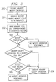
- Flash memory device 1 receives a request to perform a memory modify operation at 300. This may include interface circuitry 22 receiving input control and address signals from an external source and providing information relating to the memory modify operation to control circuit 23. Next, control circuit 23 may identify at 301 the particular sector 3 having the memory cells that are to be modified. Control circuit 23 may then control or initiate at 302 row decode circuit 7, column decode circuit 8 and sense amplifiers 9 for reading the data stored in at least some memory cells 20a and providing the data read to control circuit 23.
- control circuit 23 determines at 303 whether the sector 3 identified at 301 is modify protected, based upon the data value read from the memory cell 20a corresponding to the identified sector 3. In the event control circuit 23 determines that the identified sector 3 is modify protected, control circuit 23 does not cause the execution of the requested memory modify operation.
- control circuit 23 determines that the identified sector 3 is not modify protected and that the memory cells to be modified are not memory cells 20a (i.e., memory cells having the sector protection information)
- control circuit 23 controls at 304 memory modify circuitry 24, row decode circuit 7, column decode circuit 8 and sense amplifiers 9 for executing the requested memory modify operation.
- control circuit 23 determines at 305 whether high voltage detection circuit 25 detected a high voltage appearing on the input signal received at the input of high voltage detection circuit 25 around the time the request for the memory modify operation was received. Upon a determination that high voltage detection circuit 25 detected a high voltage signal, control circuit 23 controls at 305 memory modify circuitry 24, row decode circuit 7, column decode circuit 8 and sense amplifiers 9 for executing the requested memory modify operation at 304. However, if the high voltage detection circuit 25 did not detect a high voltage appearing on its input signal around the time the request for the memory modify operation was received, control circuit 23 does not cause the execution of the requested memory modify operation.
- flash memory device 1 may be utilized in any of a number of devices requiring nonvolatile memory.
- flash memory device 1 may be located in an electronics system 100 ( Figure 4) having a processing unit 102 that accesses data stored in flash memory device 1.
- System 100 may be, for example, a computer and/or data processing device, or a telecommunications device, such as a wireless telephone.
Landscapes
- Engineering & Computer Science (AREA)
- Computer Security & Cryptography (AREA)
- Computer Hardware Design (AREA)
- Read Only Memory (AREA)
- Semiconductor Memories (AREA)
- Non-Volatile Memory (AREA)
- Storage Device Security (AREA)
Abstract
Description
Claims (20)
- A nonvolatile memory device, comprising:an array of memory cells arranged into rows and columns and partitioned into a plurality of sectors of memory cells, memory cells in a first sector indicating at least one other sector as being modify protected;address decode circuitry for receiving an externally-generated address and selecting a row and at least one column of memory cells corresponding thereto;control circuitry, coupled to the address decode circuitry and the array of memory cells, for selectively preventing execution of a requested memory modify operation on memory cells in the at least one other sector upon an affirmative determination that at least one memory cell in the first sector indicates the at least one other sector as being modify protected.
- The nonvolatile memory device of claim 1, wherein:the nonvolatile memory device is disposed in an electronics device having a processing unit therein.
- The nonvolatile memory device of claim 1, wherein:a set of memory cells in the first sector is capable of identifying substantially any sector of memory cells as being modify protected;the nonvolatile memory device further comprises memory modify circuitry, coupled to the array and the address decode circuitry and controlled by the control circuitry, for cooperating with the address decode circuitry and the control circuitry to perform memory modify operations on memory cells in the array, memory modify operations performed on the set of memory cells utilizing the same memory modify circuitry utilized in memory modify operations performed on memory cells not in the set of memory cells.
- The nonvolatile memory device of claim 1, wherein:the nonvolatile memory device is a flash memory device.
- A method of performing a memory modify operation memory cells in a nonvolatile memory device having an array of memory cells partitioned into a plurality of sectors, the method comprising:receiving a request to perform a memory modify operation in a first sector;searching at least one memory cell in the array and determining whether the at least one memory cell identifies the first sector as being modify protected; andupon an affirmative determination that the at least one memory cell identifies the first sector as being modify protected, preventing the memory modify operation from occurring.
- The method of claim 5, further comprising:initially storing in the at least one memory cell a data value indicative of whether the at least one memory cell identifies the first sector as being modify protected.
- The method of claim 5, further comprising:initially maintaining data values in a plurality of first memory cells, including the at least one memory cell, indicating whether any of the sectors in the nonvolatile memory device is modify protected.
- The method of claim 5, further comprising:upon an affirmative determination that the at least one memory cell identifies the first sector as not being modify protected, executing the memory modify operation.
- The method of claim 5, wherein the at least one memory cell is in the first sector.
- The method of claim 5, wherein:the at least one memory cell is requested for modification by the memory modify operation; andthe method further comprises:determining whether the nonvolatile memory device received a high voltage signal associated with the request to perform the memory modify operation; andupon an affirmative determination that the nonvolatile memory device received a high voltage signal associated with the request to perform the memory modify operation and upon an affirmative determination that the at least one memory cells identifies the first sector as being not modify protected, executing the requested memory modify operation.
- The method of claim 5, wherein:the at least one memory cell is requested for modification by the memory modify operation; andthe method further comprises:determining whether the nonvolatile memory device received a high voltage signal associated with the request to perform the memory modify operation; andthe step of preventing prevents the memory modify operation from occurring upon an affirmative determination that the nonvolatile memory device received a high voltage signal associated with the request to perform the memory modify operation.
- An integrated circuit, comprising:a nonvolatile memory device, comprising:an array of nonvolatile memory cells partitioned into sectors, at least some memory cells in a first sector maintaining data indicating whether any sector is modify protected; andcontrol circuitry for selectively preventing a memory modify operation in an addressed sector from occurring based upon a data value maintained in the at least some memory cells in the first sector.
- The integrated circuit or device of claim 1 or 2, wherein:a set of memory cells in the first sector is capable of identifying any sector of memory cells as being modify protected.
- The integrated circuit or device of claim 13, wherein:a/or each memory cell in the set of memory cells is dedicated to indicating whether a distinct sector or the first sector of memory cells is modify protected.
- The integrated circuit or device of claim 1 or 2, wherein:the control circuitry selectively controls execution of a requested memory modify operation on memory cells in the at least one other sector upon an affirmative determination that at least one memory cell in the first sector indicates the at least one other sector of memory cells is modifiable.
- The integrated circuit or device of claim 12 or 14, wherein:the control circuitry selectively controls execution of requested memory read operations on the at least one memory cell in the first sector of memory cells using the same sequence of internally executed operations used in controlling execution of requested memory read operations on memory cells in the at least one other sector of memory cells.
- The integrated circuit or device of claim 1 or 12, wherein:upon reception of the requested memory modify operation on memory cells in the at least one other sector, the control circuitry controls the integrated circuit or device to:access the at least one memory cell in the first sector of memory cells to obtain at least one data value stored in the at least one memory cell; anddetermine whether the at least one data value indicates that the at least one other sector is modify protected.
- The integrated circuit or device of claim 1 or 12, wherein:a set of memory cells in the first sector is capable of identifying substantially any sector of memory cells as being modify protected; andupon reception by the integrated circuit or device of a second requested memory modify operation on memory cells in the set of memory cells, the control circuitry determines whether the integrated circuit or device received a high voltage signal, and controls execution or selectively prevents execution of the second requested memory modify operation based upon the determination.
- The integrated circuit or device of claim 18, wherein the control circuit comprises:a high voltage detection circuit for detecting the reception of a high voltage signal
- An electronics device, comprising:a nonvolatile memory device coupled to the processing unit, comprising:a processing unit; andan array of nonvolatile memory cells partitioned into sectors, at least some memory cells in a first sector maintaining data indicating whether any sector is modify protected; andcontrol circuitry for selectively preventing a memory modify operation in an addressed sector from occurring based upon a data value maintained in the at least some memory cells in the first sector.
Applications Claiming Priority (2)
| Application Number | Priority Date | Filing Date | Title |
|---|---|---|---|
| US922043 | 1986-10-17 | ||
| US09/922,043 US6490197B1 (en) | 2001-08-02 | 2001-08-02 | Sector protection circuit and method for flash memory devices |
Publications (3)
| Publication Number | Publication Date |
|---|---|
| EP1282135A2 true EP1282135A2 (en) | 2003-02-05 |
| EP1282135A3 EP1282135A3 (en) | 2004-06-30 |
| EP1282135B1 EP1282135B1 (en) | 2006-12-06 |
Family
ID=25446411
Family Applications (1)
| Application Number | Title | Priority Date | Filing Date |
|---|---|---|---|
| EP02255360A Expired - Lifetime EP1282135B1 (en) | 2001-08-02 | 2002-07-31 | Sector protection circuit and method for flash memory devices |
Country Status (4)
| Country | Link |
|---|---|
| US (1) | US6490197B1 (en) |
| EP (1) | EP1282135B1 (en) |
| JP (1) | JP4373057B2 (en) |
| DE (1) | DE60216543D1 (en) |
Cited By (1)
| Publication number | Priority date | Publication date | Assignee | Title |
|---|---|---|---|---|
| US7663915B2 (en) | 2004-02-10 | 2010-02-16 | Semiconductor Energy Laboratory Co., Ltd. | Nonvolatile memory |
Families Citing this family (12)
| Publication number | Priority date | Publication date | Assignee | Title |
|---|---|---|---|---|
| DE10108296C2 (en) * | 2001-02-21 | 2003-01-30 | Sirona Dental Systems Gmbh | Process for sensor positioning of a digital X-ray device |
| TWI259952B (en) * | 2002-01-31 | 2006-08-11 | Macronix Int Co Ltd | Data erase method of flash memory |
| ITTO20030115A1 (en) * | 2003-02-17 | 2004-08-18 | St Microelectronics Srl | SOFT-PROGRAMMING METHOD FOR A DEVICE OF |
| KR100558486B1 (en) * | 2003-07-14 | 2006-03-07 | 삼성전자주식회사 | Nonvolatile semiconductor memory device and one time programming control method thereof |
| ITRM20030354A1 (en) | 2003-07-17 | 2005-01-18 | Micron Technology Inc | CONTROL UNIT FOR MEMORY DEVICE. |
| JP2005108273A (en) * | 2003-09-26 | 2005-04-21 | Toshiba Corp | Nonvolatile semiconductor memory device |
| JP4270994B2 (en) * | 2003-09-29 | 2009-06-03 | 株式会社東芝 | Nonvolatile semiconductor memory device |
| CN101015021A (en) * | 2004-05-11 | 2007-08-08 | 斯班逊有限公司 | Semiconductor device and method of controlling the semiconductor device |
| DE602006008270D1 (en) * | 2006-03-29 | 2009-09-17 | St Microelectronics Srl | A method and apparatus for detecting possible corruption of sector protection information of a non-volatile memory stored in an on-board volatile memory array at power up |
| CN104598402B (en) * | 2014-12-30 | 2017-11-10 | 北京兆易创新科技股份有限公司 | A kind of control method of flash controller and flash controller |
| US9620216B2 (en) | 2015-02-17 | 2017-04-11 | Silicon Storage Technology, Inc. | Flash memory device configurable to provide read only memory functionality |
| KR102115638B1 (en) * | 2016-07-27 | 2020-05-27 | 매그나칩 반도체 유한회사 | Otp memory device |
Family Cites Families (6)
| Publication number | Priority date | Publication date | Assignee | Title |
|---|---|---|---|---|
| GB2251324B (en) * | 1990-12-31 | 1995-05-10 | Intel Corp | File structure for a non-volatile semiconductor memory |
| JPH0844628A (en) * | 1994-08-03 | 1996-02-16 | Hitachi Ltd | NONVOLATILE MEMORY, MEMORY CARD USING THE SAME, INFORMATION PROCESSING DEVICE, AND SOFTWARE WRITE PROTECT CONTROL METHOD FOR NONVOLATILE MEMORY |
| US5954828A (en) * | 1995-01-05 | 1999-09-21 | Macronix International Co., Ltd. | Non-volatile memory device for fault tolerant data |
| JP3489708B2 (en) * | 1996-10-23 | 2004-01-26 | シャープ株式会社 | Nonvolatile semiconductor memory device |
| US6031757A (en) * | 1996-11-22 | 2000-02-29 | Macronix International Co., Ltd. | Write protected, non-volatile memory device with user programmable sector lock capability |
| US6331950B1 (en) * | 1999-10-19 | 2001-12-18 | Fujitsu Limited | Write protect input implementation for a simultaneous operation flash memory device |
-
2001
- 2001-08-02 US US09/922,043 patent/US6490197B1/en not_active Expired - Lifetime
-
2002
- 2002-07-31 EP EP02255360A patent/EP1282135B1/en not_active Expired - Lifetime
- 2002-07-31 DE DE60216543T patent/DE60216543D1/en not_active Expired - Lifetime
- 2002-08-01 JP JP2002224398A patent/JP4373057B2/en not_active Expired - Lifetime
Cited By (1)
| Publication number | Priority date | Publication date | Assignee | Title |
|---|---|---|---|---|
| US7663915B2 (en) | 2004-02-10 | 2010-02-16 | Semiconductor Energy Laboratory Co., Ltd. | Nonvolatile memory |
Also Published As
| Publication number | Publication date |
|---|---|
| JP2003132690A (en) | 2003-05-09 |
| DE60216543D1 (en) | 2007-01-18 |
| JP4373057B2 (en) | 2009-11-25 |
| EP1282135A3 (en) | 2004-06-30 |
| EP1282135B1 (en) | 2006-12-06 |
| US6490197B1 (en) | 2002-12-03 |
Similar Documents
| Publication | Publication Date | Title |
|---|---|---|
| US6345000B1 (en) | Flash memory permitting simultaneous read/write and erase operations in a single memory array | |
| US8234440B2 (en) | Nonvolatile semiconductor memory device with advanced multi-page program operation | |
| US6552935B2 (en) | Dual bank flash memory device and method | |
| US7701762B2 (en) | NAND memory device and programming methods | |
| US9177653B2 (en) | Method and system for programming non-volatile memory cells based on programming of proximate memory cells | |
| US6594177B2 (en) | Redundancy circuit and method for replacing defective memory cells in a flash memory device | |
| KR20040029022A (en) | Non-volatile memory with block erase | |
| US6937513B1 (en) | Integrated NAND and nor-type flash memory device and method of using the same | |
| US6137729A (en) | Method for erasing memory cells in a flash memory device | |
| KR100536613B1 (en) | Nor type flash memory device being capable of reducing program time and its program method | |
| US6490197B1 (en) | Sector protection circuit and method for flash memory devices | |
| KR100781977B1 (en) | Decoder in nonvolatile memory device and decoding method thereof | |
| US7120060B2 (en) | Memory device with non-volatile reference memory cell trimming capabilities | |
| KR101405405B1 (en) | Non-volatile semiconductor memory device with dummy cells and method for adjusting threshold voltage of dummy cells | |
| CN100388391C (en) | Apparatus and method for accurate verification of or non-flash memory cells under high rank leakage | |
| JP3143161B2 (en) | Non-volatile semiconductor memory | |
| KR100645045B1 (en) | Nonvolatile Memory Device and Its Program Method | |
| US6754106B1 (en) | Reference cell with various load circuits compensating for source side loading effects in a non-volatile memory | |
| US6563732B2 (en) | Redundancy circuit and method for flash memory devices | |
| US6618286B2 (en) | Non-volatile semiconductor memory device with a memory array preventing generation of a through current path | |
| US6385091B1 (en) | Read reference scheme for non-volatile memory | |
| US6970368B1 (en) | CAM (content addressable memory) cells as part of core array in flash memory device | |
| JP3655882B2 (en) | Data storage device | |
| JP2002140893A (en) | Nonvolatile semiconductor memory device | |
| JPH10199267A (en) | Nonvolatile semiconductor memory device |
Legal Events
| Date | Code | Title | Description |
|---|---|---|---|
| PUAI | Public reference made under article 153(3) epc to a published international application that has entered the european phase |
Free format text: ORIGINAL CODE: 0009012 |
|
| AK | Designated contracting states |
Designated state(s): AT BE BG CH CY CZ DE DK EE ES FI FR GB GR IE IT LI LU MC NL PT SE SK TR |
|
| AX | Request for extension of the european patent |
Extension state: AL LT LV MK RO SI |
|
| PUAL | Search report despatched |
Free format text: ORIGINAL CODE: 0009013 |
|
| AK | Designated contracting states |
Kind code of ref document: A3 Designated state(s): AT BE BG CH CY CZ DE DK EE ES FI FR GB GR IE IT LI LU MC NL PT SE SK TR |
|
| AX | Request for extension of the european patent |
Extension state: AL LT LV MK RO SI |
|
| 17P | Request for examination filed |
Effective date: 20041220 |
|
| 17Q | First examination report despatched |
Effective date: 20050120 |
|
| AKX | Designation fees paid |
Designated state(s): DE FR GB IT |
|
| GRAP | Despatch of communication of intention to grant a patent |
Free format text: ORIGINAL CODE: EPIDOSNIGR1 |
|
| GRAS | Grant fee paid |
Free format text: ORIGINAL CODE: EPIDOSNIGR3 |
|
| GRAA | (expected) grant |
Free format text: ORIGINAL CODE: 0009210 |
|
| AK | Designated contracting states |
Kind code of ref document: B1 Designated state(s): DE FR GB IT |
|
| PG25 | Lapsed in a contracting state [announced via postgrant information from national office to epo] |
Ref country code: IT Free format text: LAPSE BECAUSE OF FAILURE TO SUBMIT A TRANSLATION OF THE DESCRIPTION OR TO PAY THE FEE WITHIN THE PRESCRIBED TIME-LIMIT;WARNING: LAPSES OF ITALIAN PATENTS WITH EFFECTIVE DATE BEFORE 2007 MAY HAVE OCCURRED AT ANY TIME BEFORE 2007. THE CORRECT EFFECTIVE DATE MAY BE DIFFERENT FROM THE ONE RECORDED. Effective date: 20061206 |
|
| REG | Reference to a national code |
Ref country code: GB Ref legal event code: FG4D |
|
| REF | Corresponds to: |
Ref document number: 60216543 Country of ref document: DE Date of ref document: 20070118 Kind code of ref document: P |
|
| PG25 | Lapsed in a contracting state [announced via postgrant information from national office to epo] |
Ref country code: DE Free format text: LAPSE BECAUSE OF FAILURE TO SUBMIT A TRANSLATION OF THE DESCRIPTION OR TO PAY THE FEE WITHIN THE PRESCRIBED TIME-LIMIT Effective date: 20070307 |
|
| ET | Fr: translation filed | ||
| PLBE | No opposition filed within time limit |
Free format text: ORIGINAL CODE: 0009261 |
|
| STAA | Information on the status of an ep patent application or granted ep patent |
Free format text: STATUS: NO OPPOSITION FILED WITHIN TIME LIMIT |
|
| 26N | No opposition filed |
Effective date: 20070907 |
|
| PGFP | Annual fee paid to national office [announced via postgrant information from national office to epo] |
Ref country code: FR Payment date: 20080718 Year of fee payment: 7 |
|
| PGFP | Annual fee paid to national office [announced via postgrant information from national office to epo] |
Ref country code: GB Payment date: 20090727 Year of fee payment: 8 |
|
| REG | Reference to a national code |
Ref country code: FR Ref legal event code: ST Effective date: 20100331 |
|
| PG25 | Lapsed in a contracting state [announced via postgrant information from national office to epo] |
Ref country code: FR Free format text: LAPSE BECAUSE OF NON-PAYMENT OF DUE FEES Effective date: 20090731 |
|
| GBPC | Gb: european patent ceased through non-payment of renewal fee |
Effective date: 20100731 |
|
| PG25 | Lapsed in a contracting state [announced via postgrant information from national office to epo] |
Ref country code: GB Free format text: LAPSE BECAUSE OF NON-PAYMENT OF DUE FEES Effective date: 20100731 |