EP1282130A2 - Sense amplifier circuit and method for nonvolatile memory devices - Google Patents
Sense amplifier circuit and method for nonvolatile memory devices Download PDFInfo
- Publication number
- EP1282130A2 EP1282130A2 EP02255359A EP02255359A EP1282130A2 EP 1282130 A2 EP1282130 A2 EP 1282130A2 EP 02255359 A EP02255359 A EP 02255359A EP 02255359 A EP02255359 A EP 02255359A EP 1282130 A2 EP1282130 A2 EP 1282130A2
- Authority
- EP
- European Patent Office
- Prior art keywords
- current
- sense
- coupled
- source
- memory
- Prior art date
- Legal status (The legal status is an assumption and is not a legal conclusion. Google has not performed a legal analysis and makes no representation as to the accuracy of the status listed.)
- Granted
Links
Images
Classifications
-
- G—PHYSICS
- G11—INFORMATION STORAGE
- G11C—STATIC STORES
- G11C7/00—Arrangements for writing information into, or reading information out from, a digital store
- G11C7/06—Sense amplifiers; Associated circuits, e.g. timing or triggering circuits
- G11C7/067—Single-ended amplifiers
-
- G—PHYSICS
- G11—INFORMATION STORAGE
- G11C—STATIC STORES
- G11C16/00—Erasable programmable read-only memories
- G11C16/02—Erasable programmable read-only memories electrically programmable
- G11C16/06—Auxiliary circuits, e.g. for writing into memory
- G11C16/26—Sensing or reading circuits; Data output circuits
- G11C16/28—Sensing or reading circuits; Data output circuits using differential sensing or reference cells, e.g. dummy cells
-
- G—PHYSICS
- G11—INFORMATION STORAGE
- G11C—STATIC STORES
- G11C7/00—Arrangements for writing information into, or reading information out from, a digital store
- G11C7/06—Sense amplifiers; Associated circuits, e.g. timing or triggering circuits
- G11C7/062—Differential amplifiers of non-latching type, e.g. comparators, long-tailed pairs
-
- G—PHYSICS
- G11—INFORMATION STORAGE
- G11C—STATIC STORES
- G11C2207/00—Indexing scheme relating to arrangements for writing information into, or reading information out from, a digital store
- G11C2207/06—Sense amplifier related aspects
- G11C2207/063—Current sense amplifiers
Definitions
- the present invention relates to sense amplification for memory devices, and particularly to circuitry for more efficiently performing sense amplification in nonvolatile memory devices.
- the first nonvolatile memories were electrically programmable read-only memories (EPROMs).
- the memory cells include a floating-gate transistor that is programmable using the hot carrier effect.
- Programming of an EPROM memory cell includes applying a potential difference between the drain and the source of the floating gate transistor in the presence of a high potential difference (of about 20 volts, this value varying according to the desired programming speed) between the control gate and the source.
- the application of the first of these potential differences generates an electrical field that gives rise to a flow of electrons in the channel. These electrons collide with atoms of the channel, causing the appearance of new free electrons. These electrons have very high energy (hence the term "hot carriers").
- EEPROMs electrically erasable programmable read only memories
- the memory cells have a floating-gate transistor whose drain is connected to the bit line by a selection transistor.
- the gate of the selection transistor is connected to the word line.
- the gate of the floating-gate transistor is controlled by a bias transistor.
- the source of the floating gate transistor is connected to a reference potential, such as ground.
- These floating-gate transistors have an oxide layer between the substrate and the floating gate that is very thin to enable the transfer of charges by tunnel effect.
- EEPROMs as compared with EPROMs lies in the fact that each memory cell is programmable and erasable independently of the other EEPROM cells.
- the tradeoff here is that a larger surface area of silicon is required and therefore a smaller scale of integration is achieved.
- Flash EPROMs A third type of memory has more recently gained popularity.
- This type of memory flash EPROMs
- Flash memory cells can be individually programmed utilizing the hot carrier effect in the same way as EPROM cells are programmed. Flash memory cells are also electrically erasable by the tunnel effect.
- the memory cells of a flash EPROM memory includes a floating-gate transistor that has an oxide layer whose thickness is greater than the oxide layer thickness of an EEPROM floating gate transistor but smaller than the oxide layer thickness of an EPROM floating gate transistor. Consequently, the flash memory cell is capable of erasure by the tunnel effect.
- Flash EPROM devices typically include at least one array of flash memory cells organized into rows and columns of flash memory cells.
- the array is typically partitioned into blocks, each of which is further divided into sectors.
- a row decoder and column decoder are used to select a single row and at least one column of memory cells based upon the value of an externally generated address applied to the flash memory device.
- Sense amplifiers are coupled to the column lines corresponding to the columns of memory cells to amplify the voltage levels on the addressed column lines corresponding to the data values stored in the addressed flash memory cells.
- the particular implementations of the array and the row and column decoders are known in the art and will not be described further for reasons of simplicity.
- a conventional sense amplifier circuit includes a differential amplifier circuit that generally senses a voltage differential between the voltage appearing on a column line connected to a reference cell and the voltage appearing on a column line connected to an addressed memory cell, and drives a sense output signal (that is coupled to the data output pins of the flash memory device) based upon the sensed voltage differential.
- the conventional sense amplifier is sized and/or powered to provide a sense output signal with a relatively high slew rate so as to reduce the time needed for the sense amplifier to sense the voltage differential and suitably drive the sense output signal.
- This extended period of sense amplifier activation combined with the sense amplifiers drawing a relatively large amount of current, disadvantageously results in the conventional flash memory device dissipating a relatively high amount of power when in use.
- This problem is compounded by the fact that more sense amplifiers are now being used in state-of-the-art burst flash devices to allow higher bandwidth (data rate) and higher frequencies for high performance systems. Consequently, the current draw and/or power dissipation of sense amplifiers for flash memory devices is no longer a trivial consideration.
- the sense amplifier includes a pair of source-coupled input transistors.
- the control or gate terminal of a first of the input transistors is driven to a voltage level based upon a current level in an addressed memory cell during a memory access operation.
- the control terminal of a second of the input transistors is driven to a voltage level based upon a current level in a reference cell during the memory access operation.
- the sense amplifier further includes a pair of load elements, with each load element being coupled between the drain terminal of a distinct one of the input transistors and a first reference voltage source, such as a ground reference.
- a current source is coupled between the source terminals of the input transistors and a second reference voltage source, such as a power supply source, and configurable to draw any of at least two non-zero current levels through the current source.
- Control circuitry within the nonvolatile memory device controls the current source so that during at least a portion of the precharge cycle of the memory access operation the current source provides a first current level, and during the subsequent sense cycle the current source provides a second current level greater than the first current level.
- the sense amplifier of the exemplary embodiment of the present invention draws a relatively small amount of current (and dissipates relatively little power) during the precharge cycle and a relatively sizeable amount of current during the sense cycle of the memory access operation.
- the sense amplifier circuit of the exemplary embodiment of the present invention performs substantially similarly as conventional sense amplifiers for memories with reduced power.
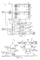
- nonvolatile memory device 1 there is disclosed a nonvolatile memory device 1 according to an exemplary embodiment of the present invention. It is understood that memory device 1 may be any type of nonvolatile memory device, such as a flash memory device. Memory device 1 will be described below as a flash memory device for reasons of simplicity.
- Flash memory device 1 includes one or more arrays or banks 2 of memory cells 20. Each array 2 of memory cells 20 may be arranged into rows and columns of memory cells 20. Each array 2 may be partitioned into blocks 3 of memory cells 20, with each block 3 being further partitioned into one or more sectors of memory cells 20 (not shown). Although flash memory device 1 is illustrated in Figure 1 as having only one array/bank 2 of memory cells 20, it is understood that flash memory device 1 may include two or more arrays 2 of memory cells 20.
- Array 2 is shown in Figure 1 as being relatively sparsely populated with memory cells 20 for reasons of clarity. It is understood that array 2 is substantially entirely populated with memory cells 20 arranged in rows and columns of memory cells 20 as described above. Although memory cells 20 are described herein as flash memory cells, it is understood that memory cells 20 may be other types of non-volatile memory cells, such as EEPROM, flash-EPROM memory cells.
- the memory cells 20 in each column may be connected to a distinct column line 5, and the memory cells 20 in each row of memory cells 20 in a block 3 may be connected to a distinct row line 6.
- Column lines 5 may be local column lines that are coupled to main column lines (not shown in Figure 2) for providing the selected local column lines to the periphery of array 2.
- main column lines not shown in Figure 2
- the use of local and main column lines in flash memories are known in the art and will not be described in greater detail for reasons of simplicity.
- Flash memory device 1 may further include row decode circuitry 7 which receives an externally generated input address or portion thereof and selects and/or activates a row of memory cells 20 based upon the input address.
- the memory cells 20 in the selected row is connected to the column lines 5.
- Row decode circuitry 7 may include logic that, for example, in response to receiving an externally generated address, drives a single row line 6 corresponding to the externally generating address to a first voltage level to activate each memory cell 20 in the row, while driving the remaining row lines 6 to another voltage level to deactivate the memory cells 20 in the remaining rows.
- Row decode circuitry 7 may be implemented with boolean logic gates as is known in the art.
- flash memory device 1 may include column decode circuitry 8 which receives an externally generated input address or portion thereof and selects one or more column lines 5 corresponding to the externally generated address.
- Column decode circuitry 8 may, for example, be implemented as multiplexing circuitry connected to each column line 5 in array 2 of memory cells 20. Column decode circuitry 8 is connected to each column line 5 of memory cells 20.
- Flash memory device 1 may include sense amplifiers 9 that sense the current flowing through the selected column lines 5 corresponding to the data stored in the addressed memory cells 20, and drive sense amplifier output signals to voltage levels that are more easily interpreted or otherwise handled by circuitry external to array 2.
- Flash memory device 1 includes a precharge circuit 16 that precharges column lines 5 during the initial portion of a memory access operation. Precharge circuit 16 is activated upon assertion of a control input signal. Upon activation, precharge circuit 16 precharges column lines 5 to a predetermined voltage level.
- Flash memory device 1 may include a data input/output (I/O) circuit 13 that generally couples addressed memory cells 20 to external I/O data pins 14 of flash memory device 1. As shown in Figure 1, data I/O circuit 13 is connected to the output of sense amplifiers 9. Flash memory device 1 may also include control circuitry 15 for receiving externally generated, input control signals and controlling the various components of flash memory device 1 to perform memory access operations. For instance, control circuit 15 may generate timing/control signals for controlling row decode circuitry 7, column decode circuitry 8, data I/O circuit 13, precharge circuit 16 and sense amplifiers 9 during a memory access operation.
- I/O data input/output
- Each memory cell 20 of flash memory device 1 is adapted to provide one of at least two distinct current levels that correspond to the data value stored in the memory cell 20.
- memory device 1 may further include a reference cell 10 which provides a predetermined current level that is between the two current levels capable of being provided by memory cell 20.
- Reference cell 10 is connected to each sense amplifier 9 in flash memory device 1. It is understood that reference cell 10 may be disposed within array 2.
- FIG. 2 is a diagram of a sense amplifier 9 according to the exemplary embodiment of the present invention.
- Sense amplifier 9 is configured as a differential amplifier circuit to sense a current differential appearing at its differential input and generate an output sense signal having a value that is based upon the sensed voltage differential.
- sense amplifier 9 includes a current-to-voltage converter circuit 9a and a voltage comparator circuit 9b connected to the output of the current-to-voltage converter circuit 9a.
- FIG. 2 shows current-to-voltage converter circuit 9a having inputs connected to a selected memory cell 20 and a reference cell 10 so as to receive a memory cell current Icell and a reference current Iref, respectively. It is understood that current-to-voltage converter circuit 9a is connected to memory cell 20 via column decode circuitry 8. Current-to-voltage converter circuit 9a generates an output Vref having a reference voltage level that is based upon reference current Iref, and an output Vcell having a voltage level that is based upon memory cell current Icell.
- Voltage comparator circuit 9b of sense amplifier 9 includes a pair of input transistors 22. Input transistors 22 are source coupled. A first input transistor 22A has a control or gate terminal coupled to signal Vref generated by current-to-voltage converter circuit 9a, and a second input transistor 22B has a control or gate terminal coupled to signal Vcell. A first load transistor 23A is coupled between the drain terminal of first input transistor 22A and the ground potential. A second load transistor 23B is coupled between the drain terminal of second input transistor 22B and ground. The gate terminals of first load transistor 23A and second load transistor 23B are connected together and to the drain terminal of first load transistor 23A so as to form a current mirror. The output of sense amplifier 9 is taken from the drain terminal of second input transistor 22B.
- Voltage comparator circuit 9b of sense amplifier 9 further includes a current source 24 coupled between the source terminals of input transistors 22 and the high reference voltage source, Vdd.
- current source 24 is configurable to source two or more nonzero current levels.
- Current source 24 includes transistor 25 having a source terminal connected to Vdd, a drain terminal coupled to the source terminals of input transistors 22 and a control or gate terminal coupled to a precharge control signal 26.
- Current source 24 further includes a transistor 27 having a source terminal connected to Vdd, a drain terminal coupled to the source terminals of input transistors 22 and a control or gate terminal coupled to a sense control signal 28.
- Transistor 27 is sized substantially larger (i.e., has a higher channel width-to-channel length ratio) than transistor 25 so as to provide or source a greater current level than the current provided by transistor 25.
- current source 24 is capable of sourcing current to input transistors 22 at a first current level during the precharge cycle of a memory access operation and at a second current level during the sense cycle of the memory access operation.
- sense amplifier 9 dissipates little power during the precharge cycle while nonetheless being able to reach the desired operating state to amplify the voltage differential appearing at the control terminals of input transistors 22.
- Sense amplifier 9 of Figure 2 shows that input transistors 22 and current source transistors 25 and 27 are p-channel field effect transistors, and load transistors 23 are n-channel field effect transistors. It is understood that, alternatively, sense amplifier 9 may be implemented with other types of transistors. Further, transistors 22, 25 and 27 may be implemented as n-channel field effect transistors and load transistors 23 may be implemented as p-channel field effect transistors in the event that the ground potential is connected to current source 24 and the high reference voltage source Vdd is connected to load transistors 23.
- control 15 includes a relatively weak driver circuit 17 having a relatively small pull-down drive transistor.
- the drive strength of driver circuit 17 is relatively weak, relative to its loading (i.e., the input loading for each sense amplifier 9 plus routing capacitance appearing on sense control line 28). In this way, driver circuit 17 relatively weakly pulls sense control line 28 from Vdd towards the ground reference, thereby providing a gradual turning on of transistors 27 and a gradual increase in sense amplifier current.
- control circuit 15 initiates the precharge cycle by activating precharge circuit 16 to precharge column lines 5 of array 2.
- precharge control signal 26 is driven to the ground potential at time T0 which activates and/or turns on transistor 25 in current source 24 of each sense amplifier 9.
- sense control signal 28 is driven to Vdd by control circuit 15.
- transistor 25 is relatively small, current source 24 sources in each sense amplifier 9 a current that is relatively small. However, the amount of current in sense amplifiers 9 is sufficient for sense amplifiers 9 to reach the desired operating point and/or state.
- the voltage of signal Vref generated by current-to-voltage converter circuit 9a may, for example, be slightly greater than voltage Vcell generated by current-to-voltage converter circuit 9a.
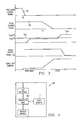
- Figure 3 illustrates the relatively low current level that is drawn in each sense amplifier 9.
- the precharge cycle is completed upon control circuit 13 deactivating precharge circuit 16.
- Each sense amplifier 9 has received at its input the current Iref generated by reference cell 10 and a current Icell corresponding to the selected memory cell 20.
- the voltage on signal Vcell generated by current-to-voltage converter circuit 9a is at a level corresponding to current Icell sunk by the selected memory cell 20, with the current level Icell being at one of two current levels based upon the data value maintained in memory cell 20.
- the signal Vref is at a voltage level corresponding to the reference current Iref sunk by the reference cell 10.
- Voltage comparator circuit 9b compares the voltage difference between voltage of signal Vcell with the voltage of signal Vref and drives the sense output signal based upon the compared voltage difference.
- control circuit 15 gradually drives at time T1 sense control signal 28 to the ground potential, which activates or turns on transistor 27.
- transistor 27 being sized to source a greater amount of current than transistor 25, current source 24 of each sense amplifier 9 provides a substantially larger amount of current than the current provided during the precharge cycle. This gives each sense amplifier 9 a substantially greater drive strength and/or ability to much more quickly drive the sense amplifier output signals to the intended voltage levels.
- Figure 3 shows the increase in current level in a sense amplifier 9 during the sense cycle of the memory read operation.
- Data I/O circuit 13 receives the output of each sense amplifier 9 and drives data output pins 14 accordingly, thereby completing the memory read operation.
- sense amplifier 9 A benefit provided by sense amplifier 9 is that, due to the fact that sense amplifier 9 operates at a reduced current during the precharge cycle of a memory access operation, sense amplifier 9 is slower to respond to spurious transitions during the precharge cycle and is therefore more immune to noise during that time.
- flash memory device 1 may be utilized in any of a number of devices requiring nonvolatile memory.
- flash memory device 1 may be located in an electronics system 100 ( Figure 4) having a processing unit 102 that accesses data stored in flash memory device 1.
- System 100 may be, for example, a computer and/or data processing device, or a telecommunications device, such as a wireless telephone.
Landscapes
- Read Only Memory (AREA)
Abstract
Description
Claims (20)
- A memory device, comprising:an array of memory cells arranged into rows and columns of memory cells, including a plurality of row lines, each row line being coupled to a distinct row of memory cells, and a plurality of column lines, each column of memory cells being coupled to a distinct column line;at least one reference memory cell;address decode circuitry coupled to receive an address and select memory cells corresponding to the received address to the column lines;precharge circuitry, coupled to each column line, for precharging the column lines to a predetermined voltage level;sense amplifiers connected to the columns lines, each sense amplifier being adapted to sense a difference between current in a selected memory cell and a current level provided by the at least one reference memory cell, and to generate a sense output signal based upon the difference, and each sense amplifier having an adjustable current level;data output circuitry connected to the sense amplifiers to receive the sense output signals from the sense amplifiers and drive external data pins based upon the voltage levels appearing on the sense output signals; andcontrol circuitry, connected to the precharge circuitry and the sense amplifiers, for selectively executing a memory access operation, the memory access operation including a precharge cycle in which the column lines are precharged by the precharge circuitry to the predetermined voltage level and the sense amplifiers are configured at a first current level, and a sense cycle following the precharge cycle in which data output circuitry drives the external pins to voltage levels based upon the sense output signals and the sense amplifiers are configured at a second current level greater than the first current level.
- The memory device of claim 1, wherein each sense amplifier comprises:a current-to-voltage converter circuit having inputs coupled to a selected memory cell and the reference memory cell and a first output signal having a voltage corresponding to current in the selected memory cell and a second output signal having a voltage corresponding to current in the reference memory cell;a pair of input transistors having control terminals coupled, during the memory access operation, to the first and second outputs of the current-to-voltage converter circuit, the sense output signal being connected to a conduction terminal of one of the input transistors;load elements coupled to the pair of input transistors; anda controllable current source controlled by the control circuitry and coupled to the pair of input transistors to provide current thereto, the controllable current source being controlled by the control circuitry to provide at least two current levels to the input transistors during the memory access operation.
- The memory device of claim 2, wherein the controllable current source comprises:a first current source controlled by the control circuitry so as to source current to the input transistors during at least a precharge cycle of the memory access operation; anda second current source parallel connected to the first current source and controlled by the control circuitry so as to source current to the input transistors during at least a sense cycle of the memory access operation.
- The memory device of claim 3, wherein:the control circuitry includes drive circuitry to gradually increase the current sourced by the second current source from a time prior to the sense cycle and extending through the sense cycle.
- The memory device of claim 2, wherein the controllable current source comprises:a first transistor having a first conduction terminal coupled to a first reference voltage source, a second conduction terminal coupled to the pair of input transistors and a control terminal coupled to a first output signal of the control circuitry to be activated during at least a precharge cycle of a memory access operation; anda second transistor having a first conduction terminal coupled to the first reference voltage source, a second conduction terminal coupled to the pair of input transistors and a control terminal coupled to a second output signal of the control circuitry to be activated during at least a sense cycle of the memory access operation.
- The memory device of claim 5, wherein:the control circuitry includes a drive circuit having a relatively weak drive transistor connected to the control terminal of the second transistor.
- The memory device of claim 5, wherein:the second transistor is substantially larger than the first transistor.
- The memory device of 5, wherein:the first and second transistors are p-channel field effect transistors;the pair of input transistors are p-channel field effect transistors; andthe load elements are n-channel field effect transistors.
- A method of performing a memory access operation on a memory device including a plurality of memory cells arranged into rows and columns, a plurality of row lines, each row line being coupled to a distinct row of memory cells, a plurality of column lines, each column of memory cells being coupled to a distinct column line, the method comprising:initially precharging the column lines to at least one predetermined voltage level;selecting a row of memory cells and connecting the memory cells in the selected row to the column lines to which the selected row of memory cells are coupled, respectively;during the precharging and connecting steps, sensing a differential between the current sunk by at least one memory cell in the selected row and a reference current;driving, at a first drive strength, at least one sense output line substantially at least a portion of the step of precharging, based upon the voltage differential;driving, at a second drive strength different from the first drive strength, the at least one sense output line substantially during the step of connecting, based upon the voltage differential; andcoupling the at least one sense output line to at least one data pin of the memory device during a portion of the step of connecting.
- The method of claim 9, further comprising:following the step of driving at the first drive strength and before the step of driving at the second drive strength, driving the at least one sense output signal at a gradually increasing drive strength, based upon the sensed voltage differential.
- The method of claim 10, wherein:the gradually increasing drive strength is between the first drive strength and the second drive strength.
- The method of claim 9, wherein:the step of driving the at least one sense output line at the first drive strength comprises driving at the first drive strength a plurality of sense output lines, each sense output line corresponding to a distinct sensed differential; andthe step of driving the at least one sense output line at the second drive strength comprises driving at the second drive strength the plurality of sense output lines.
- A sense amplifier circuit for a memory device, comprising:a pair of input transistors, each input transistor having a first source/drain terminal coupled to the first source/drain terminal of the other input transistor, a control terminal and a second source/drain terminal, an output of the sense amplifier circuit being coupled to the second source/drain terminal of one of the input transistors;a pair of load elements, each load element being coupled between the second source/drain terminal of a distinct one of the input transistors and a first reference voltage source; anda current source coupled between the first source/drain terminals of the input transistors and a second reference voltage source, and configurable to draw any of at least two non-zero current levels through the current source.
- The sense amplifier circuit of claim 13, wherein the current source comprises:a first current source having a first control input; anda second current source connected in parallel with the first current source and having a second control input.
- The sense amplifier circuit of claim 13, wherein the current source comprises:a first transistor; anda second transistor having a substantially larger width-to-length channel ratio than the width-to-length channel ratio of the first transistor and/or sized to draw a current that is substantially greater than the current capable of being drawn through the first transistor.
- The sense amplifier circuit of claim 13, wherein:the first reference voltage source is the ground reference;the second reference voltage source is a reference voltage source;the load elements are n-channel field effect transistors;the input transistors are p-channel field effect transistors; andthe current source comprises a first p-channel field effect transistor coupled between the reference voltage source and the first source/drain terminals of the input transistors, and a second field effect transistor coupled between the reference voltage source and the first source/drain terminals of the input transistors.
- The sense amplifier circuit of claim 13, wherein:the sense amplifier circuit is a sense amplifier circuit in a flash memory device.
- A memory device, comprising:an array of memory cells arranged into rows and columns of memory cells, including a plurality of row lines, each row line being coupled to a distinct row of memory cells, and a plurality of column lines, each column of memory cells being coupled to a distinct column line;at least one reference memory cell;means for precharging the column lines to at least one predetermined voltage level during a first portion of a memory access operation;means for selecting, following precharging of the column lines, a row of memory cells and connecting the memory cells in the selected row to the column lines to which the selected row of memory cells are coupled;means for sensing, during the time the column lines are precharged and during the time the column lines are connected to the memory cells in the selected row, a differential between current in at least one memory cell in the selected row and a current in the reference cell;means for driving, at a first drive strength, at least one sense output line during at least a portion of the time the column lines are precharged, based upon the differential sensed;means for driving, at a second drive strength different from the first drive strength, the at least one sense output line during a time the memory cells in the selected row are connected to the column lines, based upon the differential sensed; andmeans for connecting the at least one sense output line to data pins of the memory device.
- The memory device or method of claim 9 or 18, wherein:the second drive strength is greater than the first drive strength.
- The device or method of claim 1, 9 or 18, wherein:the memory device or cells are a flash memory device or cells.
Applications Claiming Priority (2)
| Application Number | Priority Date | Filing Date | Title |
|---|---|---|---|
| US922177 | 2001-08-02 | ||
| US09/922,177 US6535426B2 (en) | 2001-08-02 | 2001-08-02 | Sense amplifier circuit and method for nonvolatile memory devices |
Publications (3)
| Publication Number | Publication Date |
|---|---|
| EP1282130A2 true EP1282130A2 (en) | 2003-02-05 |
| EP1282130A3 EP1282130A3 (en) | 2004-05-19 |
| EP1282130B1 EP1282130B1 (en) | 2006-06-14 |
Family
ID=25446635
Family Applications (1)
| Application Number | Title | Priority Date | Filing Date |
|---|---|---|---|
| EP02255359A Expired - Lifetime EP1282130B1 (en) | 2001-08-02 | 2002-07-31 | Sense amplifier circuit and method for nonvolatile memory devices |
Country Status (4)
| Country | Link |
|---|---|
| US (2) | US6535426B2 (en) |
| EP (1) | EP1282130B1 (en) |
| JP (1) | JP2003132692A (en) |
| DE (1) | DE60212272D1 (en) |
Cited By (2)
| Publication number | Priority date | Publication date | Assignee | Title |
|---|---|---|---|---|
| WO2017139166A1 (en) * | 2016-02-10 | 2017-08-17 | Micron Technology, Inc. | Apparatuses and methods for partitioned parallel data movement |
| US10365851B2 (en) | 2015-03-12 | 2019-07-30 | Micron Technology, Inc. | Apparatuses and methods for data movement |
Families Citing this family (18)
| Publication number | Priority date | Publication date | Assignee | Title |
|---|---|---|---|---|
| JP3999900B2 (en) * | 1998-09-10 | 2007-10-31 | 株式会社東芝 | Nonvolatile semiconductor memory |
| ITRM20010001A1 (en) * | 2001-01-03 | 2002-07-03 | Micron Technology Inc | LOW VOLTAGE FLASH MEMORY DETECTION CIRCUIT. |
| US6781914B2 (en) * | 2001-08-23 | 2004-08-24 | Winbond Electronics Corp. | Flash memory having a flexible bank partition |
| US7057935B2 (en) * | 2001-08-30 | 2006-06-06 | Micron Technology, Inc. | Erase verify for non-volatile memory |
| JP3906189B2 (en) * | 2002-07-15 | 2007-04-18 | 株式会社東芝 | Nonvolatile semiconductor memory |
| US6856528B1 (en) * | 2003-07-30 | 2005-02-15 | Micron Technology, Inc. | Match line sensing amplifier for content addressable memory |
| US6982905B2 (en) * | 2003-10-09 | 2006-01-03 | Micron Technology, Inc. | Method and apparatus for reading NAND flash memory array |
| US20050222756A1 (en) * | 2004-04-05 | 2005-10-06 | Davis Scott B | Methods for displaying a route traveled by mobile users in a communication network |
| US7369450B2 (en) | 2006-05-26 | 2008-05-06 | Freescale Semiconductor, Inc. | Nonvolatile memory having latching sense amplifier and method of operation |
| US7522463B2 (en) | 2007-01-12 | 2009-04-21 | Atmel Corporation | Sense amplifier with stages to reduce capacitance mismatch in current mirror load |
| US20080247254A1 (en) * | 2007-04-05 | 2008-10-09 | Hao Thai Nguyen | Method for temperature compensating bit line during sense operations in non-volatile storage |
| US7606076B2 (en) * | 2007-04-05 | 2009-10-20 | Sandisk Corporation | Sensing in non-volatile storage using pulldown to regulated source voltage to remove system noise |
| US20090251981A1 (en) * | 2008-04-08 | 2009-10-08 | Po-Hao Huang | Memory with a fast stable sensing amplifier |
| US8867279B2 (en) * | 2012-06-21 | 2014-10-21 | Ememory Technology Inc. | Flash memory apparatus with reference word lines |
| US8947925B2 (en) | 2012-08-17 | 2015-02-03 | The University Of Connecticut | Thyristor memory cell integrated circuit |
| US9293215B2 (en) | 2014-03-18 | 2016-03-22 | Integrated Silicon Solution, Inc. | Reference current circuit with temperature coefficient correction |
| US9589601B2 (en) * | 2015-03-16 | 2017-03-07 | Arm Limited | Integrated circuit using topology configurations |
| JP6756878B1 (en) * | 2019-06-17 | 2020-09-16 | ウィンボンド エレクトロニクス コーポレーション | Semiconductor storage device |
Family Cites Families (10)
| Publication number | Priority date | Publication date | Assignee | Title |
|---|---|---|---|---|
| US4061999A (en) * | 1975-12-29 | 1977-12-06 | Mostek Corporation | Dynamic random access memory system |
| US4879682A (en) * | 1988-09-15 | 1989-11-07 | Motorola, Inc. | Sense amplifier precharge control |
| IT1246241B (en) * | 1990-02-23 | 1994-11-17 | Sgs Thomson Microelectronics | CIRCUIT FOR READING THE INFORMATION CONTAINED IN NON-VOLATILE MEMORY CELLS |
| KR940003409B1 (en) * | 1991-07-31 | 1994-04-21 | 삼성전자 주식회사 | Sense Amplifier Control Circuit of Semiconductor Memory Device |
| EP0805454A1 (en) * | 1996-04-30 | 1997-11-05 | STMicroelectronics S.r.l. | Sensing circuit for reading and verifying the content of a memory cell |
| DE69631123D1 (en) * | 1996-06-18 | 2004-01-29 | St Microelectronics Srl | Method and circuit for reading non-volatile memory cells with a low supply voltage |
| US5805500A (en) * | 1997-06-18 | 1998-09-08 | Sgs-Thomson Microelectronics S.R.L. | Circuit and method for generating a read reference signal for nonvolatile memory cells |
| FR2778012B1 (en) * | 1998-04-28 | 2001-09-28 | Sgs Thomson Microelectronics | DEVICE AND METHOD FOR READING EEPROM MEMORY CELLS |
| JP3116921B2 (en) * | 1998-09-22 | 2000-12-11 | 日本電気株式会社 | Semiconductor storage device |
| KR100296911B1 (en) * | 1998-10-28 | 2001-08-07 | 박종섭 | Current direction sense amplifier |
-
2001
- 2001-08-02 US US09/922,177 patent/US6535426B2/en not_active Expired - Lifetime
-
2002
- 2002-07-31 EP EP02255359A patent/EP1282130B1/en not_active Expired - Lifetime
- 2002-07-31 DE DE60212272T patent/DE60212272D1/en not_active Expired - Fee Related
- 2002-08-02 JP JP2002225477A patent/JP2003132692A/en active Pending
-
2003
- 2003-01-15 US US10/345,474 patent/US6665213B1/en not_active Expired - Lifetime
Cited By (10)
| Publication number | Priority date | Publication date | Assignee | Title |
|---|---|---|---|---|
| US10365851B2 (en) | 2015-03-12 | 2019-07-30 | Micron Technology, Inc. | Apparatuses and methods for data movement |
| US10936235B2 (en) | 2015-03-12 | 2021-03-02 | Micron Technology, Inc. | Apparatuses and methods for data movement |
| US11614877B2 (en) | 2015-03-12 | 2023-03-28 | Micron Technology, Inc. | Apparatuses and methods for data movement |
| WO2017139166A1 (en) * | 2016-02-10 | 2017-08-17 | Micron Technology, Inc. | Apparatuses and methods for partitioned parallel data movement |
| US10048888B2 (en) | 2016-02-10 | 2018-08-14 | Micron Technology, Inc. | Apparatuses and methods for partitioned parallel data movement |
| CN108604169A (en) * | 2016-02-10 | 2018-09-28 | 美光科技公司 | Device and method for the movement of segmented parallel data |
| US10324654B2 (en) | 2016-02-10 | 2019-06-18 | Micron Technology, Inc. | Apparatuses and methods for partitioned parallel data movement |
| CN108604169B (en) * | 2016-02-10 | 2020-04-21 | 美光科技公司 | Apparatus and method for partitioned parallel data movement |
| US10915263B2 (en) | 2016-02-10 | 2021-02-09 | Micron Technology, Inc. | Apparatuses and methods for partitioned parallel data movement |
| US11513713B2 (en) | 2016-02-10 | 2022-11-29 | Micron Technology, Inc. | Apparatuses and methods for partitioned parallel data movement |
Also Published As
| Publication number | Publication date |
|---|---|
| JP2003132692A (en) | 2003-05-09 |
| US6665213B1 (en) | 2003-12-16 |
| US6535426B2 (en) | 2003-03-18 |
| EP1282130B1 (en) | 2006-06-14 |
| DE60212272D1 (en) | 2006-07-27 |
| EP1282130A3 (en) | 2004-05-19 |
| US20030026128A1 (en) | 2003-02-06 |
Similar Documents
| Publication | Publication Date | Title |
|---|---|---|
| EP1282130B1 (en) | Sense amplifier circuit and method for nonvolatile memory devices | |
| US7542339B2 (en) | Clock synchronized non-volatile memory device | |
| KR100271858B1 (en) | Semiconductor integrated circuit device | |
| US5414658A (en) | Electrically erasable programmable read-only memory array | |
| US8238158B2 (en) | Programming of memory cells in a nonvolatile memory using an active transition control | |
| EP1282131B1 (en) | Reference generator circuit and method for nonvolatile memory devices | |
| US9355734B2 (en) | Sensing circuits for use in low power nanometer flash memory devices | |
| EP4243081A2 (en) | Improved flash memory cell associated decoders | |
| JP2002197876A (en) | Writing method for nonvolatile storage device | |
| US6424571B1 (en) | Sense amplifier with data line precharge through a self-bias circuit and a precharge circuit | |
| KR100784473B1 (en) | Word Line Decoding Structure in Flash Memory | |
| EP0842514B1 (en) | Flash memory system having reduced disturb and method | |
| US7813198B2 (en) | System and method for reading memory | |
| US5784319A (en) | Method for erasing an electrically programmable and erasable non-volatile memory cell | |
| JP2002533867A (en) | Zero static power memory decoder | |
| US6038173A (en) | Memory read circuit with dynamically controlled precharging device | |
| US6195295B1 (en) | Segmented column memory device voltage steering technique | |
| KR100378324B1 (en) | Segmented column memory device voltage steering technique |
Legal Events
| Date | Code | Title | Description |
|---|---|---|---|
| PUAI | Public reference made under article 153(3) epc to a published international application that has entered the european phase |
Free format text: ORIGINAL CODE: 0009012 |
|
| AK | Designated contracting states |
Designated state(s): AT BE BG CH CY CZ DE DK EE ES FI FR GB GR IE IT LI LU MC NL PT SE SK TR |
|
| AX | Request for extension of the european patent |
Extension state: AL LT LV MK RO SI |
|
| PUAL | Search report despatched |
Free format text: ORIGINAL CODE: 0009013 |
|
| AK | Designated contracting states |
Kind code of ref document: A3 Designated state(s): AT BE BG CH CY CZ DE DK EE ES FI FR GB GR IE IT LI LU MC NL PT SE SK TR |
|
| AX | Request for extension of the european patent |
Extension state: AL LT LV MK RO SI |
|
| RIC1 | Information provided on ipc code assigned before grant |
Ipc: 7G 11C 16/28 B Ipc: 7G 11C 7/06 A |
|
| 17P | Request for examination filed |
Effective date: 20041110 |
|
| 17Q | First examination report despatched |
Effective date: 20041208 |
|
| AKX | Designation fees paid |
Designated state(s): DE FR GB IT |
|
| GRAP | Despatch of communication of intention to grant a patent |
Free format text: ORIGINAL CODE: EPIDOSNIGR1 |
|
| GRAS | Grant fee paid |
Free format text: ORIGINAL CODE: EPIDOSNIGR3 |
|
| GRAA | (expected) grant |
Free format text: ORIGINAL CODE: 0009210 |
|
| AK | Designated contracting states |
Kind code of ref document: B1 Designated state(s): DE FR GB IT |
|
| PG25 | Lapsed in a contracting state [announced via postgrant information from national office to epo] |
Ref country code: IT Free format text: LAPSE BECAUSE OF FAILURE TO SUBMIT A TRANSLATION OF THE DESCRIPTION OR TO PAY THE FEE WITHIN THE PRESCRIBED TIME-LIMIT;WARNING: LAPSES OF ITALIAN PATENTS WITH EFFECTIVE DATE BEFORE 2007 MAY HAVE OCCURRED AT ANY TIME BEFORE 2007. THE CORRECT EFFECTIVE DATE MAY BE DIFFERENT FROM THE ONE RECORDED. Effective date: 20060614 |
|
| REG | Reference to a national code |
Ref country code: GB Ref legal event code: FG4D |
|
| REF | Corresponds to: |
Ref document number: 60212272 Country of ref document: DE Date of ref document: 20060727 Kind code of ref document: P |
|
| ET | Fr: translation filed | ||
| PG25 | Lapsed in a contracting state [announced via postgrant information from national office to epo] |
Ref country code: DE Free format text: LAPSE BECAUSE OF NON-PAYMENT OF DUE FEES Effective date: 20070201 |
|
| PLBE | No opposition filed within time limit |
Free format text: ORIGINAL CODE: 0009261 |
|
| STAA | Information on the status of an ep patent application or granted ep patent |
Free format text: STATUS: NO OPPOSITION FILED WITHIN TIME LIMIT |
|
| 26N | No opposition filed |
Effective date: 20070315 |
|
| PGFP | Annual fee paid to national office [announced via postgrant information from national office to epo] |
Ref country code: GB Payment date: 20070725 Year of fee payment: 6 |
|
| PGFP | Annual fee paid to national office [announced via postgrant information from national office to epo] |
Ref country code: FR Payment date: 20070710 Year of fee payment: 6 |
|
| GBPC | Gb: european patent ceased through non-payment of renewal fee |
Effective date: 20080731 |
|
| REG | Reference to a national code |
Ref country code: FR Ref legal event code: ST Effective date: 20090331 |
|
| PG25 | Lapsed in a contracting state [announced via postgrant information from national office to epo] |
Ref country code: GB Free format text: LAPSE BECAUSE OF NON-PAYMENT OF DUE FEES Effective date: 20080731 |
|
| PG25 | Lapsed in a contracting state [announced via postgrant information from national office to epo] |
Ref country code: FR Free format text: LAPSE BECAUSE OF NON-PAYMENT OF DUE FEES Effective date: 20080731 |