EP1282117A2 - Adaptive writing method and circuit for a high-density optical recording apparatus - Google Patents
Adaptive writing method and circuit for a high-density optical recording apparatus Download PDFInfo
- Publication number
- EP1282117A2 EP1282117A2 EP02079350A EP02079350A EP1282117A2 EP 1282117 A2 EP1282117 A2 EP 1282117A2 EP 02079350 A EP02079350 A EP 02079350A EP 02079350 A EP02079350 A EP 02079350A EP 1282117 A2 EP1282117 A2 EP 1282117A2
- Authority
- EP
- European Patent Office
- Prior art keywords
- pulse
- magnitude
- write
- accordance
- adaptive
- Prior art date
- Legal status (The legal status is an assumption and is not a legal conclusion. Google has not performed a legal analysis and makes no representation as to the accuracy of the status listed.)
- Granted
Links
Images


Classifications
-
- G—PHYSICS
- G11—INFORMATION STORAGE
- G11B—INFORMATION STORAGE BASED ON RELATIVE MOVEMENT BETWEEN RECORD CARRIER AND TRANSDUCER
- G11B7/00—Recording or reproducing by optical means, e.g. recording using a thermal beam of optical radiation by modifying optical properties or the physical structure, reproducing using an optical beam at lower power by sensing optical properties; Record carriers therefor
- G11B7/004—Recording, reproducing or erasing methods; Read, write or erase circuits therefor
- G11B7/006—Overwriting
- G11B7/0062—Overwriting strategies, e.g. recording pulse sequences with erasing level used for phase-change media
-
- G—PHYSICS
- G11—INFORMATION STORAGE
- G11B—INFORMATION STORAGE BASED ON RELATIVE MOVEMENT BETWEEN RECORD CARRIER AND TRANSDUCER
- G11B20/00—Signal processing not specific to the method of recording or reproducing; Circuits therefor
- G11B20/10—Digital recording or reproducing
- G11B20/10009—Improvement or modification of read or write signals
-
- G—PHYSICS
- G11—INFORMATION STORAGE
- G11B—INFORMATION STORAGE BASED ON RELATIVE MOVEMENT BETWEEN RECORD CARRIER AND TRANSDUCER
- G11B20/00—Signal processing not specific to the method of recording or reproducing; Circuits therefor
- G11B20/10—Digital recording or reproducing
- G11B20/14—Digital recording or reproducing using self-clocking codes
- G11B20/1403—Digital recording or reproducing using self-clocking codes characterised by the use of two levels
-
- G—PHYSICS
- G11—INFORMATION STORAGE
- G11B—INFORMATION STORAGE BASED ON RELATIVE MOVEMENT BETWEEN RECORD CARRIER AND TRANSDUCER
- G11B7/00—Recording or reproducing by optical means, e.g. recording using a thermal beam of optical radiation by modifying optical properties or the physical structure, reproducing using an optical beam at lower power by sensing optical properties; Record carriers therefor
- G11B7/004—Recording, reproducing or erasing methods; Read, write or erase circuits therefor
- G11B7/0045—Recording
-
- G—PHYSICS
- G11—INFORMATION STORAGE
- G11B—INFORMATION STORAGE BASED ON RELATIVE MOVEMENT BETWEEN RECORD CARRIER AND TRANSDUCER
- G11B7/00—Recording or reproducing by optical means, e.g. recording using a thermal beam of optical radiation by modifying optical properties or the physical structure, reproducing using an optical beam at lower power by sensing optical properties; Record carriers therefor
- G11B7/007—Arrangement of the information on the record carrier, e.g. form of tracks, actual track shape, e.g. wobbled, or cross-section, e.g. v-shaped; Sequential information structures, e.g. sectoring or header formats within a track
- G11B7/00718—Groove and land recording, i.e. user data recorded both in the grooves and on the lands
-
- G—PHYSICS
- G11—INFORMATION STORAGE
- G11B—INFORMATION STORAGE BASED ON RELATIVE MOVEMENT BETWEEN RECORD CARRIER AND TRANSDUCER
- G11B7/00—Recording or reproducing by optical means, e.g. recording using a thermal beam of optical radiation by modifying optical properties or the physical structure, reproducing using an optical beam at lower power by sensing optical properties; Record carriers therefor
- G11B7/12—Heads, e.g. forming of the optical beam spot or modulation of the optical beam
- G11B7/125—Optical beam sources therefor, e.g. laser control circuitry specially adapted for optical storage devices; Modulators, e.g. means for controlling the size or intensity of optical spots or optical traces
- G11B7/126—Circuits, methods or arrangements for laser control or stabilisation
- G11B7/1263—Power control during transducing, e.g. by monitoring
Definitions
- the present invention relates to an adaptive writing method for a high-density optical recording apparatus and a circuit thereof, and more particularly, to an adaptive writing method for optimizing light power of a light source, e.g., a laser diode, to be suitable to characteristics of a recording apparatus, and a circuit thereof.
- a light source e.g., a laser diode
- optical recording systems employing high-capacity recording media, such as a magnetic optical disc drive (MODD) or a digital versatile disc random access memory (DVD-RAM) drive, have been widely used.
- MODD magnetic optical disc drive
- DVD-RAM digital versatile disc random access memory
- a write pulse is formed as specified in the DVD-RAM format shown in Figure 1B, with respect to input NRZI (Non-Return to Zero Inversion) data having marks of 3T, 5T and 11T (T being the channel clock duration), as shown in Figure 1A.
- the NRZI data is divided into mark and space. The spaces are in an erase power level for overwriting.
- the waveform of a write pulse for marks equal to or longer than 3T mark, that is, 3T, 4T,...11T and 14T is comprised of a first pulse, a last pulse and a multi-pulse train.
- only the number of pulses in the multi-pulse train is varied depending on the magnitude of a mark.
- the waveform of the write pulse comprises a combination of read power (Figure 1C), peak power or write power (Figure 1D) and bias power or erase power (Figure 1E).
- Figure 1C read power
- Figure 1D peak power or write power
- Figure 1E bias power or erase power
- the respective power signals shown in Figures 1C, 1D and 1E are all low-active signals.
- the waveform of the write pulse is the same as that in accordance with the first generation 2.6 GB DVD-RAM standard.
- the waveform of the write pulse is comprised of a first pulse, a multi-pulse train and a last pulse.
- the rising edge of the first pulse or the falling edge of the last pulse can be read from a lead-in area to be used, adaptive writing is not possible since the write pulse is fixed to be constant.
- an apparatus for use in an adaptive writing circuit for writing input data on an optical recording medium using a write pulse for a light source and whose waveform comprises a first pulse, a last pulse and a multi-pulse train comprising: a discriminator to discriminate a magnitude of the present mark of the input data and magnitudes of the leading and/or trailing spaces of the present mark; a generator to control the waveform of the write pulse in accordance with the magnitude of the present mark of the input data and the magnitudes of the leading and/or trailing spaces to generate an adaptive write pulse; and a driver to drive the light source by converting the adaptive write pulse into a current signal in accordance with driving power levels for respective channels for the adaptive write pulse.
- the generator includes: a write waveform controller to generate pulse width data to vary a width of the first pulse in accordance with the magnitude of the leading space and the magnitude of the present mark and to vary a width of the last pulse in accordance with the magnitude of the present mark and the magnitude of the trailing space; and a write pulse generator to generate the adaptive write pulse in accordance with the pulse width data.
- the write waveform controller comprises a memory in which the pulse width data of the first and/or last pulses of the write pulse waveform are stored, by grouping the magnitude of the present mark and the magnitudes of the leading and/or trailing spaces, into a short pulse group, a middle pulse group or along pulse group.
- the apparatus may further comprise a microcomputer to initialize the write waveform controller and control the pulse width data stored in the memory to be updated in accordance with write conditions.
- the memory preferably stores the pulse width data of the first and/or last pulses of a write pulse waveform depending on whether the input data is in a land track or a groove track.
- the memory may store the pulse width data of the first and/or last pulses of the write pulse waveform for respective zones on the optical recording medium.
- light power for a predetermined one of channels of the adaptive write pulse is applied during a period corresponding to a varied width of the first pulse and during a period corresponding to a varied width of the last pulse.
- the light power for the predetermined channel is a read power or a write power.
- the generator generates pulse width data by varying a rising edge of the first pulse in accordance with the magnitude of the leading space and the magnitude of the present mark.
- the generator may generate pulse width data by varying a falling edge of the last pulse in accordance with the magnitude of the trailing space and the magnitude of the present mark.
- an apparatus for use in an adaptive writing circuit for writing input data to an optical recording medium using a write pulse for a light source and whose waveform includes a first pulse, a last pulse and a multi-pulse train comprising: a generator to generate an adaptive write pulse by varying a rising edge of the first pulse in accordance with a magnitude of a leading space and a magnitude of the present mark, and varying a falling edge of the last pulse in accordance with the magnitude of a trailing space and the magnitude of the present mark; and a driver to drive the light source according to the adaptive write pulse.
- an apparatus for use in an adaptive write pulse generating circuit the adaptive write pulse being used for writing input data to an optical recording medium
- the apparatus comprising: a discriminator to which a write pulse is input, the write pulse including a first pulse, a last pulse and a multi-pulse train; a generator generating the adaptive write pulse by varying a rising edge of the first pulse in accordance with a magnitude of a leading space and a magnitude of a present mark, and varying a falling edge of the last pulse in accordance with a magnitude of a trailing space and the magnitude of the present mark; and an driver to output the generated adaptive write pulse.
- a method for writing input data on an optical recording medium by a write pulse whose waveform is comprised of a first pulse, a last pulse and a multi-pulse train the adaptive writing method including the steps of controlling the waveform of the write pulse in accordance with the magnitude of the present mark of the input data and the magnitudes of the leading and/or trailing spaces to generate an adaptive write pulse, and writing the input data by the adaptive write pulse on the optical recording medium.
- the method includes the step of generating an adaptive write pulse in which the rising edge of the first pulse is varied in accordance with the magnitude of the leading space and the magnitude of the present mark.
- the falling edge of the last pulse is varied in accordance with the magnitude of the present mark and the magnitude of the trailing space.
- the rising edge of the first pulse is varied in accordance with the magnitude of the leading space and the magnitude of the present mark
- the falling edge of the last pulse is varied in accordance with the magnitude of the present mark and the magnitude of the trailing space.
- the method includes the step of generating an adaptive write pulse in which the rising edge of the first pulse is shifted back and forth in accordance with the magnitude of the leading space and the magnitude of the present mark, and the falling edge of the last pulse is shifted back and forth in accordance with the magnitude of the present mark and the magnitude of the trailing space.
- the light power for a predetermined channel is applied during the period corresponding to the shift of the rising edge of the first pulse and during the period corresponding to the shift of the falling edge of the last pulse.
- the light power for a predetermined channel is either read power or write power.
- the method comprises the step of correcting the waveform of the adaptive write pulse in accordance with a land/groove signal indicating whether the input data is data of a land track or data of a groove track.
- an apparatus for writing input data on an optical recording medium by a write pulse whose waveform is comprised of a first pulse, a last pulse and a multi-pulse train the adaptive writing circuit including a discriminator for discriminating the magnitude of the present mark of the input data and the magnitudes of the leading and/or trailing spaces, a generator for controlling the waveform of the write pulse in accordance with the magnitude of the present mark of the input data and the magnitudes of the leading and/or trailing spaces to generate an adaptive write pulse, and a driver for driving the light source by converting the adaptive write pulse into a current signal in accordance with driving power levels for the respective channels.
- the generator includes a write waveform controller for generating pulse width data for varying the width of the first pulse in accordance with the magnitude of the leading space and the magnitude of the present mark and varying the width of the last pulse in accordance with the magnitude of the present mark and the magnitude of the leading space, and a write pulse generator for generating an adaptive write pulse in accordance with the pulse width data.
- a write waveform controller for generating pulse width data for varying the width of the first pulse in accordance with the magnitude of the leading space and the magnitude of the present mark and varying the width of the last pulse in accordance with the magnitude of the present mark and the magnitude of the leading space
- a write pulse generator for generating an adaptive write pulse in accordance with the pulse width data.
- the write waveform controller comprises a memory in which width data of the first and/or last pulses of a write pulse waveform are stored, by grouping the magnitude of the present mark and the magnitudes of the leading and/or trailing spaces, into a short pulse group, a middle pulse group and a long pulse group.
- the apparatus comprises a microcomputer for initializing the write waveform controller and controlling the pulse width data stored in the memory to be updated in accordance with write conditions.
- the memory stores width data of the first and/or last pulses of a write pulse waveform depending on whether the input data is in a land track or a groove track.
- the memory stores width data of the first and/or last pulses of a write pulse waveform for the respective zones on a recording medium.
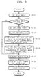
- a preferred adaptive writing circuit includes a data discriminator 102, a write waveform controller 104, a microcomputer 106, a write pulse generator 108 and a current driver 110.
- the data discriminator 102 discriminates input NRZI data.
- the write waveform controller 104 corrects the waveform of a write pulse in accordance with the discrimination result of the data discriminator 102 and a land/groove signal.
- the microcomputer 106 initializes the write waveform controller 104 or controls the data stored in the write waveform controller 104 to be updated in accordance with write conditions.
- the write pulse generator 108 generates an adaptive write pulse in accordance with the output of the write waveform controller 104.
- the current driver 110 converts the adaptive write pulse generated from the write pulse generator 108 into a current signal in accordance with the light power levels of the respective channels to drive a light source.
- the data discriminator 102 discriminates the magnitude of a mark corresponding to the present write pulse (to be referred to as a present mark), the magnitude of the front-part space corresponding to the first pulse of the present mark (to be referred to as a leading space, hereinafter) and the magnitude of the rear-part space corresponding to the last pulse of the present mark (to be referred to as a trailing space) from input NRZI data, and applies the magnitudes of the leading and trailing spaces and the magnitude of the present mark to the write waveform controller 104.
- the magnitudes of the leading and trailing spaces and the magnitude of the present mark may range from 3T to 14T. There can be more than 1,000 possible combinations. Thus, circuits or memories for obtaining the amounts of shift in rising edges of the first pulses and falling edges of the last pulses are necessary with respect to all cases, which complicates the system and hardware. Therefore, in the present invention, the magnitudes of the present mark and the leading and trailing spaces of input NRZI data are grouped into a short pulse group, a middle pulse group and a long pulse group and the grouped magnitudes of the present mark and the leading and trailing spaces are used.
- the write waveform controller 104 shifts the rising edge of the first pulse back and forth in accordance with the magnitudes of the leading space and the present mark, supplied from the data discriminator 102, or shifts the falling edge of the last pulse back and forth in accordance with the magnitudes of the present mark and the trailing space, to thus form a write waveform having an optimal light power.
- the multi-pulse train of a mark takes the same shape as shown in Figure 3B, that is, 0.5 T.
- the write waveform controller 104 can correct the rising edge of the first pulse of the present mark and the falling edge of the last pulse of the present mark into different values in accordance with externally applied land/groove signals (LAND/GROOVE) indicating whether the input NRZI data is in a land track or a groove track.
- LAND/GROOVE externally applied land/groove signals
- This is for forming a write waveform in consideration of different optimal light powers depending on the land and groove. A difference of 1-2 mW in the optimal light powers between the land and the groove, and may be specifically set or managed by the specifications.
- the write waveform controller 104 suitably comprises a memory to store data corresponding to a shift value of the rising edge of the first pulse and a shift value of the falling edge of the last pulse in accordance with the magnitude of the present mark of input NRZI data and the magnitudes of the leading and trailing spaces thereof.
- the waveform controller 104 suitably comprises a logic circuit.
- the widths of the first pulse and the last pulse are determined as channel clocks (T) plus and minus a data value (shift value) stored in the memory.
- shift values of the first and last pulses of the mark for each of a land and a groove may be stored.
- a table in which the shift value of the rising edge of the first pulse is stored and a table in which the shift value of the falling edge of the last pulse is stored may be incorporated.
- two separate tables may be prepared.
- a microcomputer 106 initializes the write waveform controller 104 or controls the shift values of the first and/or last pulse(s) to be updated in accordance with recording conditions.
- the light power can vary or the shift values of the first and last pulses can be reset.
- the pulse width data for controlling the waveform of the write pulse is provided to the write pulse generator 108.
- the write pulse generator 108 generates an adaptive write pulse, as shown in Figure 3F, in accordance with the pulse width data for controlling the waveform of the write pulse supplied from the write waveform controller 104 and supplies control signals shown in Figures 3C, 3D and 3E, for controlling the current flow for the respective channels (i.e., read, peak and bias channels) for the adaptive write pulse, to the current driver 110.
- the current driver 110 converts the driving level of the light power of the respective channels (i.e., read, peak and bias channels) into current for a control time corresponding to the control signal for controlling the current flow of the respective channels to allow the current to flow through the laser diode so that an appropriate amount of heat is applied to the recording medium by continuous ON-OFF operations of the laser diode or a change in the amounts of light.
- a record domain as shown in Figure 3G is formed on the recording medium.
- Figure 3A shows input NRZI data, which is divided into mark and space.
- Figure 3B shows a basic write waveform, in which the rising edge of the first pulse of the write pulse lags behind by 0.5T, compared to the rising edge of the present mark.
- Figure 3C shows the waveform of a read power of the adaptive write pulse
- Figure 3D shows the waveform of a peak power of the adaptive write pulse
- Figure 3E shows the waveform of a bias power of the adaptive write pulse.
- Figure 3F shows the waveform of the adaptive write pulse proposed in the present invention.
- the rising edge of the first pulse of the write waveform of the adaptive write pulse may be shifted back and forth in accordance with a combination of the magnitude of the leading space and the magnitude of the present mark.
- An arbitrary power (here, a read power or a write power) is applied during the period corresponding to the shift.
- the falling edge of the last pulse of the adaptive write pulse may be shifted back and forth in accordance with a combination of the magnitude of the present mark and the magnitude of the trailing space.
- an arbitrary power (here, a read power or a write power) is applied during the period corresponding to the shift.
- the falling edge of the last pulse may be shifted back and forth in accordance with the magnitude of the present mark, regardless of the magnitude of the trailing space of the present mark.
- the edge of any one pulse may be shifted. Also, in view of the direction of shift, shifting may be performed back and forth, only forward or only backward.
- Figure 4 illustrates grouping of input NRZI data, showing two examples of grouping.
- first example if a low grouping pointer is 3 and a high grouping pointer is 12, then the mark of a short pulse group is 3T, the marks of a middle pulse group are from 4T to 11T and the mark of a long pulse group is 14T.
- second example if a low grouping pointer is 4 and a high grouping pointer is 11, then the marks of a short pulse group are 3T and 4T, the marks of a middle pulse group are from 5T to 10T and the marks of a long pulse group are 11T and 14T.
- grouping can be performed differently for the respective zones.
- Figure 5 illustrates a number of cases depending on combinations of leading and trailing spaces and present marks, in the case of classifying input NRZI data into three groups, as shown in Figure 4, using grouping pointers.
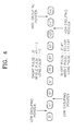
- Figure 6 illustrates a table showing shift values of rising edges of the first pulse depending on the magnitude of the leading space and the magnitude of the present mark.
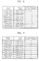
- Figure 7 illustrates a table showing shift values of falling edges of the last pulse depending on the magnitude of the present mark and the magnitude of the trailing space.
- FIG 8 is a flow chart illustrating an embodiment of an adaptive writing method of the present invention.
- a write mode is set (step S101). If the write mode is set, it is determined whether it is an adaptive writing mode or not (step S102). If it is determined in step S102 that the write mode is an adaptive write mode, a grouping pointer is set (step S103). Then, a grouping table depending on the set grouping pointer is selected (step S104).
- the selected grouping table may be a table reflecting land/groove as well as the grouping pointer. Also, the selected grouping table may be a table reflecting zones of the recording medium.
- Shift values of the rising edge of the first pulse are read from the table shown in Figure 7 in accordance with a combination of the present mark and the trailing space (step S106).
- the adaptive write pulse in which the first pulse and the last pulse are controlled in accordance with the read shift value is generated (step S107). Then, the light powers of the respective channels for the generated adaptive write pulse, i.e., read, peak and bias powers, are controlled to drive a laser diode (step S108) to then perform a write operation on a disc (step S109). If the write mode is not an adaptive write mode, a general write pulse is generated in step S107.
- Figure 9 is a graph for comparing jitter generated by the adaptive writing method according to the present invention and the conventional writing method. It is understood that, assuming that the peak light is 9.5 mW, the bottom power of a multi-pulse train is 1.2 mW, the cooling power is 1.2 mW and the bias power is 5.2 mW, there is less jitter generated when writing the adaptive write pulse according to the present invention than when generated writing the fixed write pulse according to the conventional writing method.
- the initialization conditions are a speed of 4.2 m/s, an erase power of 7.2 mW and 100 write operations.
- the rising edge of the first pulse is adaptively shifted in accordance with the magnitude of the leading space and the magnitude of the present mark of input NRZI data to thus control the waveform of the write pulse
- the falling edge of the last pulse is adaptively shifted in accordance with the magnitude of the present mark and the magnitude of the trailing space of input NRZI data to thus control the waveform of the write pulse, thereby minimizing jitter.
- the waveform of the write pulse may be optimized in accordance with land/groove signals. Further, grouping may be performed differently for the respective zones, using grouping pointers.
- the adaptive writing method described above can be adopted to most high-density optical recording apparatus using an adaptive writing pulse.
- the widths of the first and/or last pulses of a write pulse waveform are varied in accordance with the magnitude of the present mark of input NRZI data and the magnitude of the leading or trailing space, thereby minimizing jitter to enhance system reliability and performance. Also, the width of a write pulse is controlled by grouping the magnitude of the present mark and the magnitude of the leading or trailing spaces, thereby reducing the size of a hardware.
Abstract
Description
- The present invention relates to an adaptive writing method for a high-density optical recording apparatus and a circuit thereof, and more particularly, to an adaptive writing method for optimizing light power of a light source, e.g., a laser diode, to be suitable to characteristics of a recording apparatus, and a circuit thereof.
- With the multi-media era requiring high-capacity recording media, optical recording systems employing high-capacity recording media, such as a magnetic optical disc drive (MODD) or a digital versatile disc random access memory (DVD-RAM) drive, have been widely used.
- As the recoding density increases, such optical recording systems require optimal and high-precision states. In general, with an increase in recording density, temporal fluctuation (to be referred to as jitter, hereinafter) in a data domain increases. Thus, in order to attain high-density recording, it is very important to minimize the jitter.
- Conventionally, a write pulse is formed as specified in the DVD-RAM format shown in Figure 1B, with respect to input NRZI (Non-Return to Zero Inversion) data having marks of 3T, 5T and 11T (T being the channel clock duration), as shown in Figure 1A. Here, the NRZI data is divided into mark and space. The spaces are in an erase power level for overwriting. The waveform of a write pulse for marks equal to or longer than 3T mark, that is, 3T, 4T,...11T and 14T is comprised of a first pulse, a last pulse and a multi-pulse train. Here, only the number of pulses in the multi-pulse train is varied depending on the magnitude of a mark.
- In other words, the waveform of the write pulse comprises a combination of read power (Figure 1C), peak power or write power (Figure 1D) and bias power or erase power (Figure 1E). Here, the respective power signals shown in Figures 1C, 1D and 1E are all low-active signals.
- The waveform of the write pulse is the same as that in accordance with the first generation 2.6 GB DVD-RAM standard. In other words, in accordance with the 2.6 GB DVD-RAM standard, the waveform of the write pulse is comprised of a first pulse, a multi-pulse train and a last pulse. Although the rising edge of the first pulse or the falling edge of the last pulse can be read from a lead-in area to be used, adaptive writing is not possible since the write pulse is fixed to be constant.
- Therefore, when a write operation is performed by forming such a write pulse as shown in Figure 1B, severe thermal interference may occur back and forth with respect to a mark in accordance with input NRZI data. In other words, when a mark is long and a space is short or vice versa, jitter is most severe. This is a major cause of lowered system performance. Also, this does not make it possible for the system to be applied to high-density DVD-RAMs, e.g., second generation 4.7 GB DVD-RAMs.
- It is an aim of the present invention to provide an adaptive writing method for generating a write pulse taking account of the magnitude of the present mark of input data and the magnitudes of the leading and/or trailing spaces thereof.
- It is another aim of the present invention to provide an adaptive writing circuit for a high-density optical recording apparatus for optimizing light power of a laser diode by generating an adaptive write pulse.
- According to a first aspect of the invention, there is provided an apparatus for use in an adaptive writing circuit for writing input data on an optical recording medium using a write pulse for a light source and whose waveform comprises a first pulse, a last pulse and a multi-pulse train, the apparatus comprising: a discriminator to discriminate a magnitude of the present mark of the input data and magnitudes of the leading and/or trailing spaces of the present mark; a generator to control the waveform of the write pulse in accordance with the magnitude of the present mark of the input data and the magnitudes of the leading and/or trailing spaces to generate an adaptive write pulse; and a driver to drive the light source by converting the adaptive write pulse into a current signal in accordance with driving power levels for respective channels for the adaptive write pulse.
- Preferably, the generator includes: a write waveform controller to generate pulse width data to vary a width of the first pulse in accordance with the magnitude of the leading space and the magnitude of the present mark and to vary a width of the last pulse in accordance with the magnitude of the present mark and the magnitude of the trailing space; and a write pulse generator to generate the adaptive write pulse in accordance with the pulse width data.
- Preferably, the write waveform controller comprises a memory in which the pulse width data of the first and/or last pulses of the write pulse waveform are stored, by grouping the magnitude of the present mark and the magnitudes of the leading and/or trailing spaces, into a short pulse group, a middle pulse group or along pulse group.
- The apparatus may further comprise a microcomputer to initialize the write waveform controller and control the pulse width data stored in the memory to be updated in accordance with write conditions.
- The memory preferably stores the pulse width data of the first and/or last pulses of a write pulse waveform depending on whether the input data is in a land track or a groove track.
- The memory may store the pulse width data of the first and/or last pulses of the write pulse waveform for respective zones on the optical recording medium.
- Preferably, light power for a predetermined one of channels of the adaptive write pulse is applied during a period corresponding to a varied width of the first pulse and during a period corresponding to a varied width of the last pulse.
- Preferably, the light power for the predetermined channel is a read power or a write power.
- Preferably, the generator generates pulse width data by varying a rising edge of the first pulse in accordance with the magnitude of the leading space and the magnitude of the present mark.
- The generator may generate pulse width data by varying a falling edge of the last pulse in accordance with the magnitude of the trailing space and the magnitude of the present mark.
- According to a second aspect, there is provided an apparatus for use in an adaptive writing circuit for writing input data to an optical recording medium using a write pulse for a light source and whose waveform includes a first pulse, a last pulse and a multi-pulse train, the apparatus comprising: a generator to generate an adaptive write pulse by varying a rising edge of the first pulse in accordance with a magnitude of a leading space and a magnitude of the present mark, and varying a falling edge of the last pulse in accordance with the magnitude of a trailing space and the magnitude of the present mark; and a driver to drive the light source according to the adaptive write pulse.
- According to a third aspect, there is provided an apparatus for use in an adaptive write pulse generating circuit, the adaptive write pulse being used for writing input data to an optical recording medium, the apparatus comprising: a discriminator to which a write pulse is input, the write pulse including a first pulse, a last pulse and a multi-pulse train; a generator generating the adaptive write pulse by varying a rising edge of the first pulse in accordance with a magnitude of a leading space and a magnitude of a present mark, and varying a falling edge of the last pulse in accordance with a magnitude of a trailing space and the magnitude of the present mark; and an driver to output the generated adaptive write pulse.
- According to another aspect of the present invention there is provided a method for writing input data on an optical recording medium by a write pulse whose waveform is comprised of a first pulse, a last pulse and a multi-pulse train, the adaptive writing method including the steps of controlling the waveform of the write pulse in accordance with the magnitude of the present mark of the input data and the magnitudes of the leading and/or trailing spaces to generate an adaptive write pulse, and writing the input data by the adaptive write pulse on the optical recording medium.
- Preferably, the method includes the step of generating an adaptive write pulse in which the rising edge of the first pulse is varied in accordance with the magnitude of the leading space and the magnitude of the present mark. Preferably, the falling edge of the last pulse is varied in accordance with the magnitude of the present mark and the magnitude of the trailing space. Ideally, the rising edge of the first pulse is varied in accordance with the magnitude of the leading space and the magnitude of the present mark, and the falling edge of the last pulse is varied in accordance with the magnitude of the present mark and the magnitude of the trailing space.
- Preferably, the method includes the step of generating an adaptive write pulse in which the rising edge of the first pulse is shifted back and forth in accordance with the magnitude of the leading space and the magnitude of the present mark, and the falling edge of the last pulse is shifted back and forth in accordance with the magnitude of the present mark and the magnitude of the trailing space.
- Preferably, the light power for a predetermined channel is applied during the period corresponding to the shift of the rising edge of the first pulse and during the period corresponding to the shift of the falling edge of the last pulse. Preferably, the light power for a predetermined channel is either read power or write power.
- Preferably, the method comprises the step of correcting the waveform of the adaptive write pulse in accordance with a land/groove signal indicating whether the input data is data of a land track or data of a groove track.
- According to another aspect of the present invention there is provided an apparatus for writing input data on an optical recording medium by a write pulse whose waveform is comprised of a first pulse, a last pulse and a multi-pulse train, the adaptive writing circuit including a discriminator for discriminating the magnitude of the present mark of the input data and the magnitudes of the leading and/or trailing spaces, a generator for controlling the waveform of the write pulse in accordance with the magnitude of the present mark of the input data and the magnitudes of the leading and/or trailing spaces to generate an adaptive write pulse, and a driver for driving the light source by converting the adaptive write pulse into a current signal in accordance with driving power levels for the respective channels.
- Preferably, the generator includes a write waveform controller for generating pulse width data for varying the width of the first pulse in accordance with the magnitude of the leading space and the magnitude of the present mark and varying the width of the last pulse in accordance with the magnitude of the present mark and the magnitude of the leading space, and a write pulse generator for generating an adaptive write pulse in accordance with the pulse width data.
- Preferably, the write waveform controller comprises a memory in which width data of the first and/or last pulses of a write pulse waveform are stored, by grouping the magnitude of the present mark and the magnitudes of the leading and/or trailing spaces, into a short pulse group, a middle pulse group and a long pulse group.
- Preferably, the apparatus comprises a microcomputer for initializing the write waveform controller and controlling the pulse width data stored in the memory to be updated in accordance with write conditions. Preferably, the memory stores width data of the first and/or last pulses of a write pulse waveform depending on whether the input data is in a land track or a groove track. Preferably, the memory stores width data of the first and/or last pulses of a write pulse waveform for the respective zones on a recording medium.
- For a better understanding of the invention, and to show how embodiments of the same may be carried into effect, reference will now be made, by way of example, to the accompanying diagrammatic drawings in which:
- Figures 1A through 1E are waveform diagrams of conventional write pulses;
- Figure 2 is a block diagram of an adaptive writing circuit for a high-density optical recording apparatus according to an embodiment of the present invention;
- Figures 3A through 3G are waveform diagrams of an adaptive write pulse recorded by the adaptive writing circuit shown in Figure 2;
- Figure 4 illustrates grouping of input data;
- Figure 5 is a table illustrating the combination of pulses generated by the grouping shown in Figure 4;
- Figure 6 is a table illustrating rising edge shift values of a first pulse;
- Figure 7 is a table illustrating falling edge shift values of a last pulse;
- Figure 8 is a flowchart of an adaptive writing method according to an embodiment of the present invention; and
- Figure 9 is a graph for comparing jitter generated by the adaptive writing method of the present invention and the conventional writing method.
-
- Hereinafter, a preferred embodiment of an adaptive writing method for a high-density optical recording apparatus and a circuit thereof will be described with reference to the accompanying drawings.
- A preferred adaptive writing circuit, as shown in Figure 2, includes a
data discriminator 102, awrite waveform controller 104, amicrocomputer 106, awrite pulse generator 108 and acurrent driver 110. Suitably, the data discriminator 102 discriminates input NRZI data. Thewrite waveform controller 104 corrects the waveform of a write pulse in accordance with the discrimination result of thedata discriminator 102 and a land/groove signal. Themicrocomputer 106 initializes thewrite waveform controller 104 or controls the data stored in thewrite waveform controller 104 to be updated in accordance with write conditions. Thewrite pulse generator 108 generates an adaptive write pulse in accordance with the output of thewrite waveform controller 104. Thecurrent driver 110 converts the adaptive write pulse generated from thewrite pulse generator 108 into a current signal in accordance with the light power levels of the respective channels to drive a light source. - Next, the operation of the apparatus shown in Figure 2 will be described with reference to Figures 3 through 7.
- In Figure 2, the
data discriminator 102 discriminates the magnitude of a mark corresponding to the present write pulse (to be referred to as a present mark), the magnitude of the front-part space corresponding to the first pulse of the present mark (to be referred to as a leading space, hereinafter) and the magnitude of the rear-part space corresponding to the last pulse of the present mark (to be referred to as a trailing space) from input NRZI data, and applies the magnitudes of the leading and trailing spaces and the magnitude of the present mark to thewrite waveform controller 104. - Here, the magnitudes of the leading and trailing spaces and the magnitude of the present mark may range from 3T to 14T. There can be more than 1,000 possible combinations. Thus, circuits or memories for obtaining the amounts of shift in rising edges of the first pulses and falling edges of the last pulses are necessary with respect to all cases, which complicates the system and hardware. Therefore, in the present invention, the magnitudes of the present mark and the leading and trailing spaces of input NRZI data are grouped into a short pulse group, a middle pulse group and a long pulse group and the grouped magnitudes of the present mark and the leading and trailing spaces are used.
- The
write waveform controller 104 shifts the rising edge of the first pulse back and forth in accordance with the magnitudes of the leading space and the present mark, supplied from thedata discriminator 102, or shifts the falling edge of the last pulse back and forth in accordance with the magnitudes of the present mark and the trailing space, to thus form a write waveform having an optimal light power. Here, the multi-pulse train of a mark takes the same shape as shown in Figure 3B, that is, 0.5 T. - Also, the
write waveform controller 104 can correct the rising edge of the first pulse of the present mark and the falling edge of the last pulse of the present mark into different values in accordance with externally applied land/groove signals (LAND/GROOVE) indicating whether the input NRZI data is in a land track or a groove track. This is for forming a write waveform in consideration of different optimal light powers depending on the land and groove. A difference of 1-2 mW in the optimal light powers between the land and the groove, and may be specifically set or managed by the specifications. - The
write waveform controller 104 suitably comprises a memory to store data corresponding to a shift value of the rising edge of the first pulse and a shift value of the falling edge of the last pulse in accordance with the magnitude of the present mark of input NRZI data and the magnitudes of the leading and trailing spaces thereof. Alternatively, thewaveform controller 104 suitably comprises a logic circuit. In the case that thewrite waveform controller 104 is constituted by a memory, the widths of the first pulse and the last pulse are determined as channel clocks (T) plus and minus a data value (shift value) stored in the memory. Also, in this memory, shift values of the first and last pulses of the mark for each of a land and a groove may be stored. A table in which the shift value of the rising edge of the first pulse is stored and a table in which the shift value of the falling edge of the last pulse is stored may be incorporated. Alternatively, as shown in Figures 6 and 7, two separate tables may be prepared. - A
microcomputer 106 initializes thewrite waveform controller 104 or controls the shift values of the first and/or last pulse(s) to be updated in accordance with recording conditions. In particular, in accordance with zones, the light power can vary or the shift values of the first and last pulses can be reset. - The pulse width data for controlling the waveform of the write pulse is provided to the
write pulse generator 108. Thewrite pulse generator 108 generates an adaptive write pulse, as shown in Figure 3F, in accordance with the pulse width data for controlling the waveform of the write pulse supplied from thewrite waveform controller 104 and supplies control signals shown in Figures 3C, 3D and 3E, for controlling the current flow for the respective channels (i.e., read, peak and bias channels) for the adaptive write pulse, to thecurrent driver 110. - The
current driver 110 converts the driving level of the light power of the respective channels (i.e., read, peak and bias channels) into current for a control time corresponding to the control signal for controlling the current flow of the respective channels to allow the current to flow through the laser diode so that an appropriate amount of heat is applied to the recording medium by continuous ON-OFF operations of the laser diode or a change in the amounts of light. Here, a record domain as shown in Figure 3G is formed on the recording medium. - Figure 3A shows input NRZI data, which is divided into mark and space. Figure 3B shows a basic write waveform, in which the rising edge of the first pulse of the write pulse lags behind by 0.5T, compared to the rising edge of the present mark. Figure 3C shows the waveform of a read power of the adaptive write pulse, Figure 3D shows the waveform of a peak power of the adaptive write pulse, and Figure 3E shows the waveform of a bias power of the adaptive write pulse. Figure 3F shows the waveform of the adaptive write pulse proposed in the present invention. The rising edge of the first pulse of the write waveform of the adaptive write pulse may be shifted back and forth in accordance with a combination of the magnitude of the leading space and the magnitude of the present mark. An arbitrary power (here, a read power or a write power) is applied during the period corresponding to the shift. Likewise, the falling edge of the last pulse of the adaptive write pulse may be shifted back and forth in accordance with a combination of the magnitude of the present mark and the magnitude of the trailing space. Also, an arbitrary power (here, a read power or a write power) is applied during the period corresponding to the shift.
- Alternatively, the falling edge of the last pulse may be shifted back and forth in accordance with the magnitude of the present mark, regardless of the magnitude of the trailing space of the present mark. Also, rather than shifting the rising edge of the first pulse and the falling edge of the last pulse, the edge of any one pulse may be shifted. Also, in view of the direction of shift, shifting may be performed back and forth, only forward or only backward.
- Figure 4 illustrates grouping of input NRZI data, showing two examples of grouping. In the first example, if a low grouping pointer is 3 and a high grouping pointer is 12, then the mark of a short pulse group is 3T, the marks of a middle pulse group are from 4T to 11T and the mark of a long pulse group is 14T. In the second example, if a low grouping pointer is 4 and a high grouping pointer is 11, then the marks of a short pulse group are 3T and 4T, the marks of a middle pulse group are from 5T to 10T and the marks of a long pulse group are 11T and 14T. As described above, since both the low grouping pointer and the high grouping pointer are used, utility efficiency is enhanced. Also, grouping can be performed differently for the respective zones.
- Figure 5 illustrates a number of cases depending on combinations of leading and trailing spaces and present marks, in the case of classifying input NRZI data into three groups, as shown in Figure 4, using grouping pointers. Figure 6 illustrates a table showing shift values of rising edges of the first pulse depending on the magnitude of the leading space and the magnitude of the present mark. Figure 7 illustrates a table showing shift values of falling edges of the last pulse depending on the magnitude of the present mark and the magnitude of the trailing space.
- Figure 8 is a flow chart illustrating an embodiment of an adaptive writing method of the present invention. First, a write mode is set (step S101). If the write mode is set, it is determined whether it is an adaptive writing mode or not (step S102). If it is determined in step S102 that the write mode is an adaptive write mode, a grouping pointer is set (step S103). Then, a grouping table depending on the set grouping pointer is selected (step S104). The selected grouping table may be a table reflecting land/groove as well as the grouping pointer. Also, the selected grouping table may be a table reflecting zones of the recording medium.
- Shift values of the rising edge of the first pulse are read from the table shown in Figure 7 in accordance with a combination of the present mark and the trailing space (step S106).
- The adaptive write pulse in which the first pulse and the last pulse are controlled in accordance with the read shift value is generated (step S107). Then, the light powers of the respective channels for the generated adaptive write pulse, i.e., read, peak and bias powers, are controlled to drive a laser diode (step S108) to then perform a write operation on a disc (step S109). If the write mode is not an adaptive write mode, a general write pulse is generated in step S107.
- Figure 9 is a graph for comparing jitter generated by the adaptive writing method according to the present invention and the conventional writing method. It is understood that, assuming that the peak light is 9.5 mW, the bottom power of a multi-pulse train is 1.2 mW, the cooling power is 1.2 mW and the bias power is 5.2 mW, there is less jitter generated when writing the adaptive write pulse according to the present invention than when generated writing the fixed write pulse according to the conventional writing method. The initialization conditions are a speed of 4.2 m/s, an erase power of 7.2 mW and 100 write operations.
- As described above, in adaptively varying the marks of a write pulse, the rising edge of the first pulse is adaptively shifted in accordance with the magnitude of the leading space and the magnitude of the present mark of input NRZI data to thus control the waveform of the write pulse, and/or the falling edge of the last pulse is adaptively shifted in accordance with the magnitude of the present mark and the magnitude of the trailing space of input NRZI data to thus control the waveform of the write pulse, thereby minimizing jitter. Also, the waveform of the write pulse may be optimized in accordance with land/groove signals. Further, grouping may be performed differently for the respective zones, using grouping pointers.
- The adaptive writing method described above can be adopted to most high-density optical recording apparatus using an adaptive writing pulse.
- The widths of the first and/or last pulses of a write pulse waveform are varied in accordance with the magnitude of the present mark of input NRZI data and the magnitude of the leading or trailing space, thereby minimizing jitter to enhance system reliability and performance. Also, the width of a write pulse is controlled by grouping the magnitude of the present mark and the magnitude of the leading or trailing spaces, thereby reducing the size of a hardware.
- The reader's attention is directed to all papers and documents which are filed concurrently with or previous to this specification in connection with this application and which are open to public inspection with this specification, and the contents of all such papers and documents are incorporated herein by reference.
- All of the features disclosed in this specification (including any accompanying claims, abstract and drawings), and/or all of the steps of any method or process so disclosed, may be combined in any combination, except combinations where at least some of such features and/or steps are mutually exclusive.
- Each feature disclosed in this specification (including any accompanying claims, abstract and drawings), may be replaced by alternative features serving the same, equivalent or similar purpose, unless expressly stated otherwise. Thus, unless expressly stated otherwise, each feature disclosed is one example only of a generic series of equivalent or similar features.
- The invention is not restricted to the details of the foregoing embodiment(s). The invention extend to any novel one, or any novel combination, of the features disclosed in this specification (including any accompanying claims, abstract and drawings), or to any novel one, or any novel combination, of the steps of any method or process so disclosed.
Claims (12)
- An apparatus for use in an adaptive writing circuit for writing input data on an optical recording medium using a write pulse for a light source and whose waveform comprises a first pulse, a last pulse and a multi-pulse train, the apparatus comprising:a discriminator (102) to discriminate a magnitude of the present mark of the input data and magnitudes of the leading and/or trailing spaces of the present mark;a generator (104, 108) to control the waveform of the write pulse in accordance with the magnitude of the present mark of the input data and the magnitudes of the leading and/or trailing spaces to generate an adaptive write pulse; anda driver (110) to drive the light source by converting the adaptive write pulse into a current signal in accordance with driving power levels for respective channels for the adaptive write pulse.
- The apparatus according to claim 1, wherein the generator includes:a write waveform controller (104) to generate pulse width data to vary a width of the first pulse in accordance with the magnitude of the leading space and the magnitude of the present mark and to vary a width of the last pulse in accordance with the magnitude of the present mark and the magnitude of the trailing space; anda write pulse generator (108) to generate the adaptive write pulse in accordance with the pulse width data.
- The apparatus according to claim 2, wherein the write waveform controller (104) comprises a memory in which the pulse width data of the first and/or last pulses of the write pulse waveform are stored, by grouping the magnitude of the present mark and the magnitudes of the leading and/or trailing spaces, into a short pulse group, a middle pulse group or along pulse group.
- The apparatus according to claim 3, further comprising a microcomputer (106) to initialize the write waveform controller (104) and control the pulse width data stored in the memory to be updated in accordance with write conditions.
- The apparatus according to claim 3, wherein the memory stores the pulse width data of the first and/or last pulses of a write pulse waveform depending on whether the input data is in a land track or a groove track.
- The apparatus according to claim 3, wherein the memory stores the pulse width data of the first and/or last pulses of the write pulse waveform for respective zones on the optical recording medium.
- The apparatus according to claim 2, wherein light power for a predetermined one of channels of the adaptive write pulse is applied during a period corresponding to a varied width of the first pulse and during a period corresponding to a varied width of the last pulse.
- The apparatus according to claim 7, wherein the light power for the predetermined channel is a read power or a write power.
- The apparatus according to claim 1, wherein the generator generates pulse width data by varying a rising edge of the first pulse in accordance with the magnitude of the leading space and the magnitude of the present mark.
- The apparatus according to claim 1, wherein the generator generates pulse width data by varying a falling edge of the last pulse in accordance with the magnitude of the trailing space and the magnitude of the present mark.
- An apparatus for use in an adaptive writing circuit for writing input data to an optical recording medium using a write pulse for a light source and whose waveform includes a first pulse, a last pulse and a multi-pulse train, the apparatus comprising:a generator (104, 108) to generate an adaptive write pulse by varying a rising edge of the first pulse in accordance with a magnitude of a leading space and a magnitude of the present mark, and varying a falling edge of the last pulse in accordance with the magnitude of a trailing space and the magnitude of the present mark; anda driver (110) to drive the light source according to the adaptive write pulse.
- An apparatus for use in an adaptive write pulse generating circuit, the adaptive write pulse being used for writing input data to an optical recording medium, the apparatus comprising:a discriminator (102) to which a write pulse is input, the write pulse including a first pulse, a last pulse and a multi-pulse train;a generator (104, 108) generating the adaptive write pulse by varying a rising edge of the first pulse in accordance with a magnitude of a leading space and a magnitude of a present mark, and varying a falling edge of the last pulse in accordance with a magnitude of a trailing space and the magnitude of the present mark; anda driver (110) to output the generated adaptive write pulse.
Applications Claiming Priority (3)
| Application Number | Priority Date | Filing Date | Title |
|---|---|---|---|
| KR9829732 | 1998-07-23 | ||
| KR1019980029732A KR100354737B1 (en) | 1997-12-30 | 1998-07-23 | Adaptive writing method for high density optical recording equipment and circuit thereof |
| EP99305761A EP0977184B1 (en) | 1998-07-23 | 1999-07-21 | Adaptive writing method and circuit for a high-density optical recording apparatus |
Related Parent Applications (2)
| Application Number | Title | Priority Date | Filing Date |
|---|---|---|---|
| EP99305761A Division EP0977184B1 (en) | 1998-07-23 | 1999-07-21 | Adaptive writing method and circuit for a high-density optical recording apparatus |
| EP99305761.1 Division | 1999-07-21 |
Publications (3)
| Publication Number | Publication Date |
|---|---|
| EP1282117A2 true EP1282117A2 (en) | 2003-02-05 |
| EP1282117A3 EP1282117A3 (en) | 2008-12-17 |
| EP1282117B1 EP1282117B1 (en) | 2010-02-17 |
Family
ID=36973945
Family Applications (4)
| Application Number | Title | Priority Date | Filing Date |
|---|---|---|---|
| EP02079398A Withdrawn EP1288922A3 (en) | 1998-07-23 | 1999-07-21 | Adaptive writing method and circuit for a high-density optical recording apparatus |
| EP02079349A Withdrawn EP1282122A3 (en) | 1998-07-23 | 1999-07-21 | Adaptive writing method and circuit for a high-density optical recording apparatus |
| EP02079350A Expired - Lifetime EP1282117B1 (en) | 1998-07-23 | 1999-07-21 | Adaptive writing method and circuit for a high-density optical recording apparatus |
| EP99305761A Expired - Lifetime EP0977184B1 (en) | 1998-07-23 | 1999-07-21 | Adaptive writing method and circuit for a high-density optical recording apparatus |
Family Applications Before (2)
| Application Number | Title | Priority Date | Filing Date |
|---|---|---|---|
| EP02079398A Withdrawn EP1288922A3 (en) | 1998-07-23 | 1999-07-21 | Adaptive writing method and circuit for a high-density optical recording apparatus |
| EP02079349A Withdrawn EP1282122A3 (en) | 1998-07-23 | 1999-07-21 | Adaptive writing method and circuit for a high-density optical recording apparatus |
Family Applications After (1)
| Application Number | Title | Priority Date | Filing Date |
|---|---|---|---|
| EP99305761A Expired - Lifetime EP0977184B1 (en) | 1998-07-23 | 1999-07-21 | Adaptive writing method and circuit for a high-density optical recording apparatus |
Country Status (11)
| Country | Link |
|---|---|
| US (1) | US6631110B1 (en) |
| EP (4) | EP1288922A3 (en) |
| JP (6) | JP2000048362A (en) |
| CN (6) | CN1162850C (en) |
| BR (2) | BR9902936B1 (en) |
| DE (2) | DE69932779T2 (en) |
| HK (5) | HK1038820B (en) |
| ID (1) | ID25963A (en) |
| MY (2) | MY125795A (en) |
| RU (1) | RU2195716C2 (en) |
| SG (2) | SG108853A1 (en) |
Families Citing this family (37)
| Publication number | Priority date | Publication date | Assignee | Title |
|---|---|---|---|---|
| US7391698B2 (en) * | 1998-07-23 | 2008-06-24 | Samsung Electronics Co., Ltd. | Adaptive writing method for high-density optical recording apparatus and circuit thereof |
| US7158461B1 (en) * | 1997-12-30 | 2007-01-02 | Samsung Electronics Co., Ltd. | Adaptive writing method for high-density optical recording apparatus and circuit thereof |
| US6925040B1 (en) * | 1998-08-04 | 2005-08-02 | Hitachi, Ltd. | Information recording method, information recording medium and information recording apparatus |
| JP2001067669A (en) * | 1999-08-31 | 2001-03-16 | Sony Corp | Recorder and recording method |
| JP2002298350A (en) * | 2001-03-28 | 2002-10-11 | Tdk Corp | Method, device, and medium for optical recording |
| TWI242765B (en) * | 2001-04-06 | 2005-11-01 | Ricoh Kk | Optical information recording medium and information recording method and apparatus using the recording medium |
| TWI242194B (en) * | 2001-09-26 | 2005-10-21 | Sony Corp | Parallel/serial conversion circuit, light output control circuit, and optical recording apparatus |
| TWI330363B (en) * | 2001-09-29 | 2010-09-11 | Samsung Electronics Co Ltd | Apparatus for forming first state and second state on optical recording medium |
| KR100455377B1 (en) * | 2002-01-18 | 2004-11-06 | 삼성전자주식회사 | Apparatus and method for generating recording pulse suitable for various optical media |
| KR100459702B1 (en) | 2002-02-22 | 2004-12-04 | 삼성전자주식회사 | Apparatus and method for controlling recording optical power in the optical driver |
| JP4142338B2 (en) * | 2002-05-09 | 2008-09-03 | 富士フイルム株式会社 | Optical information recording method |
| JP2004103100A (en) | 2002-09-09 | 2004-04-02 | Tdk Corp | Method and device for recording information on optical recording medium, and the optical recording medium |
| KR100446307B1 (en) * | 2002-09-11 | 2004-09-01 | 삼성전자주식회사 | Automatic power calibration apparatus for optical recording device, and the method thereof |
| JP2004171642A (en) | 2002-11-19 | 2004-06-17 | Tdk Corp | Optical recording medium, optical recording method, and optical recording apparatus |
| AU2003288773A1 (en) * | 2003-01-23 | 2004-08-13 | Samsung Electronics Co., Ltd. | Optical recording medium, method and apparatus for recording data thereon |
| KR20040067778A (en) * | 2003-01-23 | 2004-07-30 | 삼성전자주식회사 | Optical recording medium, method and apparatus for recording data thereon |
| TW200506897A (en) * | 2003-08-13 | 2005-02-16 | Benq Corp | Uniform write strategy method for writing an optical disk |
| JP2005092942A (en) * | 2003-09-16 | 2005-04-07 | Hitachi Ltd | Method for optical disk recording, optical disk device, and optical disk |
| EP1697935A2 (en) * | 2003-12-19 | 2006-09-06 | Koninklijke Philips Electronics N.V. | Record carriers and method for the production of record carriers |
| KR100532489B1 (en) * | 2004-01-06 | 2005-12-01 | 삼성전자주식회사 | Recording controlling method of an optical disk and an optical recording apparatus therefor |
| JP4520413B2 (en) * | 2004-01-09 | 2010-08-04 | パナソニック株式会社 | Optical recording method and optical recording apparatus for optical disk medium |
| JP4213600B2 (en) * | 2004-02-12 | 2009-01-21 | Tdk株式会社 | Information recording method and information recording apparatus for optical recording medium |
| JP3907639B2 (en) * | 2004-05-10 | 2007-04-18 | 三菱電機株式会社 | Optical recording method and optical recording apparatus |
| JP4395450B2 (en) * | 2005-02-08 | 2010-01-06 | 太陽誘電株式会社 | Optical information recording apparatus and signal processing circuit |
| US7006420B1 (en) * | 2005-02-17 | 2006-02-28 | Mediatek Incorporation | Method for tuning write strategy parameters of an optical storage device, and system thereof |
| US8369199B2 (en) * | 2005-02-17 | 2013-02-05 | Mediatek Inc. | Methods and systems for tuning at least one write strategy parameter of an optical storage device |
| US7773469B2 (en) * | 2005-05-18 | 2010-08-10 | Mediatek Inc. | Methods for tuning write strategy parameters utilizing data-to-clock edge deviations, and systems thereof |
| US7778122B2 (en) * | 2005-05-18 | 2010-08-17 | Mediatek Incorporation | Methods for tuning write strategy parameters utilizing data-to-clock edge deviations, and systems thereof |
| US8154817B2 (en) * | 2008-09-05 | 2012-04-10 | Doug Carson & Associates, Inc. | Compensation for different transducer translation path geometries |
| US8446810B2 (en) * | 2008-10-01 | 2013-05-21 | Panasonic Corporation | Information recording medium having recording condition for adjusting the position of cooling pulse |
| US8289829B2 (en) * | 2008-10-01 | 2012-10-16 | Panasonic Corporation | Information recording medium and recording/reproduction apparatus |
| US8467280B2 (en) | 2009-02-18 | 2013-06-18 | Mediatek Inc. | Controller and method employed in optical storage apparatus for generating control signals each having minimum transmission pulse length corresponding to more than one power symbol period |
| WO2011074267A1 (en) * | 2009-12-18 | 2011-06-23 | パナソニック株式会社 | Optical information recording method, optical information recording device, optical information reproduction method, optical information reproduction device and optical information recording medium |
| US20120057448A1 (en) * | 2010-03-08 | 2012-03-08 | Panasonic Corporation | Recording method, recording device and information recording medium |
| US8983262B2 (en) * | 2011-05-10 | 2015-03-17 | Canon Kabushiki Kaisha | Information recording apparatus and controlling method thereof |
| CN113127807B (en) * | 2021-04-19 | 2023-02-24 | 深圳华创电科技术有限公司 | Mode5 leading pulse jitter value calculation method based on constrained least square algorithm |
| CN113347375B (en) * | 2021-06-01 | 2023-01-03 | 天津大学 | Pixel flicker suppression method of pulse image sensor |
Citations (2)
| Publication number | Priority date | Publication date | Assignee | Title |
|---|---|---|---|---|
| US5490126A (en) | 1993-04-07 | 1996-02-06 | Matsushita Electric Industrial Co., Ltd. | Apparatus for recording and reproducing data on a disk |
| US5745467A (en) | 1995-10-09 | 1998-04-28 | Matsushita Electric Industrial Co., Ltd. | Optical information recording method and apparatus |
Family Cites Families (15)
| Publication number | Priority date | Publication date | Assignee | Title |
|---|---|---|---|---|
| JPH0810490B2 (en) * | 1989-03-20 | 1996-01-31 | 富士通株式会社 | Optical disk information writing control method and apparatus therefor |
| US5642343A (en) * | 1990-06-29 | 1997-06-24 | Hitachi, Ltd. | Magnetooptic disc apparatus and recording medium |
| US5418770A (en) * | 1990-06-29 | 1995-05-23 | Hitachi, Ltd. | Method of and apparatus for correcting edge interval of pit in optical recording/read-out apparatus |
| KR940007414B1 (en) | 1991-06-14 | 1994-08-18 | 한국과학기술연구원 | 1,3-disilacyclobutane derivative and process for preparing thereof |
| DE4293957C2 (en) * | 1991-11-11 | 1998-02-26 | Hitachi Ltd | Magneto=optical disk appts. capable of ultra-high density recording |
| JP2643780B2 (en) * | 1993-07-23 | 1997-08-20 | 日本電気株式会社 | Information recording / reproducing device |
| JP3284252B2 (en) | 1993-12-17 | 2002-05-20 | 松下電器産業株式会社 | Optical information recording method and recording apparatus |
| JP3177116B2 (en) | 1994-04-20 | 2001-06-18 | 松下電器産業株式会社 | Optical information recording medium and optical recording / reproducing device |
| US5568461A (en) | 1994-04-20 | 1996-10-22 | Matsushita Electric Industrial Co., Ltd. | Optical information recording and reproducing apparatus |
| US5850378A (en) * | 1994-11-10 | 1998-12-15 | Matsushita Electric Industrial Co., Ltd. | Method and apparatus for recording data on an optical disk and or groove |
| JPH0981937A (en) | 1995-09-12 | 1997-03-28 | Nippon Columbia Co Ltd | Optical disk recorder |
| JP3748089B2 (en) * | 1996-09-18 | 2006-02-22 | ソニー株式会社 | Data recording apparatus and data recording method |
| JPH10105970A (en) * | 1996-09-27 | 1998-04-24 | Toshiba Corp | Method and device for optical information recording |
| US5768235A (en) * | 1996-10-08 | 1998-06-16 | Imation Corp. | Control signal for recording a disc according to a clock signal, data signal, and an index signal |
| JP3608926B2 (en) * | 1996-12-26 | 2005-01-12 | 株式会社日立製作所 | Information recording device |
-
1998
- 1998-07-23 MY MYPI99003099A patent/MY125795A/en unknown
-
1999
- 1999-07-21 SG SG200203193A patent/SG108853A1/en unknown
- 1999-07-21 DE DE69932779T patent/DE69932779T2/en not_active Expired - Lifetime
- 1999-07-21 EP EP02079398A patent/EP1288922A3/en not_active Withdrawn
- 1999-07-21 SG SG9903606A patent/SG93212A1/en unknown
- 1999-07-21 DE DE69942041T patent/DE69942041D1/en not_active Expired - Lifetime
- 1999-07-21 EP EP02079349A patent/EP1282122A3/en not_active Withdrawn
- 1999-07-21 EP EP02079350A patent/EP1282117B1/en not_active Expired - Lifetime
- 1999-07-21 EP EP99305761A patent/EP0977184B1/en not_active Expired - Lifetime
- 1999-07-22 MY MYPI20021933A patent/MY135200A/en unknown
- 1999-07-22 RU RU99115773/28A patent/RU2195716C2/en active
- 1999-07-22 JP JP11208139A patent/JP2000048362A/en active Pending
- 1999-07-23 ID IDP990700D patent/ID25963A/en unknown
- 1999-07-23 CN CNB011089989A patent/CN1162850C/en not_active Expired - Lifetime
- 1999-07-23 CN CNB011089873A patent/CN1144189C/en not_active Expired - Lifetime
- 1999-07-23 CN CNB011089881A patent/CN1157721C/en not_active Expired - Lifetime
- 1999-07-23 CN CNB991116763A patent/CN1174395C/en not_active Expired - Lifetime
- 1999-07-23 US US09/359,128 patent/US6631110B1/en not_active Expired - Lifetime
- 1999-07-23 BR BRPI9902936-7A patent/BR9902936B1/en active IP Right Grant
- 1999-07-23 BR BRPI9917693-9A patent/BR9917693B1/en active IP Right Grant
-
2000
- 2000-10-19 JP JP2000319957A patent/JP2001143265A/en active Pending
-
2001
- 2001-02-28 CN CNB011089865A patent/CN1146885C/en not_active Expired - Lifetime
- 2001-02-28 CN CNB011089857A patent/CN1149556C/en not_active Expired - Lifetime
-
2002
- 2002-01-09 JP JP2002002742A patent/JP2002237043A/en active Pending
- 2002-01-09 JP JP2002002741A patent/JP2002237037A/en active Pending
- 2002-01-09 JP JP2002002749A patent/JP2002237038A/en active Pending
- 2002-01-15 HK HK02100297.8A patent/HK1038820B/en not_active IP Right Cessation
- 2002-01-15 HK HK02100299.6A patent/HK1038822B/en not_active IP Right Cessation
- 2002-01-15 HK HK02100296.9A patent/HK1038819B/en not_active IP Right Cessation
- 2002-01-15 HK HK02100298.7A patent/HK1038821B/en not_active IP Right Cessation
- 2002-01-15 HK HK02100300.3A patent/HK1038823B/en not_active IP Right Cessation
-
2005
- 2005-04-12 JP JP2005115156A patent/JP4220491B2/en not_active Expired - Fee Related
Patent Citations (2)
| Publication number | Priority date | Publication date | Assignee | Title |
|---|---|---|---|---|
| US5490126A (en) | 1993-04-07 | 1996-02-06 | Matsushita Electric Industrial Co., Ltd. | Apparatus for recording and reproducing data on a disk |
| US5745467A (en) | 1995-10-09 | 1998-04-28 | Matsushita Electric Industrial Co., Ltd. | Optical information recording method and apparatus |
Also Published As
Similar Documents
| Publication | Publication Date | Title |
|---|---|---|
| EP1282117A2 (en) | Adaptive writing method and circuit for a high-density optical recording apparatus | |
| US7139228B2 (en) | Device and method for recording data to optical disk using recording pulse with corrected edge position | |
| US6801240B2 (en) | Information recording with effective pulse control scheme | |
| JPH08287465A (en) | Recording method for phase change type optical disk | |
| US7391697B2 (en) | Adaptive writing method for high-density optical recording apparatus and circuit thereof | |
| JP3784256B2 (en) | Adaptive recording method and apparatus for high-density optical recording equipment | |
| KR100354737B1 (en) | Adaptive writing method for high density optical recording equipment and circuit thereof | |
| US8315138B2 (en) | Adaptive writing method for high-density optical recording apparatus and circuit thereof | |
| KR100322552B1 (en) | Method for recording data in optical device | |
| TWI251227B (en) | Adaptive writing method for high-density optical recording apparatus and circuit thereof | |
| KR19990069679A (en) | Adaptive recording method and apparatus for high density optical recording device | |
| JP2005032295A (en) | Information recording method |
Legal Events
| Date | Code | Title | Description |
|---|---|---|---|
| PUAI | Public reference made under article 153(3) epc to a published international application that has entered the european phase |
Free format text: ORIGINAL CODE: 0009012 |
|
| 17P | Request for examination filed |
Effective date: 20021021 |
|
| AC | Divisional application: reference to earlier application |
Ref document number: 0977184 Country of ref document: EP Kind code of ref document: P |
|
| AK | Designated contracting states |
Designated state(s): AT BE CH CY DE DK ES FI FR GB GR IE IT LI LU MC NL PT SE |
|
| PUAL | Search report despatched |
Free format text: ORIGINAL CODE: 0009013 |
|
| AK | Designated contracting states |
Kind code of ref document: A3 Designated state(s): AT BE CH CY DE DK ES FI FR GB GR IE IT LI LU MC NL PT SE |
|
| RIC1 | Information provided on ipc code assigned before grant |
Ipc: G11B 7/0045 20060101ALI20081107BHEP Ipc: G11B 7/125 20060101AFI20081107BHEP |
|
| 17Q | First examination report despatched |
Effective date: 20090122 |
|
| AKX | Designation fees paid |
Designated state(s): DE FR GB NL |
|
| GRAP | Despatch of communication of intention to grant a patent |
Free format text: ORIGINAL CODE: EPIDOSNIGR1 |
|
| GRAS | Grant fee paid |
Free format text: ORIGINAL CODE: EPIDOSNIGR3 |
|
| GRAA | (expected) grant |
Free format text: ORIGINAL CODE: 0009210 |
|
| AC | Divisional application: reference to earlier application |
Ref document number: 0977184 Country of ref document: EP Kind code of ref document: P |
|
| AK | Designated contracting states |
Kind code of ref document: B1 Designated state(s): DE FR GB NL |
|
| REG | Reference to a national code |
Ref country code: GB Ref legal event code: FG4D |
|
| REF | Corresponds to: |
Ref document number: 69942041 Country of ref document: DE Date of ref document: 20100401 Kind code of ref document: P |
|
| REG | Reference to a national code |
Ref country code: NL Ref legal event code: T3 |
|
| PLBE | No opposition filed within time limit |
Free format text: ORIGINAL CODE: 0009261 |
|
| STAA | Information on the status of an ep patent application or granted ep patent |
Free format text: STATUS: NO OPPOSITION FILED WITHIN TIME LIMIT |
|
| 26N | No opposition filed |
Effective date: 20101118 |
|
| REG | Reference to a national code |
Ref country code: FR Ref legal event code: PLFP Year of fee payment: 18 |
|
| REG | Reference to a national code |
Ref country code: FR Ref legal event code: PLFP Year of fee payment: 19 |
|
| REG | Reference to a national code |
Ref country code: FR Ref legal event code: PLFP Year of fee payment: 20 |
|
| PGFP | Annual fee paid to national office [announced via postgrant information from national office to epo] |
Ref country code: NL Payment date: 20180621 Year of fee payment: 20 |
|
| PGFP | Annual fee paid to national office [announced via postgrant information from national office to epo] |
Ref country code: FR Payment date: 20180622 Year of fee payment: 20 |
|
| PGFP | Annual fee paid to national office [announced via postgrant information from national office to epo] |
Ref country code: DE Payment date: 20180620 Year of fee payment: 20 Ref country code: GB Payment date: 20180621 Year of fee payment: 20 |
|
| REG | Reference to a national code |
Ref country code: DE Ref legal event code: R071 Ref document number: 69942041 Country of ref document: DE |
|
| REG | Reference to a national code |
Ref country code: NL Ref legal event code: MK Effective date: 20190720 |
|
| REG | Reference to a national code |
Ref country code: GB Ref legal event code: PE20 Expiry date: 20190720 |
|
| PG25 | Lapsed in a contracting state [announced via postgrant information from national office to epo] |
Ref country code: GB Free format text: LAPSE BECAUSE OF EXPIRATION OF PROTECTION Effective date: 20190720 |