EP1282064B1 - Method and circuit for compensating vt inducted drift in monolithic logarithmic amplifier - Google Patents
Method and circuit for compensating vt inducted drift in monolithic logarithmic amplifier Download PDFInfo
- Publication number
- EP1282064B1 EP1282064B1 EP02102091A EP02102091A EP1282064B1 EP 1282064 B1 EP1282064 B1 EP 1282064B1 EP 02102091 A EP02102091 A EP 02102091A EP 02102091 A EP02102091 A EP 02102091A EP 1282064 B1 EP1282064 B1 EP 1282064B1
- Authority
- EP
- European Patent Office
- Prior art keywords
- temperature
- logarithmic
- logarithmic amplifier
- resistor
- amplifier
- Prior art date
- Legal status (The legal status is an assumption and is not a legal conclusion. Google has not performed a legal analysis and makes no representation as to the accuracy of the status listed.)
- Expired - Fee Related
Links
Images


Classifications
-
- G—PHYSICS
- G06—COMPUTING; CALCULATING OR COUNTING
- G06G—ANALOGUE COMPUTERS
- G06G7/00—Devices in which the computing operation is performed by varying electric or magnetic quantities
- G06G7/12—Arrangements for performing computing operations, e.g. operational amplifiers
- G06G7/24—Arrangements for performing computing operations, e.g. operational amplifiers for evaluating logarithmic or exponential functions, e.g. hyperbolic functions
Definitions
- the invention relates to monolithic logarithmic amplifier integrated circuits and to methods for logarithmic conversion of an input signal.
- Logarithmic amplifiers have been used to provide various functions. The closest prior art is believed to be the assignee's hybrid integrated circuit LOG100 logarithmic and log ratio amplifier, the article " What's All This Logarithmic Stuff, Anyhow?", by Robert A. Pease, Electronic Design, June 14, 1989, pp. 111-113 . Also see the text " Function Circuits" by Wong and Ott, McGraw-Hill Publishing Company, New York, 1976, page 58 . Logarithmic amplifiers have been used in signal compression wherein the compressive effects of the logarithmic transfer function are useful. For example, use of the assignee's LOG100 logarithmic amplifier connected ahead of an eight-bit analog-to-digital converter can produce equivalent 20-bit converter dynamic range.
- Fig. 1 is a schematic diagram of the assignee's above mentioned hybrid integrated circuit LOG100 logarithmic amplifier.
- the logarithmic amplifier 1A includes a first operational amplifier 11 (also referred to as operational amplifier A1) having its (-) input connected to an external input terminal 14 into which an input current I in is provided by the user.
- the (+) input of operational amplifier 11 is connected to ground.
- the output of operational amplifier 11 is connected by conductor 13 to the emitter of an NPN transistor Q1, the collector of which is connected to input terminal 14.
- the emitter of transistor Q1 is also connected by conductor 13 to the emitter of a matched NPN transistor Q2 having its base connected to ground and its collector connected to both an external reference current terminal 15 into which a reference current I ref is supplied by the user, and to the (-) input of a second operational amplifier 19 (also referred to as operational amplifier A2) having its (+) input connected to ground.
- the output of operational amplifier 19 is connected to an external output conductor 17 on which an output voltage V out representative of the log ratio of I in /I ref is produced.
- the base of transistor Q1 is connected to an external terminal 16.
- V out is connected to one terminal of a thin film resistor R2, the other terminal of which is connected to conductor 16.
- a "composite" temperature-dependent resistor R1 having a large positive temperature coefficient (TC) is coupled between conductor 16 and ground.
- Resistor R1 includes a 270 ohm thin film resistor R1b connected between conductor 16 and one terminal of a 220 ohm thermistor R1a, the other terminal of which is connected to ground.
- Composite resistor R2 may be a selectable parallel combination of thin film resistors each of which has one terminal connected to terminal 16 and another terminal connected to enable the user to set the resistance of R2.
- Logarithmic amplifier 1A of Fig. 1 is implemented as a hybrid integrated circuit.
- the thermistor R1a is formed on a discrete chip that is bonded onto the hybrid integrated circuit. Because of its large size, the logarithmic amplifier 1 of prior art Fig. 1 must be packaged in a larger package.
- Fig. 2 shows a schematic diagram of another prior art logarithmic amplifier 1B similar to that of Fig. 1 except that transistors Q1 and Q2 have been replaced by (or are represented by) diodes D1 and D2, respectively.
- a thermistor which could, as a practical matter, have been provided on the same chip along with the amplifier circuitry and thin film resistors, was not available. It would have been considered impractical, in view of the benefit, to add the semiconductor processing steps that would have been needed to include a thermistor in a single-chip implementation of the LOG100.
- Patent 4,990,803 also discloses that the high temperature coefficient resistor can be a 30 ohm resistor fabricated from aluminum interconnection metallization provided during chip fabrication.
- An input attenuator is suitable for voltage inputs, but would shunt low level current inputs.
- the present invention provides apparatus as set forth in the claims.
- Fig. 3 is a schematic diagram of a monolithic integrated circuit logarithmic amplifier 120 of the present invention.
- Logarithmic amplifier 120 is similar to logarithmic amplifier 1B of prior art Fig. 2 .
- all of the circuitry is included on a single monolithic chip 120A.
- Thermistor R1 of Fig. 2 . is replaced by a positive TC resistor R1 which includes a large serpentine aluminum interconnection metallization resistor R1a composed of the same kind of aluminum or aluminum alloy interconnection metallization which is used to fabricate the metal interconnections throughout the chip. (Subsequently described Fig.
- Positive TC resistor R1 also includes a conventional thin-film resistor R1b.
- resistor R2 is a thin film resistor, typically composed of nichrome (NiCr) or sichrome (SiCr), which is essentially temperature-independent.
- aluminum interconnection metallization resistor R1a has a resistance of approximately 200 ohms, which is very large compared to the resistance of any known aluminum interconnection metallization resistor, and is formed by a large serpentine arrangement of aluminum metallization approximately 0.35 mils wide and approximately 10,000 Angstrom units thick.
- the thin film resistors described herein can be composed of nichrome.
- An exemplary value of resistor R1b is 30 ohms, and a typical value of resistor R2 is 3375 ohms.
- the aluminum interconnection metallization resistor R1a occupies approximately 10 percent of the area of the integrated circuit chip on which the logarithmic amplifier is formed.
- a typical value of I in is in range of 1 nanoampere to 1 milliampere.
- a typical value of I ref also is in the range of 1 nanoampere to 1 milliampere.
- a semiconductor PN junction such as a silicon PN junction
- the base-emitter voltage of a forward-biased PN junction is a fairly accurate logarithmic function of current across the junction.
- the output voltage V3 is approximately proportional to the absolute temperature (degrees Kelvin), and has a temperature coefficient (TC) of approximately 1/298 degrees Centigrade or about 3000 ppm/degree Centigrade at room temperature.
- the first-order correction for the drift of V3 can be provided by arranging for the gain of the amplifier (A2, R1, R2) to have a compensating TC of approximately -3000 ppm per degree Centigrade at 298 degrees Centigrade.
- Composite resistor R1 can be composed of the above mentioned aluminum metallization resistor R1a and thin film resistor R1b connected in series, one resistor (e.g., R1b) having lower the lower or zero TC and the other resistor (e.g., R1a) having a TC that is substantially higher than the positive TC (3000 ppm per degree Centigrade) needed for composite resistor R1.
- R1a and R1b By selecting the ratio of resistors R1a and R1b appropriately, a series combination with the needed TC of approximately + 3000 ppm per degree Centigrade can be created. See page 58 of the above referenced Wong and Ott article.
- the physically large, positive TC resistor R1a with a resistance of roughly 200 ohms, is provided by using the same standard aluminum interconnection metallization material that is also used in the semiconductor process to provide interconnection metallization throughout the chip.
- the aluminum metallization used by the assignee has a positive TC of approximately 4000 ppm/degree Centigrade, which is suitable for this application, as will be shown by the following example. (However, other levels of interconnect metallization commonly used in other integrated circuit manufacturing processes can be used, provided such metallization has the needed temperature coefficient.)
- Fig. 4 shows a logarithmic amplifier 121 which is a variation of the circuit of Fig. 3 , modified to receive the voltage input signal V in on an external input conductor 18.
- An input resistor R in is connected between input conductor 18 and an internal conductor 14.
- logarithmic amplifier 121 of Fig. 4 is essentially identical to logarithmic amplifier 120 of Fig. 3 .
- the logarithmic amplifier 120 of Fig. 3 is configured with non-inverting amplifier circuitry A2,R1,R2 so as to provide gain and temperature compensation.
- various other logarithmic amplifier circuit configurations also can provide gain and temperature compensation in accordance with the present invention.
- the logarithmic amplifier 122 shown in Fig. 5 is configured with an operational amplifier 19 in an inverting gain stage 36A so as to provide both gain and temperature compensation by using resistor R1 as the temperature-dependent resistor.
- Resistor R1 in Fig. 5 can be a single temperature-dependent resistor as shown, or it can be a composite of an aluminum resistor R1a and a thin film resistor R1b as shown in Figs. 1-4 .
- a buffer amplifier 21 is coupled between conductor 15 and one terminal of temperature-dependent resistor R1.
- the (+) input of buffer amplifier 21 is connected to reference input conductor 15.
- the output of buffer amplifier 21 is connected to its (-) input as well as to one terminal of temperature-dependent resistor R1, the other terminal of which is connected by conductor 16 to the (-) input of operational amplifier 19 and to one terminal of feedback resistor R2.
- the (+) input of operational amplifier 19 is connected to ground.
- the output of operational amplifier 19 is connected by conductor 17 to the other terminal of feedback resistor R2.
- Fig. 6 shows another logarithmic amplifier 123 that could be formed on a single monolithic chip.
- Logarithmic amplifier 123 of Fig. 6 is similar to logarithmic amplifier 122 of Fig. 5 , but is modified to include a second cascaded gain stage 38 including amplifier 25, a feedback resistor R2, and a temperature-dependent resistor R1 connected by conductor 16B, which is connected to the (-) input of amplifier 25.
- Second cascaded gain stage 38 can be similar or identical to gain stage 36A, and has its input connected to conductor 22 and its output connected by conductor 26 to the input of gain stage 36A.
- the gain stages 36A and 38 are the same, and the R1 resistors are the temperature-dependent elements.
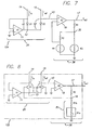
- Fig. 7 shows a logarithmic amplifier 124 including a log amplifier cell 26, the log amplifier cell 26 driving an output stage 36 with a non-inverting amplifier 19 having compound feedback.
- the (+) input of amplifier 19 is connected to conductor 15.
- the output of amplifier 19 is connected by output conductor 17 to one terminal of a resistor R4, the other terminal of which is connected by conductive 30 to 1 terminal of a resistor R2 and to one terminal of a temperature-dependent resistor R3.
- the other terminal of temperature-dependent resistor R3 is connected to ground.
- the other terminal of resistor R2 is connected to the (-) input of amplifier 19 and to one terminal of another temperature-dependent resistor R1, the other terminal of which is connected to ground.
- resistor R1 could be implemented by a P-type diffused resistor (with a temperature coefficient of approximately + 1200 ppm/degrees Centigrade) formed at the same time that the P-type base regions are formed during fabrication of the chip.
- the structure shown in Fig. 7 permits the output voltage on conductor 17 to be divided down by two or more successive voltage dividers, as shown, to a very low feedback voltage on the (-) input of amplifier 19 by using low-value temperature-dependent resistors R1 and R3 and relatively large value resistors R2 and R4 as shown to form the successive voltage dividers.
- the successive voltage divider structure shown increases the effect of the positive temperature coefficients of resistors R1 and R3, and thereby provides the desired temperature compensation of the logarithmic amplifier 124, using temperature-dependent resistors R2 and R4 having temperature coefficients which are substantially lower than the temperature coefficient of aluminum interconnection metallization material.
- resistors R1 and R3 could be temperature-dependent resistors with positive temperature coefficients, and the gain depends on the resistor ratios.
- Resistor R1 in Fig. 7 can be a single temperature-dependent resistor as shown, or it can be a composite of an aluminum resistor R1a and a thin film resistor R1b as shown in Figs. 1-4 .
- Fig. 8 shows a presently preferred embodiment of a monolithic logarithmic amplifier 125 wherein both the current input conductor 14 and the reference current conductor 15 are held at virtual ground by operational amplifiers 11 and 19, respectively.
- the difference between the logarithmic amplifier of Fig. 8 and the logarithmic amplifier of prior art Fig. 1 is that the prior art logarithmic amplifier is a hybrid integrated circuit device including a discrete thermistor on a separate chip utilized as the temperature-dependent element R1a, whereas the entire logarithmic amplifier 125 of Fig.
- Fig. 8 is provided on a single integrated circuit chip, with its temperature-dependent element R1a composed of a serpentine configuration of the ordinary aluminum interconnect metallization material that also is used throughout the chip for interconnection purposes, the large resistance of R1a notwithstanding.
- the dashed line designates the integrated circuit chip on which the entire logarithmic amplifier is provided, and the symbol for resistor R1a represents a different integrated temperature-dependent than a discrete thermistor R1a shown in prior art Fig. 1 .
- composite temperature-dependent resistor R1 which includes the serpentine aluminum metallization resistor R1a and thin film resistor R1b, is the temperature-dependent resistor.
- the (-) input of operational amplifier 11 is connected to input conductor 14.
- the (+) of operational amplifier 11 is connected to ground.
- the output of operational amplifier 11 is connected by conductor 13 to the emitters of a pair of matched NPN transistors Q1 and Q2.
- the base of transistor Q2 is connected to ground.
- the second operational amplifier 19 has its (+) input connected to ground and its (-) input connected to the reference input conductor 15.
- the output of operational amplifier 19 is connected by output conductor 17 to one terminal of thin film resistor R2.
- resistor R2 The other terminal of resistor R2 is connected by conductor 16 to the base of transistor Q1 and to one terminal of composite resistor R1, the other terminal of which is connected to ground.
- V out k * Ln I in / I ref , where k is a scale factor.
- Fig. 9 is a plan view of logarithmic amplifier 125 of Fig. 8 , implemented on a single integrated circuit chip.
- the locations of most of the circuitry of operational amplifiers 11 and 19 are indicated by reference characters A1 and A2, respectively.
- Areas 11A and 19A designate the locations of a pair of auxiliary amplifiers that can be used if desired.
- the locations of transistors Q1 and Q2 are indicated.
- the serpentine aluminum metallization resistor R1a is located in the available areas of the chip designated by the characters R1a in Fig. 9 .
- the serpentine aluminum metallization resistor R1a occupies roughly 10 percent of the area of the integrated circuit chip. However, aluminum metallization resistor R1a does not need to be configured in the same serpentine fashion illustrated in Fig.
- the same length of metallization material could be laid out as a loop or spiral configuration or the like either within or “looped around" a peripheral portion of the integrated circuit chip.
- the term “serpentine” as used herein is intended to encompass both a generally “spiraled” configuration of the metallization material and a “non-spiraled” configuration as illustrated in Fig. 9 .
- the invention provides a versatile integrated circuit logarithmic and log ratio amplifier that produces the logarithm, log ratio or anti-log of an input current or input voltage relative to a reference current or reference voltage with high precision over a wide dynamic range of input signals.
- the drift of the kT/q term of the transistors Q1 and Q2 or diodes D1 and D2 is canceled, i.e. compensated, by the use of one or more relatively large-value resistors composed only of the standard aluminum or aluminum alloy metallization utilized as the integrated circuit interconnection metallization during processing of the integrated circuit wafers.
- the described small, low-cost temperature-compensated logarithmic amplifier is especially useful for measurement of light intensities in fiber-optic devices.
- the temperature-dependent resistor element could be composed of other interconnection metal or alloy metal material than the aluminum metallization and aluminum alloy metallization described above.
- the temperature-dependent resistor element also could be composed of doped silicon or doped polycrystalline silicon material.
- the PN junctions can be PN junctions of silicon transistors, and the diodes D1 and D2 can be diode-connected transistors.
- the semiconductor junctions can be provided as a different combination of silicon diodes and silicon transistors.
- the semiconductor junctions can be provided as a transistor Q1 and a diode D2 as indicated by the dotted line structure of Q1 shown in Fig. 5 .
- the disclosed logarithmic amplifier circuits can be easily modified so that the input current I in flows out of rather than into input terminal 14, and the reference current I ref flows out of rather than into reference terminal 15.
- the high temperature coefficient interconnection material does not necessarily have to be metallization material.
- the high temperature coefficient interconnection material can be doped silicon interconnection material (such as P-type doped silicon material or N-type doped silicon material) or doped polycrystalline silicon interconnection material that is provided on the chip during fabrication thereof.
Description
- The invention relates to monolithic logarithmic amplifier integrated circuits and to methods for logarithmic conversion of an input signal.
- Logarithmic amplifiers have been used to provide various functions. The closest prior art is believed to be the assignee's hybrid integrated circuit LOG100 logarithmic and log ratio amplifier, the article "What's All This Logarithmic Stuff, Anyhow?", by Robert A. Pease, Electronic Design, June 14, 1989, pp. 111-113. Also see the text "Function Circuits" by Wong and Ott, McGraw-Hill Publishing Company, New York, 1976, page 58. Logarithmic amplifiers have been used in signal compression wherein the compressive effects of the logarithmic transfer function are useful. For example, use of the assignee's LOG100 logarithmic amplifier connected ahead of an eight-bit analog-to-digital converter can produce equivalent 20-bit converter dynamic range.
-
Fig. 1 is a schematic diagram of the assignee's above mentioned hybrid integrated circuit LOG100 logarithmic amplifier. Referring toFig. 1 , thelogarithmic amplifier 1A includes a first operational amplifier 11 (also referred to as operational amplifier A1) having its (-) input connected to anexternal input terminal 14 into which an input current Iin is provided by the user. The (+) input ofoperational amplifier 11 is connected to ground. The output ofoperational amplifier 11 is connected byconductor 13 to the emitter of an NPN transistor Q1, the collector of which is connected toinput terminal 14. The emitter of transistor Q1 is also connected byconductor 13 to the emitter of a matched NPN transistor Q2 having its base connected to ground and its collector connected to both an externalreference current terminal 15 into which a reference current Iref is supplied by the user, and to the (-) input of a second operational amplifier 19 (also referred to as operational amplifier A2) having its (+) input connected to ground. The output ofoperational amplifier 19 is connected to anexternal output conductor 17 on which an output voltage Vout representative of the log ratio of Iin/Iref is produced. The base of transistor Q1 is connected to anexternal terminal 16. Vout is connected to one terminal of a thin film resistor R2, the other terminal of which is connected toconductor 16. A "composite" temperature-dependent resistor R1 having a large positive temperature coefficient (TC) is coupled betweenconductor 16 and ground. Resistor R1 includes a 270 ohm thin film resistor R1b connected betweenconductor 16 and one terminal of a 220 ohm thermistor R1a, the other terminal of which is connected to ground. Composite resistor R2 may be a selectable parallel combination of thin film resistors each of which has one terminal connected toterminal 16 and another terminal connected to enable the user to set the resistance of R2. -
Logarithmic amplifier 1A ofFig. 1 is implemented as a hybrid integrated circuit. The thermistor R1a is formed on a discrete chip that is bonded onto the hybrid integrated circuit. Because of its large size, the logarithmic amplifier 1 of prior artFig. 1 must be packaged in a larger package. -
Fig. 2 shows a schematic diagram of another prior artlogarithmic amplifier 1B similar to that ofFig. 1 except that transistors Q1 and Q2 have been replaced by (or are represented by) diodes D1 and D2, respectively. - Generally, it is more convenient and less expensive to integrate all the elements of a circuit into a single chip. Furthermore, monolithic construction also facilitates assembly of the circuit into small surface mount packages, such as the SO-14. Accordingly, the prior art logarithmic amplifier shown in
Fig. 1 has the disadvantages that the hybrid LOG100 product is not "compatible with" ordinary monolithic integrated circuit (IC) technology. However, adding the capability of providing a conventional thermistor in a conventional IC process would have resulted in additional complexity and cost. - Thus, the LOG100 design shown in
Fig. 1 was considered impractical to implement on a single chip, because a thermistor which could, as a practical matter, have been provided on the same chip along with the amplifier circuitry and thin film resistors, was not available. It would have been considered impractical, in view of the benefit, to add the semiconductor processing steps that would have been needed to include a thermistor in a single-chip implementation of the LOG100. - Until now no one has provided a logarithmic amplifier similar to the ones shown in
Figs. 1 and 2 integrated into a single monolithic chip and capable of being packaged in a small, inexpensive plastic package, such as a TSSOP-14 or a SO-14. - In the past, integrated circuit interconnection metallization generally has only been utilized for making very low resistance resistors. For example, very low value resistors, e.g., emitter resistors and shunt resistors having very small resistances have been formed of the integrated circuit interconnection metallization that also is used throughout the integrated circuit.
U.S. patent 4,990,803 (Gilbert) issued Feb. 5th, 1981 discloses a multi-stage logarithmic amplifier in which a front end PTAT resistive attenuator includes an input voltage divider circuit including a high temperature coefficient resistor and a fixed resistor in its transfer branch. The output of the attenuator is connected to a logarithmic cell circuit. Patent4,990,803 - Thus, there has been a long-standing unmet need for a monolithic temperature-compensated logarithmic amplifier.
- The present invention provides apparatus as set forth in the claims.
-
-
Fig. 1 is a schematic diagram of a prior art logarithmic amplifier. -
Fig. 2 is a schematic diagram of another prior art logarithmic amplifier. -
Fig. 3 is a schematic diagram of a logarithmic amplifier according to the present invention, having a current input signal. -
Fig. 4 is a schematic diagram of a logarithmic amplifier of the present invention, having a voltage input signal. -
Fig. 5 is a schematic diagram of a logarithmic amplifier which is a variation of the logarithmic amplifier ofFig. 4 . -
Fig. 6 is a schematic diagram of another logarithmic amplifier of the present invention. -
Fig. 7 is a schematic diagram of another amplifier of the present invention having a non-inverting output amplifier. -
Fig. 8 it is schematic diagram of the preferred logarithmic amplifier of the present invention. -
Fig. 9 is a plan view that approximately illustrating the general layout of the monolithic integrated circuit logarithmic amplifier ofFig. 8 , and the general layout of the serpentine aluminum interconnection metallization resistor R1a. -
Fig. 3 is a schematic diagram of a monolithic integrated circuitlogarithmic amplifier 120 of the present invention.Logarithmic amplifier 120 is similar tologarithmic amplifier 1B of prior artFig. 2 . However, inlogarithmic amplifier 120, all of the circuitry is included on a singlemonolithic chip 120A. Thermistor R1 ofFig. 2 . is replaced by a positive TC resistor R1 which includes a large serpentine aluminum interconnection metallization resistor R1a composed of the same kind of aluminum or aluminum alloy interconnection metallization which is used to fabricate the metal interconnections throughout the chip. (Subsequently describedFig. 9 illustrates the serpentine structure of interconnection metallization resistor R1a.) Positive TC resistor R1 also includes a conventional thin-film resistor R1b. Typically, resistor R2 is a thin film resistor, typically composed of nichrome (NiCr) or sichrome (SiCr), which is essentially temperature-independent. - In one embodiment of the invention, aluminum interconnection metallization resistor R1a has a resistance of approximately 200 ohms, which is very large compared to the resistance of any known aluminum interconnection metallization resistor, and is formed by a large serpentine arrangement of aluminum metallization approximately 0.35 mils wide and approximately 10,000 Angstrom units thick. However, it may be practical for aluminum interconnection metallization resistor R1a to have a lower resistance, perhaps a low as 100 ohms, or even less. The thin film resistors described herein can be composed of nichrome. An exemplary value of resistor R1b is 30 ohms, and a typical value of resistor R2 is 3375 ohms. Typically, the aluminum interconnection metallization resistor R1a occupies approximately 10 percent of the area of the integrated circuit chip on which the logarithmic amplifier is formed. A typical value of Iin is in range of 1 nanoampere to 1 milliampere. A typical value of Iref also is in the range of 1 nanoampere to 1 milliampere.
- As is well known, a semiconductor PN junction, such as a silicon PN junction, can be used as a predictable element for log conversion. The base-emitter voltage of a forward-biased PN junction is a fairly accurate logarithmic function of current across the junction. The voltage across the forward-biased silicon junction is approximated by:

- I = current across the junction
- Is = saturation current of the junction
- q = charge of an electron = 1 eV
- k = Boltzmann's constant = 8.62*10-5 eV/K
- T = absolute temperature (degrees Kelvin (K)).
- V1 =(kT/q) Ln (Iin/Is1),
- V2 =(kT/q) Ln (Iref/Is2),
- V3 = -V1+V2.
- Iin = input current to
logarithmic amplifier 120, - Iref = reference current to
logarithmic amplifier 120, - V3 = output voltage from
logarithmic converter cell 26, - Vout = amplified output voltage of
logarithmic amplifier 120. - Therefore, the output voltage V3 is approximately proportional to the absolute temperature (degrees Kelvin), and has a temperature coefficient (TC) of approximately 1/298 degrees Centigrade or about 3000 ppm/degree Centigrade at room temperature. The first-order correction for the drift of V3 can be provided by arranging for the gain of the amplifier (A2, R1, R2) to have a compensating TC of approximately -3000 ppm per degree Centigrade at 298 degrees Centigrade.
- This can be accomplished by using a resistor with the appropriate positive TC for composite resistor R1. Composite resistor R1 can be composed of the above mentioned aluminum metallization resistor R1a and thin film resistor R1b connected in series, one resistor (e.g., R1b) having lower the lower or zero TC and the other resistor (e.g., R1a) having a TC that is substantially higher than the positive TC (3000 ppm per degree Centigrade) needed for composite resistor R1. By selecting the ratio of resistors R1a and R1b appropriately, a series combination with the needed TC of approximately + 3000 ppm per degree Centigrade can be created. See page 58 of the above referenced Wong and Ott article.
- It should be appreciated that it is much more convenient and much less expensive to manufacture an integrated circuit if all of the circuit elements can be included on the same monolithic chip. (However, in the past the difficulty of including the capability of providing a thermistor in a conventional integrated circuit wafer fabrication process was considered too costly to overcome, so it has been necessary to provide a large, expensive package to accommodate the multiple chips required for the above described prior art LOG100 product.)
- In the described embodiments of the invention, the physically large, positive TC resistor R1a, with a resistance of roughly 200 ohms, is provided by using the same standard aluminum interconnection metallization material that is also used in the semiconductor process to provide interconnection metallization throughout the chip. The aluminum metallization used by the assignee has a positive TC of approximately 4000 ppm/degree Centigrade, which is suitable for this application, as will be shown by the following example. (However, other levels of interconnect metallization commonly used in other integrated circuit manufacturing processes can be used, provided such metallization has the needed temperature coefficient.)
- A convenient gain for the logarithmic converter of
Fig. 3 would be obtained by configuring the logarithmic amplifier output at 1 volt per decade of input current. I.e., if Iref is equal to 10Iin, then Vout = 1 volt. Then, at 298 degrees K (i.e., at room temperature),
V3 = 8.62 *10-5*298 Ln (10) = 0.0591 volts, for 1 volt per decade of input current.
The gain oflog converter cell 36 is equal to 1/0.0591, or 16.9 volts per volt.
Solving for the values of resistors R1 and R2 if in thelogarithmic amplifier 120 ofFig. 3 :
If R1t = R1 (1+tcR1 (t-tnom)), then, assuming no thermal drift of R2,
where - t = temperature
- tnom = nominal temperature, e.g., room temperature
- tcR1 = temperature coefficient of R1.
- g0 = gain of
operational amplifier 19 at t =tnom - gt = gain of
operational amplifier 19 as a function of temperature t. - The conclusion is that temperature compensation at tnom can be achieved with resistors ratioed at the above indicated ranges of values. For example, if we ratio by 1000:
- R1 = 15.9 kilohms (at zero tcr)
- R2 = 1 kilohm (3190 tcr formed from series-connected R1a +R1b)
- R1a = 797.5 ohms (4000 ppm tcr, e.g., for aluminum alloy conductor)
- R1b = 202.5 ohms (at zero tcr).
- Although the
logarithmic amplifier 120 ofFig. 3 is configured to receive an input current signal, various other configurations can be provided to allow use of an input voltage signal Vin. For example,Fig. 4 shows alogarithmic amplifier 121 which is a variation of the circuit ofFig. 3 , modified to receive the voltage input signal Vin on anexternal input conductor 18. An input resistor Rin is connected betweeninput conductor 18 and aninternal conductor 14. Since the voltage at the negative input of operational amplifier A1 is held at virtual ground, the resistor Rin connected byconductor 14 to the (-) input of operational amplifier A1 provides a suitable voltage-to-current conversion such that a current Iin flowing inconductor 14 through diode (or P-N junction) D1 is equal to Vin/Rin. Otherwise,logarithmic amplifier 121 ofFig. 4 is essentially identical tologarithmic amplifier 120 ofFig. 3 . - The
logarithmic amplifier 120 ofFig. 3 is configured with non-inverting amplifier circuitry A2,R1,R2 so as to provide gain and temperature compensation. However, various other logarithmic amplifier circuit configurations also can provide gain and temperature compensation in accordance with the present invention. For example, thelogarithmic amplifier 122 shown inFig. 5 is configured with anoperational amplifier 19 in aninverting gain stage 36A so as to provide both gain and temperature compensation by using resistor R1 as the temperature-dependent resistor. Resistor R1 inFig. 5 can be a single temperature-dependent resistor as shown, or it can be a composite of an aluminum resistor R1a and a thin film resistor R1b as shown inFigs. 1-4 . To accomplish this, abuffer amplifier 21 is coupled betweenconductor 15 and one terminal of temperature-dependent resistor R1. The (+) input ofbuffer amplifier 21 is connected to referenceinput conductor 15. The output ofbuffer amplifier 21 is connected to its (-) input as well as to one terminal of temperature-dependent resistor R1, the other terminal of which is connected byconductor 16 to the (-) input ofoperational amplifier 19 and to one terminal of feedback resistor R2. The (+) input ofoperational amplifier 19 is connected to ground. The output ofoperational amplifier 19 is connected byconductor 17 to the other terminal of feedback resistor R2. - Solving for the gain temperature coefficient tcg of inverting amplifier A2 in
Fig. 5 :


- Using two or more cascaded gain stages can boost overall gain drift so that resistive elements each having lower temperature coefficients (e.g., each having a temperature coefficient less than 1/298) can be used to accomplish temperature compensation of the logarithmic converter. For example,
Fig. 6 shows anotherlogarithmic amplifier 123 that could be formed on a single monolithic chip.Logarithmic amplifier 123 ofFig. 6 is similar tologarithmic amplifier 122 ofFig. 5 , but is modified to include a second cascadedgain stage 38 includingamplifier 25, a feedback resistor R2, and a temperature-dependent resistor R1 connected by conductor 16B, which is connected to the (-) input ofamplifier 25. Second cascadedgain stage 38 can be similar or identical to gainstage 36A, and has its input connected toconductor 22 and its output connected byconductor 26 to the input ofgain stage 36A. In this example, the gain stages 36A and 38 are the same, and the R1 resistors are the temperature-dependent elements. - Solving for the gain temperature coefficient of
logarithmic amplifier 123 inFig. 6 , with the gain divided into two equal-gain cascaded inverting amplifier stages:


Solving for the gain temperature coefficient with the gain divided into "n" equal-gain cascaded inverting amplifier stages:


-
Fig. 7 shows alogarithmic amplifier 124 including alog amplifier cell 26, thelog amplifier cell 26 driving anoutput stage 36 with anon-inverting amplifier 19 having compound feedback. The (+) input ofamplifier 19 is connected toconductor 15. The output ofamplifier 19 is connected byoutput conductor 17 to one terminal of a resistor R4, the other terminal of which is connected by conductive 30 to 1 terminal of a resistor R2 and to one terminal of a temperature-dependent resistor R3. The other terminal of temperature-dependent resistor R3 is connected to ground. The other terminal of resistor R2 is connected to the (-) input ofamplifier 19 and to one terminal of another temperature-dependent resistor R1, the other terminal of which is connected to ground. By using multiple voltage dividers, this type of circuitry allows convenient use of low value resistors having a lower positive temperature coefficient than that of typical aluminum interconnect metallization material. For example, resistor R1 could be implemented by a P-type diffused resistor (with a temperature coefficient of approximately + 1200 ppm/degrees Centigrade) formed at the same time that the P-type base regions are formed during fabrication of the chip. - The structure shown in
Fig. 7 permits the output voltage onconductor 17 to be divided down by two or more successive voltage dividers, as shown, to a very low feedback voltage on the (-) input ofamplifier 19 by using low-value temperature-dependent resistors R1 and R3 and relatively large value resistors R2 and R4 as shown to form the successive voltage dividers. The successive voltage divider structure shown increases the effect of the positive temperature coefficients of resistors R1 and R3, and thereby provides the desired temperature compensation of thelogarithmic amplifier 124, using temperature-dependent resistors R2 and R4 having temperature coefficients which are substantially lower than the temperature coefficient of aluminum interconnection metallization material. (Although the basic operational assertive ofFig. 7 is understood, the mathematical analysis of the circuit ofFig. 7 is much more complex than the analysis for the other circuits disclosed, and has not been completed.) In this configuration, resistors R1 and R3 could be temperature-dependent resistors with positive temperature coefficients, and the gain depends on the resistor ratios. Resistor R1 inFig. 7 can be a single temperature-dependent resistor as shown, or it can be a composite of an aluminum resistor R1a and a thin film resistor R1b as shown inFigs. 1-4 . - Various other circuit configurations can be used to provide the logarithmic conversion functions in the present invention.
-
Fig. 8 shows a presently preferred embodiment of a monolithiclogarithmic amplifier 125 wherein both thecurrent input conductor 14 and the referencecurrent conductor 15 are held at virtual ground byoperational amplifiers Fig. 8 and the logarithmic amplifier of prior artFig. 1 is that the prior art logarithmic amplifier is a hybrid integrated circuit device including a discrete thermistor on a separate chip utilized as the temperature-dependent element R1a, whereas the entirelogarithmic amplifier 125 ofFig. 8 is provided on a single integrated circuit chip, with its temperature-dependent element R1a composed of a serpentine configuration of the ordinary aluminum interconnect metallization material that also is used throughout the chip for interconnection purposes, the large resistance of R1a notwithstanding. InFig. 8 , the dashed line designates the integrated circuit chip on which the entire logarithmic amplifier is provided, and the symbol for resistor R1a represents a different integrated temperature-dependent than a discrete thermistor R1a shown in prior artFig. 1 . - As in
Figs. 3-7 , composite temperature-dependent resistor R1, which includes the serpentine aluminum metallization resistor R1a and thin film resistor R1b, is the temperature-dependent resistor. InFig. 8 , the (-) input ofoperational amplifier 11 is connected to inputconductor 14. The (+) ofoperational amplifier 11 is connected to ground. The output ofoperational amplifier 11 is connected byconductor 13 to the emitters of a pair of matched NPN transistors Q1 and Q2. The base of transistor Q2 is connected to ground. The secondoperational amplifier 19 has its (+) input connected to ground and its (-) input connected to thereference input conductor 15. The output ofoperational amplifier 19 is connected byoutput conductor 17 to one terminal of thin film resistor R2. The other terminal of resistor R2 is connected byconductor 16 to the base of transistor Q1 and to one terminal of composite resistor R1, the other terminal of which is connected to ground. In this configuration:
-
Fig. 9 is a plan view oflogarithmic amplifier 125 ofFig. 8 , implemented on a single integrated circuit chip. The locations of most of the circuitry ofoperational amplifiers Areas Fig. 9 . The serpentine aluminum metallization resistor R1a occupies roughly 10 percent of the area of the integrated circuit chip. However, aluminum metallization resistor R1a does not need to be configured in the same serpentine fashion illustrated inFig. 9 . For example, the same length of metallization material could be laid out as a loop or spiral configuration or the like either within or "looped around" a peripheral portion of the integrated circuit chip. By way of definition, the term "serpentine" as used herein is intended to encompass both a generally "spiraled" configuration of the metallization material and a "non-spiraled" configuration as illustrated inFig. 9 . - The invention provides a versatile integrated circuit logarithmic and log ratio amplifier that produces the logarithm, log ratio or anti-log of an input current or input voltage relative to a reference current or reference voltage with high precision over a wide dynamic range of input signals. The drift of the kT/q term of the transistors Q1 and Q2 or diodes D1 and D2 is canceled, i.e. compensated, by the use of one or more relatively large-value resistors composed only of the standard aluminum or aluminum alloy metallization utilized as the integrated circuit interconnection metallization during processing of the integrated circuit wafers.
- The described small, low-cost temperature-compensated logarithmic amplifier is especially useful for measurement of light intensities in fiber-optic devices.
- The temperature-dependent resistor element could be composed of other interconnection metal or alloy metal material than the aluminum metallization and aluminum alloy metallization described above. For example, the temperature-dependent resistor element also could be composed of doped silicon or doped polycrystalline silicon material. The PN junctions can be PN junctions of silicon transistors, and the diodes D1 and D2 can be diode-connected transistors. The semiconductor junctions can be provided as a different combination of silicon diodes and silicon transistors. For example, the semiconductor junctions can be provided as a transistor Q1 and a diode D2 as indicated by the dotted line structure of Q1 shown in
Fig. 5 . The disclosed logarithmic amplifier circuits can be easily modified so that the input current Iin flows out of rather than intoinput terminal 14, and the reference current Iref flows out of rather than intoreference terminal 15. The high temperature coefficient interconnection material does not necessarily have to be metallization material. For example, the high temperature coefficient interconnection material can be doped silicon interconnection material (such as P-type doped silicon material or N-type doped silicon material) or doped polycrystalline silicon interconnection material that is provided on the chip during fabrication thereof.
where:

R1b 0.2025, R1b 0.7975.
Claims (7)
- A temperature-compensated logarithmic amplifier
circuit, comprising:(a) a logarithmic amplifier cell (26) configured to produce a logarithmic voltage signal (V3) representative of a difference between a first voltage (V1) developed across a first PN junction device (D1) in response to an input (lin) signal and a second voltage (V2) developed across a second PN junction device (D2) in response to a reference signal (Iref); and(b) an output circuit (36) including an output amplifier (19), a temperature-dependent first resistive element (R1) having a positive first temperature coefficient and a second resistive element (R2) having a second temperature coefficient that is of substantially lower magnitude than the first temperature coefficient, the first and second resistive elements being coupled as a voltage divider between an output of the output amplifier and a reference conductor to provide a feedback signal to an input of the output amplifier, the output circuit (36) being configured to produce a temperature-compensated output signal (Vout) in response to the logarithmic voltage signal,- wherein the logarithmic voltage signal (V3) is applied to the input of the output amplifier (19),characterised in that:- the temperature-compensated logarithmic amplifier is a monolithic circuit,- the first resistive element (R1) includes interconnection metallization material formed on the monolithic logarithmic amplifier circuit simultaneously with formation of interconnection metallization elsewhere on the monolithic logarithmic amplifier circuit, and- the interconnection metallization material of the first resistive element (R1) being configured as an elongate structure of sufficiently high resistance to temperature-compensate the logarithmic voltage signal. - The temperature-compensated logarithmic amplifier circuit of claim 1 wherein the first resistive element is at least partially configured as a serpentine structure.
- The temperature-compensated logarithmic amplifier circuit of claims 1 or 2 wherein the conductive material is aluminum interconnection metallization material.
- The temperature-compensated logarithmic amplifier circuit of claim 1 or claim 2 wherein the conductive material is aluminum alloy interconnection metallization material.
- The temperature-compensated logarithmic amplifier circuit of claim 4 wherein a temperature coefficient of the aluminum alloy interconnection metallization material is approximately + 4000 ppm per degree Centigrade.
- The temperature-compensated logarithmic amplifier circuit of any preceding claim wherein a resistance of the first resistive element is greater than approximately 100 ohms.
- The temperature-compensated logarithmic amplifier circuit of any preceding claim wherein the second resistive element is composed of thin film resistive material.
Applications Claiming Priority (2)
| Application Number | Priority Date | Filing Date | Title |
|---|---|---|---|
| US920220 | 1992-07-24 | ||
| US09/920,220 US6507233B1 (en) | 2001-08-02 | 2001-08-02 | Method and circuit for compensating VT induced drift in monolithic logarithmic amplifier |
Publications (3)
| Publication Number | Publication Date |
|---|---|
| EP1282064A2 EP1282064A2 (en) | 2003-02-05 |
| EP1282064A3 EP1282064A3 (en) | 2004-12-01 |
| EP1282064B1 true EP1282064B1 (en) | 2009-12-23 |
Family
ID=25443372
Family Applications (1)
| Application Number | Title | Priority Date | Filing Date |
|---|---|---|---|
| EP02102091A Expired - Fee Related EP1282064B1 (en) | 2001-08-02 | 2002-08-02 | Method and circuit for compensating vt inducted drift in monolithic logarithmic amplifier |
Country Status (4)
| Country | Link |
|---|---|
| US (1) | US6507233B1 (en) |
| EP (1) | EP1282064B1 (en) |
| JP (1) | JP2003078357A (en) |
| DE (1) | DE60234797D1 (en) |
Families Citing this family (8)
| Publication number | Priority date | Publication date | Assignee | Title |
|---|---|---|---|---|
| KR100393226B1 (en) * | 2001-07-04 | 2003-07-31 | 삼성전자주식회사 | Internal reference voltage generator capable of controlling value of internal reference voltage according to temperature variation and internal power supply voltage generator including the same |
| US6759892B2 (en) * | 2002-03-25 | 2004-07-06 | Texas Instruments Incorporated | Temperature compensation trim method |
| US20080063027A1 (en) * | 2006-03-15 | 2008-03-13 | Giovanni Galli | Precision temperature sensor |
| US20090285261A1 (en) * | 2008-05-17 | 2009-11-19 | Lsi Corporation | Integrated Circuit System Monitor |
| KR20110063668A (en) * | 2008-09-30 | 2011-06-13 | 가부시키가이샤 한도오따이 에네루기 켄큐쇼 | Semiconductor device |
| US8676521B2 (en) * | 2009-10-26 | 2014-03-18 | Fluke Corporation | System and method for handling wide dynamic range signals encountered in vibration analysis using a logarithmic amplifier |
| US8004341B1 (en) * | 2010-04-30 | 2011-08-23 | Analog Devices, Inc. | Logarithmic circuits |
| US11385267B2 (en) * | 2019-02-14 | 2022-07-12 | Psemi Corporation | Power detector with wide dynamic range |
Family Cites Families (6)
| Publication number | Priority date | Publication date | Assignee | Title |
|---|---|---|---|---|
| US4990803A (en) | 1989-03-27 | 1991-02-05 | Analog Devices, Inc. | Logarithmic amplifier |
| US5471132A (en) * | 1991-09-30 | 1995-11-28 | Sgs-Thomson Microelectronics, Inc. | Logarithmic and exponential converter circuits |
| US5481218A (en) * | 1994-09-30 | 1996-01-02 | Telefonaktiebolaget Lm Ericsson | Logarithmic converter |
| US5805011A (en) * | 1997-01-03 | 1998-09-08 | Lucent Technologies Inc. | Self-calibration system for logarithmic amplifiers |
| US5877645A (en) * | 1997-08-08 | 1999-03-02 | Lucent Technologies Inc. | Offset compensation circuit for integrated logarithmic amplifiers |
| US6229375B1 (en) * | 1999-08-18 | 2001-05-08 | Texas Instruments Incorporated | Programmable low noise CMOS differentially voltage controlled logarithmic attenuator and method |
-
2001
- 2001-08-02 US US09/920,220 patent/US6507233B1/en not_active Expired - Lifetime
-
2002
- 2002-08-02 EP EP02102091A patent/EP1282064B1/en not_active Expired - Fee Related
- 2002-08-02 JP JP2002225816A patent/JP2003078357A/en active Pending
- 2002-08-02 DE DE60234797T patent/DE60234797D1/en not_active Expired - Lifetime
Also Published As
| Publication number | Publication date |
|---|---|
| EP1282064A2 (en) | 2003-02-05 |
| JP2003078357A (en) | 2003-03-14 |
| US6507233B1 (en) | 2003-01-14 |
| EP1282064A3 (en) | 2004-12-01 |
| DE60234797D1 (en) | 2010-02-04 |
Similar Documents
| Publication | Publication Date | Title |
|---|---|---|
| US5774013A (en) | Dual source for constant and PTAT current | |
| US6828847B1 (en) | Bandgap voltage reference circuit and method for producing a temperature curvature corrected voltage reference | |
| US5900772A (en) | Bandgap reference circuit and method | |
| EP0429198B1 (en) | Bandgap reference voltage circuit | |
| US6225850B1 (en) | Series resistance compensation in translinear circuits | |
| US6351111B1 (en) | Circuits and methods for providing a current reference with a controlled temperature coefficient using a series composite resistor | |
| US6426669B1 (en) | Low voltage bandgap reference circuit | |
| US4329639A (en) | Low voltage current mirror | |
| JPS6269306A (en) | Temperature compensation cmos voltage reference circuit | |
| EP0072589B1 (en) | Current stabilizing arrangement | |
| US6759893B2 (en) | Temperature-compensated current source | |
| US4763028A (en) | Circuit and method for semiconductor leakage current compensation | |
| EP1282064B1 (en) | Method and circuit for compensating vt inducted drift in monolithic logarithmic amplifier | |
| US20030123520A1 (en) | Temperature detector | |
| Lin et al. | AV/SUB be/(T) model with application to bandgap reference design | |
| US5051686A (en) | Bandgap voltage reference | |
| US4618833A (en) | Operational amplifier offset trim that does not change the offset potential temperature drift | |
| US6310510B1 (en) | Electronic circuit for producing a reference current independent of temperature and supply voltage | |
| US20040196073A1 (en) | Voltage detection circuit | |
| US6605987B2 (en) | Circuit for generating a reference voltage based on two partial currents with opposite temperature dependence | |
| KR19990008200A (en) | Reference voltage source with temperature compensation | |
| EP0618658B1 (en) | Thermal protection circuit | |
| US4336494A (en) | Insulation resistance tester | |
| EP0539136B1 (en) | Voltage generating device | |
| US6566721B2 (en) | Semiconductor device |
Legal Events
| Date | Code | Title | Description |
|---|---|---|---|
| PUAI | Public reference made under article 153(3) epc to a published international application that has entered the european phase |
Free format text: ORIGINAL CODE: 0009012 |
|
| AK | Designated contracting states |
Designated state(s): AT BE BG CH CY CZ DE DK EE ES FI FR GB GR IE IT LI LU MC NL PT SE SK TR |
|
| AX | Request for extension of the european patent |
Extension state: AL LT LV MK RO SI |
|
| PUAL | Search report despatched |
Free format text: ORIGINAL CODE: 0009013 |
|
| AK | Designated contracting states |
Kind code of ref document: A3 Designated state(s): AT BE BG CH CY CZ DE DK EE ES FI FR GB GR IE IT LI LU MC NL PT SE SK TR |
|
| AX | Request for extension of the european patent |
Extension state: AL LT LV MK RO SI |
|
| RIC1 | Information provided on ipc code assigned before grant |
Ipc: 7G 06G 7/24 A Ipc: 7H 03F 1/30 B |
|
| 17P | Request for examination filed |
Effective date: 20050601 |
|
| AKX | Designation fees paid |
Designated state(s): DE FR GB |
|
| GRAP | Despatch of communication of intention to grant a patent |
Free format text: ORIGINAL CODE: EPIDOSNIGR1 |
|
| GRAS | Grant fee paid |
Free format text: ORIGINAL CODE: EPIDOSNIGR3 |
|
| GRAA | (expected) grant |
Free format text: ORIGINAL CODE: 0009210 |
|
| AK | Designated contracting states |
Kind code of ref document: B1 Designated state(s): DE FR GB |
|
| REG | Reference to a national code |
Ref country code: GB Ref legal event code: FG4D |
|
| REF | Corresponds to: |
Ref document number: 60234797 Country of ref document: DE Date of ref document: 20100204 Kind code of ref document: P |
|
| PLBE | No opposition filed within time limit |
Free format text: ORIGINAL CODE: 0009261 |
|
| STAA | Information on the status of an ep patent application or granted ep patent |
Free format text: STATUS: NO OPPOSITION FILED WITHIN TIME LIMIT |
|
| 26N | No opposition filed |
Effective date: 20100924 |
|
| REG | Reference to a national code |
Ref country code: FR Ref legal event code: PLFP Year of fee payment: 15 |
|
| REG | Reference to a national code |
Ref country code: FR Ref legal event code: PLFP Year of fee payment: 16 |
|
| PGFP | Annual fee paid to national office [announced via postgrant information from national office to epo] |
Ref country code: GB Payment date: 20170725 Year of fee payment: 16 Ref country code: FR Payment date: 20170720 Year of fee payment: 16 Ref country code: DE Payment date: 20170825 Year of fee payment: 16 |
|
| REG | Reference to a national code |
Ref country code: DE Ref legal event code: R119 Ref document number: 60234797 Country of ref document: DE |
|
| GBPC | Gb: european patent ceased through non-payment of renewal fee |
Effective date: 20180802 |
|
| PG25 | Lapsed in a contracting state [announced via postgrant information from national office to epo] |
Ref country code: DE Free format text: LAPSE BECAUSE OF NON-PAYMENT OF DUE FEES Effective date: 20190301 |
|
| PG25 | Lapsed in a contracting state [announced via postgrant information from national office to epo] |
Ref country code: FR Free format text: LAPSE BECAUSE OF NON-PAYMENT OF DUE FEES Effective date: 20180831 |
|
| PG25 | Lapsed in a contracting state [announced via postgrant information from national office to epo] |
Ref country code: GB Free format text: LAPSE BECAUSE OF NON-PAYMENT OF DUE FEES Effective date: 20180802 |