EP1281998A1 - Temperature controlled light modulator assembly - Google Patents
Temperature controlled light modulator assembly Download PDFInfo
- Publication number
- EP1281998A1 EP1281998A1 EP01306522A EP01306522A EP1281998A1 EP 1281998 A1 EP1281998 A1 EP 1281998A1 EP 01306522 A EP01306522 A EP 01306522A EP 01306522 A EP01306522 A EP 01306522A EP 1281998 A1 EP1281998 A1 EP 1281998A1
- Authority
- EP
- European Patent Office
- Prior art keywords
- modulator
- modulating
- assembly according
- medium
- laser
- Prior art date
- Legal status (The legal status is an assumption and is not a legal conclusion. Google has not performed a legal analysis and makes no representation as to the accuracy of the status listed.)
- Granted
Links
- 238000010521 absorption reaction Methods 0.000 claims abstract description 24
- 238000010438 heat treatment Methods 0.000 claims abstract description 13
- 230000005684 electric field Effects 0.000 claims abstract description 12
- 230000001419 dependent effect Effects 0.000 claims abstract description 7
- 239000000758 substrate Substances 0.000 claims description 9
- 229910052782 aluminium Inorganic materials 0.000 claims description 5
- 239000004411 aluminium Substances 0.000 claims description 4
- XAGFODPZIPBFFR-UHFFFAOYSA-N aluminium Chemical compound [Al] XAGFODPZIPBFFR-UHFFFAOYSA-N 0.000 claims description 4
- 230000008033 biological extinction Effects 0.000 claims description 3
- 239000003989 dielectric material Substances 0.000 claims description 3
- 229910052751 metal Inorganic materials 0.000 claims description 3
- 150000001875 compounds Chemical class 0.000 claims description 2
- 230000005693 optoelectronics Effects 0.000 abstract description 3
- 239000004065 semiconductor Substances 0.000 description 12
- 239000000463 material Substances 0.000 description 7
- 230000003287 optical effect Effects 0.000 description 7
- GPXJNWSHGFTCBW-UHFFFAOYSA-N Indium phosphide Chemical compound [In]#P GPXJNWSHGFTCBW-UHFFFAOYSA-N 0.000 description 3
- 239000013590 bulk material Substances 0.000 description 2
- BASFCYQUMIYNBI-UHFFFAOYSA-N platinum Chemical compound [Pt] BASFCYQUMIYNBI-UHFFFAOYSA-N 0.000 description 2
- 229920000642 polymer Polymers 0.000 description 2
- 230000006641 stabilisation Effects 0.000 description 2
- 239000010409 thin film Substances 0.000 description 2
- 229910000980 Aluminium gallium arsenide Inorganic materials 0.000 description 1
- 229910001218 Gallium arsenide Inorganic materials 0.000 description 1
- 229910003327 LiNbO3 Inorganic materials 0.000 description 1
- 238000000862 absorption spectrum Methods 0.000 description 1
- 229910052787 antimony Inorganic materials 0.000 description 1
- 229910052785 arsenic Inorganic materials 0.000 description 1
- 239000000919 ceramic Substances 0.000 description 1
- 238000001816 cooling Methods 0.000 description 1
- 230000008878 coupling Effects 0.000 description 1
- 238000010168 coupling process Methods 0.000 description 1
- 238000005859 coupling reaction Methods 0.000 description 1
- 230000000694 effects Effects 0.000 description 1
- 229910052733 gallium Inorganic materials 0.000 description 1
- 239000011521 glass Substances 0.000 description 1
- 230000017525 heat dissipation Effects 0.000 description 1
- 229910052738 indium Inorganic materials 0.000 description 1
- 230000010354 integration Effects 0.000 description 1
- 239000002184 metal Substances 0.000 description 1
- 238000012544 monitoring process Methods 0.000 description 1
- -1 of In Chemical class 0.000 description 1
- 239000013307 optical fiber Substances 0.000 description 1
- 230000003647 oxidation Effects 0.000 description 1
- 238000007254 oxidation reaction Methods 0.000 description 1
- 229910052698 phosphorus Inorganic materials 0.000 description 1
- 229910052697 platinum Inorganic materials 0.000 description 1
- 230000005701 quantum confined stark effect Effects 0.000 description 1
- 238000000411 transmission spectrum Methods 0.000 description 1
Images


Classifications
-
- G—PHYSICS
- G02—OPTICS
- G02F—OPTICAL DEVICES OR ARRANGEMENTS FOR THE CONTROL OF LIGHT BY MODIFICATION OF THE OPTICAL PROPERTIES OF THE MEDIA OF THE ELEMENTS INVOLVED THEREIN; NON-LINEAR OPTICS; FREQUENCY-CHANGING OF LIGHT; OPTICAL LOGIC ELEMENTS; OPTICAL ANALOGUE/DIGITAL CONVERTERS
- G02F1/00—Devices or arrangements for the control of the intensity, colour, phase, polarisation or direction of light arriving from an independent light source, e.g. switching, gating or modulating; Non-linear optics
- G02F1/01—Devices or arrangements for the control of the intensity, colour, phase, polarisation or direction of light arriving from an independent light source, e.g. switching, gating or modulating; Non-linear optics for the control of the intensity, phase, polarisation or colour
- G02F1/015—Devices or arrangements for the control of the intensity, colour, phase, polarisation or direction of light arriving from an independent light source, e.g. switching, gating or modulating; Non-linear optics for the control of the intensity, phase, polarisation or colour based on semiconductor elements having potential barriers, e.g. having a PN or PIN junction
-
- H—ELECTRICITY
- H01—ELECTRIC ELEMENTS
- H01S—DEVICES USING THE PROCESS OF LIGHT AMPLIFICATION BY STIMULATED EMISSION OF RADIATION [LASER] TO AMPLIFY OR GENERATE LIGHT; DEVICES USING STIMULATED EMISSION OF ELECTROMAGNETIC RADIATION IN WAVE RANGES OTHER THAN OPTICAL
- H01S5/00—Semiconductor lasers
- H01S5/02—Structural details or components not essential to laser action
- H01S5/026—Monolithically integrated components, e.g. waveguides, monitoring photo-detectors, drivers
- H01S5/0265—Intensity modulators
-
- G—PHYSICS
- G02—OPTICS
- G02F—OPTICAL DEVICES OR ARRANGEMENTS FOR THE CONTROL OF LIGHT BY MODIFICATION OF THE OPTICAL PROPERTIES OF THE MEDIA OF THE ELEMENTS INVOLVED THEREIN; NON-LINEAR OPTICS; FREQUENCY-CHANGING OF LIGHT; OPTICAL LOGIC ELEMENTS; OPTICAL ANALOGUE/DIGITAL CONVERTERS
- G02F1/00—Devices or arrangements for the control of the intensity, colour, phase, polarisation or direction of light arriving from an independent light source, e.g. switching, gating or modulating; Non-linear optics
- G02F1/01—Devices or arrangements for the control of the intensity, colour, phase, polarisation or direction of light arriving from an independent light source, e.g. switching, gating or modulating; Non-linear optics for the control of the intensity, phase, polarisation or colour
- G02F1/0147—Devices or arrangements for the control of the intensity, colour, phase, polarisation or direction of light arriving from an independent light source, e.g. switching, gating or modulating; Non-linear optics for the control of the intensity, phase, polarisation or colour based on thermo-optic effects
Definitions
- the present invention relates to a modulator assembly for modulation of light, in particular for use as part of an opto-electronic communication network.
- an opto-electronic communication network it is desirable to produce high frequency modulated light.
- One way of achieving this is to pass light of initially constant intensity through a modulator.
- the modulator is formed using a modulator medium whose optical properties depend on an electric field applied across it, so that modulating the electric field across the modulator medium results in a modulation in the intensity of light passing through it.
- modulators used to modulate light from a laser include electro-absorption modulators, Mach-Zender interferometer modulators, and Fabry-Perot modulators.
- the modulator is normally biased with a quiescent voltage in order to bring it into an operating mode where an absorption edge of the modulator medium is close to the wavelength of the light being modulated.
- a modulation voltage is superimposed onto the quiescent voltage in order to modulate the intensity of light passing through the modulator medium.
- the quiescent voltage normally being constant in time or slowly varying compared to the modulation voltage since it need only change with changing material properties of the modulator medium e.g. with temperature.
- the absorption/transmission spectra of materials usually suitable for modulator media change with temperature, owing to changes in the semiconductor bandgap of the modulator material, changes in the cavity refractive index or changes in the geometrical thickness of the device.
- the absorption edge of an electro-absorption modulator is known to change by around 0.4nm/K whereas the operating wavelength of a typical single mode distributed feedback lasers changes only at around 0.07nm/K.
- thermoelectric cooler thermoelectric cooler
- a light modulator assembly comprising a modulator element comprising a modulating medium, for modulating the intensity of light passing therethrough; and means for applying an electric field across the modulating medium, the modulating medium having an absorption edge at a wavelength dependent upon the temperature of the medium and upon the applied electric field; and means for heating the modulating medium such that the wavelength of the absorption edge aligns with the wavelength of the light to be modulated.
- the means for heating the modulating medium comprises a metallic element in close proximity to the modulating element and advantageously the means for applying an electric field comprises an electrode, which also constitutes the means for heating the modulating medium.
- the device may also comprise a thermally insulating layer of low thermal conductivity and my also have slots each side of the modulating medium.
- modulated light source comprising a laser and a modulator assembly in which the laser and the modulator element may be formed on a common substrate as a monolithic device, or may be secured to a common chip carrier
- Figure 1 shows a known device in which a laser 1 and a modulating element 2 are monolithically integrated (i.e. formed on a common substrate 7).
- the modulating element 2 has a modulating medium with an absorption edge, the wavelength at which the absorption edge occurs being dependent upon an electric field applied across the modulating medium. The wavelength at which the absorption edge occurs is also dependent upon the temperature of the modulating medium.
- a quiescent voltage is applied to the modulating medium such that the wavelength at which the absorption edge occurs is close to the wavelength of the light produced by the laser (typically around 1300nm or 1550 nm), with the result that a small modulating voltage superimposed on the quiescent voltage will cause a significant modulation in the amount of light that is able to pass through the modulator element.
- the device requires temperature stabilisation in order to keep the modulator performance aligned to that of the laser.
- a modulated signal 3 is generated by application of a modulating voltage across the modulating element 2.
- the temperature is stabilised using a thermoelectric cooler 4 driven by a control circuit 5, which monitors the temperature of the laser and modulating element using a thermistor or other temperature sensing element 6.
- the substrate 7 serves to mechanically support the device and ensure that the temperature of the temperature sensing element 6 is similar to that of the laser 1 and modulator 2.
- the laser and modulating element are co-packaged with coupling performed by a lens.
- Another option is for the laser and modulating element to be separately packaged each with their own thermal stabilisation means.
- FIG. 2 illustrates a first embodiment of the present invention in which an electro-absorption modulator 22 having a modulating medium (not shown) is monolithically integrated with a semiconductor laser 21.
- a heater element 8 is in close proximity to the modulator 22 to control the temperature of the modulator 22 essentially independently of that of the laser 21. As the heating element 8 is close to the modulating medium, very little power is required to maintain the temperature of the modulating medium at a desired temperature above the ambient temperature of the substrate 27.
- Temperature sensors 9 and 10 are used to measure the temperatures of the laser and the modulating medium.
- the sensors may each be a thin film sensor such as a platinum resistance thermometer, or a semiconductor sensor, the semiconductor sensor being for example a p-n junction or a thermistor.
- the absorption edge of the modulator 22 is matched to that of the laser 21 by applying heat to the modulator 22 to fix its temperature above the upper temperature of the temperature range of operation of the laser.
- the laser 21 will heat up during use or its temperature will change as a consequence of ambient temperature variations, with the result that the wavelength of the light it produces will change.
- the temperature of the modulator 22 may be controlled to compensate for the variation in wavelength the light from the laser 21.
- the temperature may be fixed if the incoming light wavelength is sufficiently stable over the whole operating temperature range.
- the modulating medium is formed from a semiconductor material.
- the semiconductor material is a bulk material, therefore the absorption edge is the band edge of the bulk material, the wavelength of the band edge being electric field dependent according to the Franz-Keldysch effect.
- the modulating medium may be formed from a plurality of layers, such as a multiple quantum well structure, and the field dependence of the absorption edge is due to the Quantum Confined Stark Effect.
- the laser may also be formed from a plurality of different semiconductor layers.
- the different layers of semiconductor in the modulating medium and/or the laser may be formed from compounds including of In, Ga, As, Al, Sb or P in different proportions, for example GaAs/AlGaAs, InP/Ga(Al)InAsP.
- LiNbO3 polymers, or other materials with a high electro-optic coefficient may also be used.
- an electro-absorption modulator is used.
- Fabry-Perot resonator modulators and Mach-Zender interferometer modulators may be used in other embodiments of the invention.
- the laser and modulator do not need to be integrated as shown in Figure 2; it is sufficient to be able to measure their relative temperatures in order to maintain alignment of the absorption edge by control of the temperature of the modulating element.
- FIG 3 an embodiment of the modulator assembly of this invention is illustrated in which an electrode 13 is used for application of the quiescent voltage together with the modulating voltage across the modulating element 22, the voltage being applied between the electrode 13 and the substrate 12.
- the electrode 13 constitutes the heating element and comprises a thin film metallic heater.
- the heating current is provided by passing a current along the length of the modulator electrode 13.
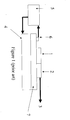
- Figure 4 illustrates a plan view of the modulating element of Figure 3 along with associated control circuitry.
- Control circuit 14 is used to provide the modulation signal for the modulating element 22 and control circuit 15 provides the heating current in dependence upon an output from the temperature sensor 10.
- Figure 5 illustrates a further embodiment of the modulating element of this invention, the modulating element has a semiconductor insulating layer 17 of low thermal conductivity, below an electrically conducting layer 16 which serves as an electrode for application of the quiescent and modulating voltage across the modulating element.
- the insulating layer is designed to decouple the heated section from the substrate, allowing the drive current to be minimised.
- thermally insulating semiconducting materials for devices fabricated on indium phosphide substrates are AlInAs or GaInAlAs as such materials have lower thermal conductivity than indium phosphide.
- the insulating layer may be fabricated from a dielectric material (i.e. an electrically insulating layer which is neither a metal nor a semiconductor).
- a dielectric material i.e. an electrically insulating layer which is neither a metal nor a semiconductor.
- an oxide of aluminium which may be conveniently formed by the steam oxidation of layers of aluminium containing semiconductors.
- a further example is a polymer modulator formed on a low thermal conductivity substrate such as glass or ceramic.
- Figure 6 illustrates modulator assembly according to a further embodiment of the invention in which etched slots 18 are provided close to the modulating medium 11 in order to inhibit loss of heat from the modulating element. Etched slots 18 may be used together with an insulating layer 17, as illustrated, or may be used without such a layer.
- Figure 7 is a plan view of the modulating assembly of Figure 6.
- the invention may be implemented by integration of a laser and a modulator assembly as shown in Figure 2.
- a laser and a modulator may be secured to a common chip carrier and co-packaged.
- a laser is mounted on a chip carrier, and the modulating element is mounted on a second chip carrier allowing the modulator to be run at much higher temperatures than the laser can easily withstand (for example up to 125°C).
- the devices may be coupled by an optical fibre.
- the absorption edge of the modulating element is aligned for optimum performance by monitoring the extinction ratio of the photocurrent which is induced in the modulator.
- the extinction ratio of the photocurrent is the ratio between the photocurrent induced by an optical signal when the optical signal is passing through the modulator (the on state), and the photocurrent induced by an optical signal when the optical signal is absorbed by the modulator (the off state).
- the drive current to the heating element is set at a level which maximises this ratio and hence maximises the ratio between the optical signal which passes through the modulator in the on state, and the optical signal which passes through the modulator in the off state.
Landscapes
- Physics & Mathematics (AREA)
- General Physics & Mathematics (AREA)
- Optics & Photonics (AREA)
- Nonlinear Science (AREA)
- Condensed Matter Physics & Semiconductors (AREA)
- Electromagnetism (AREA)
- Optical Modulation, Optical Deflection, Nonlinear Optics, Optical Demodulation, Optical Logic Elements (AREA)
Abstract
Description
- The present invention relates to a modulator assembly for modulation of light, in particular for use as part of an opto-electronic communication network.
- In an opto-electronic communication network, it is desirable to produce high frequency modulated light. One way of achieving this is to pass light of initially constant intensity through a modulator. Normally the modulator is formed using a modulator medium whose optical properties depend on an electric field applied across it, so that modulating the electric field across the modulator medium results in a modulation in the intensity of light passing through it. Examples of modulators used to modulate light from a laser include electro-absorption modulators, Mach-Zender interferometer modulators, and Fabry-Perot modulators.
- The modulator is normally biased with a quiescent voltage in order to bring it into an operating mode where an absorption edge of the modulator medium is close to the wavelength of the light being modulated. A modulation voltage is superimposed onto the quiescent voltage in order to modulate the intensity of light passing through the modulator medium. The quiescent voltage normally being constant in time or slowly varying compared to the modulation voltage since it need only change with changing material properties of the modulator medium e.g. with temperature.
- One of the disadvantages of such a system is that the absorption/transmission spectra of materials usually suitable for modulator media change with temperature, owing to changes in the semiconductor bandgap of the modulator material, changes in the cavity refractive index or changes in the geometrical thickness of the device. For example, the absorption edge of an electro-absorption modulator is known to change by around 0.4nm/K whereas the operating wavelength of a typical single mode distributed feedback lasers changes only at around 0.07nm/K.
- Conventionally, for successful operation such devices are cooled to maintain alignment of the modulator absorption edge to that of thelasing wavelength. This is often accomplished using a thermoelectric cooler (TEC) to dissipate the heat generated by the laser diode. Such heat dissipation consumes large amounts of power and requires a large heatsinking capability.
- Recently laser diodes have been fabricated which do not themselves require cooling for successful operation, so it is highly desirable to develop a modulator assembly which allows a laser and modulator combination to operate without the need for a TEC.
- According to the present invention there is provided a light modulator assembly comprising a modulator element comprising a modulating medium, for modulating the intensity of light passing therethrough; and means for applying an electric field across the modulating medium, the modulating medium having an absorption edge at a wavelength dependent upon the temperature of the medium and upon the applied electric field; and means for heating the modulating medium such that the wavelength of the absorption edge aligns with the wavelength of the light to be modulated.
- Preferably the means for heating the modulating medium comprises a metallic element in close proximity to the modulating element and advantageously the means for applying an electric field comprises an electrode, which also constitutes the means for heating the modulating medium.
- The device may also comprise a thermally insulating layer of low thermal conductivity and my also have slots each side of the modulating medium.
- According to another aspect of the invention there is also provided modulated light source comprising a laser and a modulator assembly in which the laser and the modulator element may be formed on a common substrate as a monolithic device, or may be secured to a common chip carrier
- Embodiments of the invention will now be described, by way of example only, with reference to the accompanying drawings in which:
- Figure 1 is a schematic illustration of a prior art modulated light source;
- Figure 2 is a schematic illustration of a modulator assembly according to one embodiment of the present invention;
- Figures 3 and 4 illustrate a modulator assembly according to a second embodiment of the present invention;
- Figure 5 illustrates a modulator assembly according to an embodiment of the invention including an insulating layer; and
- Figures 6 and 7 illustrate a modulator assembly according to another embodiment of the invention.
-
- Figure 1 shows a known device in which a
laser 1 and a modulatingelement 2 are monolithically integrated (i.e. formed on a common substrate 7). - The modulating
element 2 has a modulating medium with an absorption edge, the wavelength at which the absorption edge occurs being dependent upon an electric field applied across the modulating medium. The wavelength at which the absorption edge occurs is also dependent upon the temperature of the modulating medium. - A quiescent voltage is applied to the modulating medium such that the wavelength at which the absorption edge occurs is close to the wavelength of the light produced by the laser (typically around 1300nm or 1550 nm), with the result that a small modulating voltage superimposed on the quiescent voltage will cause a significant modulation in the amount of light that is able to pass through the modulator element.
- However, as the wavelength of the light produced by the
laser 1, and the absorption edge of the modulatingelement 2 are highly temperature dependent, the device requires temperature stabilisation in order to keep the modulator performance aligned to that of the laser. - In the device shown in Figure 1, light from the
laser 1 is coupled into the modulatingelement 2 and a modulatedsignal 3 is generated by application of a modulating voltage across the modulatingelement 2. The temperature is stabilised using athermoelectric cooler 4 driven by acontrol circuit 5, which monitors the temperature of the laser and modulating element using a thermistor or othertemperature sensing element 6. Thesubstrate 7 serves to mechanically support the device and ensure that the temperature of thetemperature sensing element 6 is similar to that of thelaser 1 andmodulator 2. - In other known devices the laser and modulating element are co-packaged with coupling performed by a lens. Another option is for the laser and modulating element to be separately packaged each with their own thermal stabilisation means.
- Figure 2 illustrates a first embodiment of the present invention in which an electro-
absorption modulator 22 having a modulating medium (not shown) is monolithically integrated with asemiconductor laser 21. Aheater element 8 is in close proximity to themodulator 22 to control the temperature of themodulator 22 essentially independently of that of thelaser 21. As theheating element 8 is close to the modulating medium, very little power is required to maintain the temperature of the modulating medium at a desired temperature above the ambient temperature of thesubstrate 27. -
Temperature sensors - Thus the absorption edge of the
modulator 22 is matched to that of thelaser 21 by applying heat to themodulator 22 to fix its temperature above the upper temperature of the temperature range of operation of the laser. - In many situations the
laser 21 will heat up during use or its temperature will change as a consequence of ambient temperature variations, with the result that the wavelength of the light it produces will change. The temperature of themodulator 22 may be controlled to compensate for the variation in wavelength the light from thelaser 21. The temperature may be fixed if the incoming light wavelength is sufficiently stable over the whole operating temperature range. - The modulating medium is formed from a semiconductor material. The semiconductor material is a bulk material, therefore the absorption edge is the band edge of the bulk material, the wavelength of the band edge being electric field dependent according to the Franz-Keldysch effect.
- In other embodiments the modulating medium may be formed from a plurality of layers, such as a multiple quantum well structure, and the field dependence of the absorption edge is due to the Quantum Confined Stark Effect. The laser may also be formed from a plurality of different semiconductor layers. The different layers of semiconductor in the modulating medium and/or the laser may be formed from compounds including of In, Ga, As, Al, Sb or P in different proportions, for example GaAs/AlGaAs, InP/Ga(Al)InAsP. Optionally, LiNbO3 polymers, or other materials with a high electro-optic coefficient may also be used.
- In the embodiment described an electro-absorption modulator is used. Fabry-Perot resonator modulators and Mach-Zender interferometer modulators may be used in other embodiments of the invention.
- It should be noted that the laser and modulator do not need to be integrated as shown in Figure 2; it is sufficient to be able to measure their relative temperatures in order to maintain alignment of the absorption edge by control of the temperature of the modulating element.
- In Figure 3 an embodiment of the modulator assembly of this invention is illustrated in which an
electrode 13 is used for application of the quiescent voltage together with the modulating voltage across the modulatingelement 22, the voltage being applied between theelectrode 13 and thesubstrate 12. - In this embodiment the
electrode 13 constitutes the heating element and comprises a thin film metallic heater. The heating current is provided by passing a current along the length of themodulator electrode 13. - Figure 4 illustrates a plan view of the modulating element of Figure 3 along with associated control circuitry.
Control circuit 14 is used to provide the modulation signal for the modulatingelement 22 andcontrol circuit 15 provides the heating current in dependence upon an output from thetemperature sensor 10. - Figure 5 illustrates a further embodiment of the modulating element of this invention, the modulating element has a
semiconductor insulating layer 17 of low thermal conductivity, below an electrically conductinglayer 16 which serves as an electrode for application of the quiescent and modulating voltage across the modulating element. - The insulating layer is designed to decouple the heated section from the substrate, allowing the drive current to be minimised.
- Examples of thermally insulating semiconducting materials for devices fabricated on indium phosphide substrates are AlInAs or GaInAlAs as such materials have lower thermal conductivity than indium phosphide. The insulating layer may be fabricated from a dielectric material (i.e. an electrically insulating layer which is neither a metal nor a semiconductor). For example, an oxide of aluminium which may be conveniently formed by the steam oxidation of layers of aluminium containing semiconductors. A further example is a polymer modulator formed on a low thermal conductivity substrate such as glass or ceramic.
- Figure 6 illustrates modulator assembly according to a further embodiment of the invention in which etched
slots 18 are provided close to the modulatingmedium 11 in order to inhibit loss of heat from the modulating element. Etchedslots 18 may be used together with aninsulating layer 17, as illustrated, or may be used without such a layer. Figure 7 is a plan view of the modulating assembly of Figure 6. - The invention may be implemented by integration of a laser and a modulator assembly as shown in Figure 2.
- In another embodiment of the invention a laser and a modulator may be secured to a common chip carrier and co-packaged.
- In other embodiments of the invention a laser is mounted on a chip carrier, and the modulating element is mounted on a second chip carrier allowing the modulator to be run at much higher temperatures than the laser can easily withstand (for example up to 125°C). The devices may be coupled by an optical fibre. In this case the absorption edge of the modulating element is aligned for optimum performance by monitoring the extinction ratio of the photocurrent which is induced in the modulator. The extinction ratio of the photocurrent is the ratio between the photocurrent induced by an optical signal when the optical signal is passing through the modulator (the on state), and the photocurrent induced by an optical signal when the optical signal is absorbed by the modulator (the off state).
- The drive current to the heating element is set at a level which maximises this ratio and hence maximises the ratio between the optical signal which passes through the modulator in the on state, and the optical signal which passes through the modulator in the off state.
Claims (14)
- A light modulator assembly comprising
a modulator element (22) comprising a modulating medium, for modulating the intensity of light passing therethrough; and means for applying an electric field across the modulating medium, the modulating medium having an absorption edge at a wavelength dependent upon the temperature of the medium and upon the applied electric field; and
means (8) for heating the modulating medium such that the wavelength of the absorption edge aligns with the wavelength of the light to be modulated. - An assembly according to claim 1, in which the means (8) for heating the modulating medium comprises a metallic element in close proximity to the modulator element (22).
- An assembly according to claim 1 or claim 2, in which the means for applying an electric field comprises an electrode (13) which also constitutes the means for heating the modulating medium.
- An assembly according to any one of the preceding claims further comprising a thermally insulating layer (17) of low thermal conductivity.
- An assembly according to claim 4 in which the insulating layer (17) is a dielectric material.
- An assembly according to claim 5 where the dielectric material is an oxide of aluminium or a compound of aluminium.
- An assembly according to any one of the preceding claims further comprising slots each side of the modulating medium.
- An assembly according to any one of the preceding claims in which the extinction ratio of an induced photocurrent in the modulating element is used in a feedback loop to set the drive current of the heating element.
- An assembly according to any one of the preceding claims in which the modulator element is an electro-absorption modulator
- An assembly according to any one of the preceding claims in which the modulator element is a Mach-Zender modulator
- An assembly according to any one of the preceding claims in which the modulator is a Fabry-Perot modulator.
- A modulated light source comprising a laser and a modulator assembly according to any one of the preceding claims.
- A modulated light source according to Claim 12, wherein the laser and the modulator element are formed on a common substrate as a monolithic device.
- A modulated light source according to claim 10 in which the laser and the modulator element are secured to a common chip carrier.
Priority Applications (4)
| Application Number | Priority Date | Filing Date | Title |
|---|---|---|---|
| DE60108106T DE60108106T2 (en) | 2001-07-30 | 2001-07-30 | Temperature-controlled light modulator arrangement |
| EP01306522A EP1281998B1 (en) | 2001-07-30 | 2001-07-30 | Temperature controlled light modulator assembly |
| US10/146,048 US6714333B2 (en) | 2001-07-30 | 2002-05-16 | Modulator assembly |
| JP2002187546A JP2003057613A (en) | 2001-07-30 | 2002-06-27 | Modulator assembly |
Applications Claiming Priority (1)
| Application Number | Priority Date | Filing Date | Title |
|---|---|---|---|
| EP01306522A EP1281998B1 (en) | 2001-07-30 | 2001-07-30 | Temperature controlled light modulator assembly |
Publications (2)
| Publication Number | Publication Date |
|---|---|
| EP1281998A1 true EP1281998A1 (en) | 2003-02-05 |
| EP1281998B1 EP1281998B1 (en) | 2004-12-29 |
Family
ID=8182155
Family Applications (1)
| Application Number | Title | Priority Date | Filing Date |
|---|---|---|---|
| EP01306522A Expired - Lifetime EP1281998B1 (en) | 2001-07-30 | 2001-07-30 | Temperature controlled light modulator assembly |
Country Status (4)
| Country | Link |
|---|---|
| US (1) | US6714333B2 (en) |
| EP (1) | EP1281998B1 (en) |
| JP (1) | JP2003057613A (en) |
| DE (1) | DE60108106T2 (en) |
Cited By (2)
| Publication number | Priority date | Publication date | Assignee | Title |
|---|---|---|---|---|
| WO2006045336A1 (en) * | 2004-10-28 | 2006-05-04 | Hastein Gmbh I G | Method and apparatus for precise control of laser output energy during processing of materials |
| WO2022090569A1 (en) | 2020-11-02 | 2022-05-05 | Almae Technologies | Systems for emitting uncooled light |
Families Citing this family (7)
| Publication number | Priority date | Publication date | Assignee | Title |
|---|---|---|---|---|
| US20050106876A1 (en) * | 2003-10-09 | 2005-05-19 | Taylor Charles A.Ii | Apparatus and method for real time measurement of substrate temperatures for use in semiconductor growth and wafer processing |
| DE102005005325B4 (en) * | 2005-02-04 | 2011-12-15 | Adesto Technology Corp., Inc. | Method for producing a resistively switching non-volatile memory cell |
| JP2006221111A (en) * | 2005-02-14 | 2006-08-24 | Nippon Telegr & Teleph Corp <Ntt> | Mach-Zehnder type optical element and driving method thereof |
| US7738745B2 (en) * | 2005-10-06 | 2010-06-15 | Gigoptix, Inc. | Method of biasing and operating electro-optic polymer optical modulators |
| CN100464473C (en) * | 2007-05-22 | 2009-02-25 | 南昌航空大学 | A semiconductor laser precision alignment and temperature control device |
| US11262605B2 (en) * | 2017-08-31 | 2022-03-01 | Lightwave Logic Inc. | Active region-less polymer modulator integrated on a common PIC platform and method |
| US10527786B2 (en) * | 2017-08-31 | 2020-01-07 | Lightwave Logic Inc. | Polymer modulator and laser integrated on a common platform and method |
Citations (4)
| Publication number | Priority date | Publication date | Assignee | Title |
|---|---|---|---|---|
| US5080504A (en) * | 1990-06-28 | 1992-01-14 | Varian Associates, Inc. | Optical switching apparatus and method |
| US5202897A (en) * | 1990-05-25 | 1993-04-13 | British Telecommunications Public Limited Company | Fabry-perot modulator |
| WO1999042879A1 (en) * | 1998-02-21 | 1999-08-26 | Integrated Optical Components Limited | Laser modulators |
| EP1093244A1 (en) * | 1999-10-12 | 2001-04-18 | Lucent Technologies Inc. | Optical transmitter for WDM systems |
Family Cites Families (1)
| Publication number | Priority date | Publication date | Assignee | Title |
|---|---|---|---|---|
| US5999284A (en) * | 1997-06-05 | 1999-12-07 | Northern Telecom Limited | Optical detection and logic devices with latching function |
-
2001
- 2001-07-30 EP EP01306522A patent/EP1281998B1/en not_active Expired - Lifetime
- 2001-07-30 DE DE60108106T patent/DE60108106T2/en not_active Expired - Lifetime
-
2002
- 2002-05-16 US US10/146,048 patent/US6714333B2/en not_active Expired - Fee Related
- 2002-06-27 JP JP2002187546A patent/JP2003057613A/en active Pending
Patent Citations (4)
| Publication number | Priority date | Publication date | Assignee | Title |
|---|---|---|---|---|
| US5202897A (en) * | 1990-05-25 | 1993-04-13 | British Telecommunications Public Limited Company | Fabry-perot modulator |
| US5080504A (en) * | 1990-06-28 | 1992-01-14 | Varian Associates, Inc. | Optical switching apparatus and method |
| WO1999042879A1 (en) * | 1998-02-21 | 1999-08-26 | Integrated Optical Components Limited | Laser modulators |
| EP1093244A1 (en) * | 1999-10-12 | 2001-04-18 | Lucent Technologies Inc. | Optical transmitter for WDM systems |
Non-Patent Citations (1)
| Title |
|---|
| BAILEY R B ET AL: "TEMPERATURE-DEPENDENT CHARACTERISTICS OF GAAS/ALGAAS MULTIPLE-QUANTUM-WELL OPTICAL MODULATORS", JOURNAL OF APPLIED PHYSICS, AMERICAN INSTITUTE OF PHYSICS. NEW YORK, US, vol. 66, no. 8, 15 October 1989 (1989-10-15), pages 3445 - 3452, XP000073901, ISSN: 0021-8979 * |
Cited By (3)
| Publication number | Priority date | Publication date | Assignee | Title |
|---|---|---|---|---|
| WO2006045336A1 (en) * | 2004-10-28 | 2006-05-04 | Hastein Gmbh I G | Method and apparatus for precise control of laser output energy during processing of materials |
| WO2022090569A1 (en) | 2020-11-02 | 2022-05-05 | Almae Technologies | Systems for emitting uncooled light |
| FR3115893A1 (en) | 2020-11-02 | 2022-05-06 | Almae Technologies | Uncooled light emitting systems |
Also Published As
| Publication number | Publication date |
|---|---|
| DE60108106T2 (en) | 2005-12-08 |
| DE60108106D1 (en) | 2005-02-03 |
| JP2003057613A (en) | 2003-02-26 |
| US6714333B2 (en) | 2004-03-30 |
| US20030020997A1 (en) | 2003-01-30 |
| EP1281998B1 (en) | 2004-12-29 |
Similar Documents
| Publication | Publication Date | Title |
|---|---|---|
| US11067839B2 (en) | Opto-electronic modulator utilizing one or more heating elements | |
| US8559470B2 (en) | Method and system for hybrid integration of a tunable laser and a phase modulator | |
| US8867578B2 (en) | Method and system for hybrid integration of a tunable laser for a cable TV transmitter | |
| US6516017B1 (en) | Multiwavelength semiconductor laser device with single modulator and drive method therefor | |
| US7027472B2 (en) | Fixed wavelength single longitudinal mode coolerless external cavity semiconductor laser system | |
| US20120057609A1 (en) | Method and system for hybrid integration of a tunable laser and a mach zehnder modulator | |
| EP1407315A2 (en) | Electro-absorption modulated laser with high operating temperature tolerance | |
| WO2010143763A1 (en) | External cavity tunable laser module | |
| US20170131577A1 (en) | Temperature control of components on an optical device | |
| EP1281998B1 (en) | Temperature controlled light modulator assembly | |
| US5717712A (en) | Laser communication system with temperature controlled | |
| TWI379478B (en) | Electroabsorption-modulated fabry-perot laser and methods of making the same | |
| US20210226409A1 (en) | Reflective optical modulator having reduced temperature sensitivity | |
| US6590693B2 (en) | Light modulation | |
| JP5424136B2 (en) | Wavelength tunable laser device, optical module, and wavelength tunable laser control method | |
| Earnshaw et al. | Compact, efficient ultra-wide tunable laser with reduced thermal crosstalk | |
| US6665457B2 (en) | Tunable electro-absorption modulator and tunable laser | |
| US20050129077A1 (en) | Tunable electro-absorption modulator and tunable laser | |
| JP6962497B1 (en) | Semiconductor laser device and its manufacturing method | |
| JP2003017798A (en) | Optical modulator integrated light source module | |
| JP2003057613A5 (en) | ||
| Melikyan et al. | Wavelength stabilized silicon/III-V hybrid laser | |
| Shakouri et al. | High spatial resolution thermal imaging of multiple section semiconductor lasers | |
| Buchholz et al. | Thermal Considerations in the Design of Opto-Electronic Device Mounts | |
| JP2004296988A (en) | Laser diode module and optical transmitter |
Legal Events
| Date | Code | Title | Description |
|---|---|---|---|
| PUAI | Public reference made under article 153(3) epc to a published international application that has entered the european phase |
Free format text: ORIGINAL CODE: 0009012 |
|
| AK | Designated contracting states |
Designated state(s): AT BE CH CY DE DK ES FI FR GB GR IE IT LI LU MC NL PT SE TR |
|
| AX | Request for extension of the european patent |
Extension state: AL LT LV MK RO SI |
|
| 17P | Request for examination filed |
Effective date: 20030805 |
|
| AKX | Designation fees paid |
Designated state(s): DE FR GB |
|
| 17Q | First examination report despatched |
Effective date: 20040301 |
|
| GRAP | Despatch of communication of intention to grant a patent |
Free format text: ORIGINAL CODE: EPIDOSNIGR1 |
|
| GRAS | Grant fee paid |
Free format text: ORIGINAL CODE: EPIDOSNIGR3 |
|
| GRAA | (expected) grant |
Free format text: ORIGINAL CODE: 0009210 |
|
| AK | Designated contracting states |
Kind code of ref document: B1 Designated state(s): DE FR GB |
|
| REG | Reference to a national code |
Ref country code: GB Ref legal event code: FG4D |
|
| REG | Reference to a national code |
Ref country code: IE Ref legal event code: FG4D |
|
| REF | Corresponds to: |
Ref document number: 60108106 Country of ref document: DE Date of ref document: 20050203 Kind code of ref document: P |
|
| PLBE | No opposition filed within time limit |
Free format text: ORIGINAL CODE: 0009261 |
|
| STAA | Information on the status of an ep patent application or granted ep patent |
Free format text: STATUS: NO OPPOSITION FILED WITHIN TIME LIMIT |
|
| ET | Fr: translation filed | ||
| 26N | No opposition filed |
Effective date: 20050930 |
|
| PGFP | Annual fee paid to national office [announced via postgrant information from national office to epo] |
Ref country code: FR Payment date: 20060717 Year of fee payment: 6 |
|
| REG | Reference to a national code |
Ref country code: GB Ref legal event code: 732E |
|
| REG | Reference to a national code |
Ref country code: FR Ref legal event code: ST Effective date: 20080331 |
|
| PG25 | Lapsed in a contracting state [announced via postgrant information from national office to epo] |
Ref country code: FR Free format text: LAPSE BECAUSE OF NON-PAYMENT OF DUE FEES Effective date: 20070731 |
|
| PGFP | Annual fee paid to national office [announced via postgrant information from national office to epo] |
Ref country code: DE Payment date: 20100728 Year of fee payment: 10 |
|
| PGFP | Annual fee paid to national office [announced via postgrant information from national office to epo] |
Ref country code: GB Payment date: 20100728 Year of fee payment: 10 |
|
| GBPC | Gb: european patent ceased through non-payment of renewal fee |
Effective date: 20110730 |
|
| PG25 | Lapsed in a contracting state [announced via postgrant information from national office to epo] |
Ref country code: DE Free format text: LAPSE BECAUSE OF NON-PAYMENT OF DUE FEES Effective date: 20120201 |
|
| REG | Reference to a national code |
Ref country code: DE Ref legal event code: R119 Ref document number: 60108106 Country of ref document: DE Effective date: 20120201 |
|
| PG25 | Lapsed in a contracting state [announced via postgrant information from national office to epo] |
Ref country code: GB Free format text: LAPSE BECAUSE OF NON-PAYMENT OF DUE FEES Effective date: 20110730 |