EP1281974A2 - Hall-effect current detector - Google Patents
Hall-effect current detector Download PDFInfo
- Publication number
- EP1281974A2 EP1281974A2 EP02014368A EP02014368A EP1281974A2 EP 1281974 A2 EP1281974 A2 EP 1281974A2 EP 02014368 A EP02014368 A EP 02014368A EP 02014368 A EP02014368 A EP 02014368A EP 1281974 A2 EP1281974 A2 EP 1281974A2
- Authority
- EP
- European Patent Office
- Prior art keywords
- current
- hall generator
- path conductor
- hall
- path
- Prior art date
- Legal status (The legal status is an assumption and is not a legal conclusion. Google has not performed a legal analysis and makes no representation as to the accuracy of the status listed.)
- Granted
Links
Images





Classifications
-
- G—PHYSICS
- G01—MEASURING; TESTING
- G01R—MEASURING ELECTRIC VARIABLES; MEASURING MAGNETIC VARIABLES
- G01R15/00—Details of measuring arrangements of the types provided for in groups G01R17/00 - G01R29/00, G01R33/00 - G01R33/26 or G01R35/00
- G01R15/14—Adaptations providing voltage or current isolation, e.g. for high-voltage or high-current networks
- G01R15/20—Adaptations providing voltage or current isolation, e.g. for high-voltage or high-current networks using galvano-magnetic devices, e.g. Hall-effect devices, i.e. measuring a magnetic field via the interaction between a current and a magnetic field, e.g. magneto resistive or Hall effect devices
- G01R15/202—Adaptations providing voltage or current isolation, e.g. for high-voltage or high-current networks using galvano-magnetic devices, e.g. Hall-effect devices, i.e. measuring a magnetic field via the interaction between a current and a magnetic field, e.g. magneto resistive or Hall effect devices using Hall-effect devices
-
- H—ELECTRICITY
- H10—SEMICONDUCTOR DEVICES; ELECTRIC SOLID-STATE DEVICES NOT OTHERWISE PROVIDED FOR
- H10W—GENERIC PACKAGES, INTERCONNECTIONS, CONNECTORS OR OTHER CONSTRUCTIONAL DETAILS OF DEVICES COVERED BY CLASS H10
- H10W90/00—Package configurations
- H10W90/701—Package configurations characterised by the relative positions of pads or connectors relative to package parts
- H10W90/751—Package configurations characterised by the relative positions of pads or connectors relative to package parts of bond wires
- H10W90/756—Package configurations characterised by the relative positions of pads or connectors relative to package parts of bond wires between a chip and a stacked lead frame, conducting package substrate or heat sink
Definitions
- This invention relates to a current detector for detection or measurement of electric current flowing in an electric circuit, and more specifically to such a detector incorporating a Hall-effect device more generally known also as Hall generator.
- the Hall generator is built upon the familiar Hall effect to develop a voltage, known as Hall voltage, in proportion to the strength of the magnetic field applied. Positioned contiguous to a path of electric current, the Hall generator will put out a voltage indicative of the magnitude of the current by being acted upon by the magnetic field appearing in proportion to the current magnitude.
- Japanese Unexamined Patent Publication No. 4-364472 represents one such conventional effort, perhaps bearing the most pertinence to the instant invention. It teaches use of a core of high magnetic permeability embracing the current path in order to cause the magnetic lines of force due to the current flowing through the path, to act effectively upon the Hall generator.
- the present invention aims at improvement of the sensitivity of the current detector of the kind defined, without the noted shortcomings of the closest prior art.
- the invention concerns a current detector utilizing the Hall-effect for detection or measurement of electric current, comprising a current-path conductor for carrying current to be detected or measured, and a Hall generator disposed in prescribed positional relationship to the current-path conductor for generating a Hall voltage proportional to the strength of a magnetic field due to the current flowing through the current-path conductor.
- the invention particularly features a magnetic overlay in the form of a sheet or film of magnetic material covering prescribed part of the current-path conductor.
- the magnetic overlay functions to confine the magnetic lines of force due to current flow through the current-path conductor and hence to enhance the flux density acting effectively on the Hall generator.
- the sensitivity of the current detector is thus improved by far more inexpensive and compact means than the conventional magnetic core.
- the current-path conductor takes the form of a piece of sheet metal with a slit cut therein to provide a U-shaped path for the flow of the current to be detected or measured.
- a piece of sheet metal is easy to fabricate, as by the punching of nickel-plated sheet copper, So fabricated, the sheet-metal current-path conductor has a pair of opposite major surfaces, an inside surface contiguous to the slit, and an outside surface facing away from the slit.
- the Hall generator together with associated electronics is fabricated in the form of an integrated circuit, which is held opposite one of the major surfaces of the current-path conductor and, as seen in a direction normal to this conductor, contained in the slit therein.
- the magnetic overlay is formed on the current-path conductor, covering at least either, preferably both, of the other major surface and outside surface of the current-path conductor.
- Such an overlay can be readily formed as by plating preselected part of the current-path conductor with a magnetic material such as Permalloy, by bonding a preformed sheet or film of such material, or by vaporization, pressure welding, or deposition of such material.
- a magnetic material such as Permalloy
- magnetic overlays may be formed on some additional parts of the current detector other than the current path conductor.
- additional parts include a baseplate on which is formed the integrated Hall generator circuit, and a casing enveloping the Hall generator circuit and part of the current-path conductor.
- FIGS. 1-9 of the above drawings are all directed to the first preferred form of current detector according to the invention.
- the representative current detector 1 is broadly divisible as in FIG. 4 into a Hall generator assembly 2 including a Hall generator and associated electronics, and a current-path conductor 3 together with a magnetic overlay 4 covering part of the conductor.
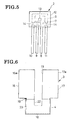
- the Hall generator assembly 2 is shown by itself in FIG. 5, and the current-path conductor 3 with the magnetic overlay 4 thereon in FIG. 6.
- the Hall generator assembly 2 and the current-path conductor 3 are put together as in FIGS. 1-3 at a final stage of manufacture of this current detector.
- the current detector 1 further includes a casing 5, FIGS.
- the first illustrated current detector 1 will be set forth more specifically hereinbelow under the headings of "Hall Generator Assembly,” “Current-Path Conductor” and “Magnetic Overlay.” Operational description will be given following the explanation of the listed three components.
- the Hall generator assembly 2 is, in essence, an integrated Hall generator circuit including a semiconductor substrate 6 overlying a baseplate 7, as best revealed in FIG. 3. Additional components of the Hall generator assembly 2 include a set of leads 8, 9, 10 and 11 for connection of this current detector to external circuitry, and a plastic encapsulation 12 enveloping all the listed components of the Hall generator assembly but most parts of the leads 8-11.
- the Hall generator assembly 2 has a Hall-effect device or Hall generator 13 formed in the semiconductor substrate 6 for generating a Hall voltage proportional to the magnitude of the current flowing through the current path conductor 3.
- the substrate 6 is of any known or suitable semiconductor material such as gallium arsenide.
- This substrate has additionally formed therein an amplifier 31, a control current supply circuit 32, and four terminals 33, 34, 35 and 36.
- the construction of this semiconductor chip is generally conventional, so that no more detailed illustration of the amplifier 31 and the control current supply circuit 32 is considered necessary; only, the Hall generator 13 is shown in further detail in FIGS. 8 and 9 as it bears more or less direct pertinence to the improvements that are introduced into this current detector by the instant invention.
- the Hall generator 13 is constituted of five n -type semiconductor regions 41, 42, 43, 44 and 45 and three p -type semiconductor regions 46, 47 and 48, which are all formed in the substrate 6 of rectangular shape as seen in a plan view as in FIG. 7.
- the fifth n -type semiconductor region 45 is formed as an island, which is cross-shaped as seen in a plan view as in FIG. 8, in the third p -type semiconductor region 48 which occupies most part of the substrate 6.
- the first and second n -type semiconductor regions 41 and 42 are both formed as islands in the region 45 with a spacing therebetween along the y -axis indicated in FIG. 8.
- electrodes 49 and 50 are in ohmic contact respectively with the first and second n -type semiconductor regions 41 and 42.
- the electrodes 49 and 50 are both connected to the control current supply circuit 32 in order to cause control current I c , FIG. 8, to flow through the fifth n -type semiconductor region 45 from the first n -type semiconductor region 41 to the second n -type semiconductor region 42. It is understood that the electrodes 49 and 50 are electrically connected via the control current supply circuit 32 to the pair of terminals 35 and 36, FIG. 7, thereby to be coupled to a direct current power supply, not shown.
- the third and fourth n -type semiconductor regions 43 and 44 are formed adjacent the center of the fifth n -type semiconductor region in the direction of the y -axis and spaced from each other in the direction of the x -axis for detection of the Hall voltage. These regions 43 and 44 are partly contiguous to the fifth n -type semiconductor region 45 and partly to the first and second p -type semiconductor regions 46 and 47. These p -type semiconductor regions 46 and 47 are intended to limit the areas of contact of the third and fourth n -type semiconductor regions 43 and 44 with the fifth n -type semiconductor region 45.
- FIGS. 7 and 9 indicate that electrodes 51 and 52 are in ohmic contact with the third and fourth n -type semiconductor regions 43 and 44. The electrodes 51 and 52 are electrically coupled to the terminals 33 and 34, respectively, via the amplifier 31.
- a Hall voltage will develop between the third and fourth n -type semiconductor regions 43 and 44 in proportion to the strength of the magnetic field applied normal to the flow of the control current I c from the first n -type semiconductor region 41 to the second n -type semiconductor region 42 as in FIG. 8.
- the part of the fifth n -type semiconductor region 45 which lies between the first and second n -type semiconductor regions 41 and 42 and between the third and fourth n -type semiconductor regions 43 and 44 constitutes the primary working part of the Hall generator 13 where the Hall voltage is generated, in the narrower sense of the term.
- this term may be construed to refer to the entire fifth n -type semiconductor region 45.
- FIG. 9 best indicates that the semiconductor substrate 6 has an insulating layer 53, as of silicon oxide, formed on one major surface thereof and a metallic layer 54, as of aluminum, on the other major surface thereof.
- the insulating layer 53 takes the form of a lamination of two sublayers 53 a and 53 b for convenience in wiring.
- the electrodes 49 and 50, FIG. 7, are coupled to the first and second n -type semiconductor regions 41 and 42, respectively, via openings in these insulating sublayers 53 a and 53 b .
- the electrodes 51 and 52, FIG. 7, are coupled to the third and fourth n -type semiconductor regions 43 and 44, respectively, via openings in the insulating sublayer 53 a .
- the metallic layer 54 on the other major surface of the substrate 6 is bonded at 55 to the mounting plate 7 shown also in FIG. 3.
- the bonding agent 55 may be either electrically conductive or insulating.
- FIG. 5 best indicates that the mounting plate 7 is generally rectangular in shape, with an area greater than that of the semiconductor substrate 6.
- the mounting plate 7 and the four leads 8-11 are punchings made from the same sheet metal material such as sheet copper with a nickel plating.
- the mounting plate 7 is joined directly to the lead 8 and electrically coupled to the terminal 33, FIG. 7.
- the other leads 9-11 are connected to the terminals 34-36 via the wires 14, respectively.
- the leads 8 and 9 are for putting out the Hall voltage, and the leads 10 and 11 for supplying the control current I c to the Hall generator 13.
- the current-path conductor 3 provides the path for the current to be detected by the Hall generator assembly 2.
- the current-path conductor 3 is a punching of sheet copper, complete with a nickel plating, that is sufficiently thick to carry current of, say, 100 amperes or so.
- the current-path conductor 3 is generally U-shaped in this particular embodiment as a relatively wide and deep slit 15 is cut therein, providing a pair of limbs 16 and 17 extending in parallel spaced relationship to each other, and a bight 18 joining the limbs each at one end thereof.
- the conductor limbs 16 and 17 are formed to include terminal portions 16 a and 17 a which are to be coupled to the electric circuit, not shown, to be tested.
- the reference numeral 19 generally denotes the midsection of the current-path conductor 3 which is constituted of the bight 18 and the immediately adjoining parts of the limbs 16 and 17. It is this short-U-shaped midsection 19 of the current-path conductor 3 that creates the magnetic field to act on the Hall generator 13.
- FIG. 1 clearly indicates that, as seen in a direction normal to the plane of the sheet-metal current-path conductor 3, the Hall generator 13 is considerably less in size than, and so is wholly contained in, the space bounded by the midsection 19 of the current-path conductor.
- the short-U-shaped midsection 19 of the current-path conductor 3 has a pair of opposite major surfaces 20 and 21, a set of three inside surfaces 22, and a set of three outside surfaces 23.
- the inside surfaces 22 bound the deepest part of the slit 15. Both inside surfaces 22 and outside surfaces 23 are at right angles with the major surfaces 20 and 21.
- the magnetic overlay 4 on the current-path conductor 3 appears in FIGS. 1-4 and 5. It is clear from these figures that the magnetic overlay 4 covers one major surface 21, facing away from the Hall generator assembly 2, and outside surfaces 23 of the current-path conductor midsection 19.
- the magnetic overlay 4 is a sheet or film of magnetic material, preferably Permalloy (tradename for a series of highly magnetically permeable iron-base alloys containing approximately 35-80% nickel).
- the magnetic overlay 4 has a specific magnetic permeability of 5500, which is higher than that of the ambient air or of the casing 5, and a thickness of 100 microns, which is less than that of the current-path conductor 3.
- the Permalloy overlay 4 can plated on the required surfaces of the current-path conductor midsection 19. Alternatively, however, such an overlay may be created either by bonding, as with an epoxy adhesive, of a preformed sheet or film, by vaporization, pressure welding, or deposition, or by any other known or suitable method.
- the current-path conductor 3 is combined with the Hall generator assembly 2 by holding the plastic encapsulation 12 of the Hall generator assembly 2 against the major surface 20, left uncovered by the magnetic overlay 4, of the current path conductor midsection 19 as in FIGS. 2 and 3.
- the relative placement of the Hall generator assembly 2 and the current-path conductor 3 must be such that, as seen in a plan view as in FIG. 1, the Hall generator 13 is wholly contained as aforesaid inside the U-shaped midsection of the current-path conductor. This placement is necessary that the magnetic lines of force created upon current flow through the current-path conductor 3 may act at least in part perpendicular to the surface of the Hall generator 13.
- the Hall generator assembly 2 and the current-path conductor 3 with the magnetic overlay 4 thereon are both partly enveloped by the casing 5 of epoxy resin or like electrically insulating material molded in place thereon.
- the pair of terminals 16 a and 17 a of the current-path conductor 3, and most parts of the leads 8-11 are left projecting from the casing 5.
- the pair of terminals 16 a and 17 a of the current-path conductor 3 may be connected to the electric circuit to be tested, so that the current to be detected or measured may flow through the U-shaped path of the conductor. Let it be assumed that the current flows from terminal 17 a to terminal 16 a .
- the current flow will create magnetic lines of force in a clockwise direction, as seen in FIG. 3, around the current-path conductor limb 16 and in a counterclockwise direction around the other limb 17. These magnetic lines will therefore act on the Hall generator 13 in the same direction.
- the magnetic overlay 4 is designed exactly to this end. As will be recalled by reference to FIG. 3, the magnetic overlay 4 covers the major surface 21 and outer surfaces 23, which are both relatively far, and are directed away, from the Hall generator 13, but not the other major surface 20 and the inside surfaces 22, which are both closer to, and are directed toward, the Hall generator. Being higher in magnetic permeability than air and the casing 5, the magnetic overlay 4 functions as a low resistance path for the magnetic flux, preventing the magnetic lines from dispersion and so keeping the flux density higher than if it were not provided.
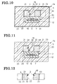
- This second preferred form of current detector 1 a features a second magnetic overlay 31 and a third magnetic overlay 32 in addition to the first magnetic overlay 4 covering part of the current-path conductor 3 as in the FIGS. 1-9 current detector 1.
- the second magnetic overlay 31 overlies one major surface of the baseplate 7, and the semiconductor chip 6 including the Hall generator and associated electronics is mounted to this baseplate via the second magnetic overlay 31.
- the third magnetic overlay 32 covers the complete surfaces of the insulating casing 5 except where it might contact the pair of terminal portions 16 a and 17 a , FIG. 1, of the current-path conductor 3 and the set of leads 8-11.
- both second and third magnetic overlays 31 and 32 may be of Permalloy with a specific magnetic permeability of 5500 and a thickness of 100 microns. Such overlays may be either bonded to the required surfaces or may be created in place thereon by any available methods. The additional magnetic overlays 31 and 32 will serve further to heighten the sensitivity of the current detector by lessen the dispersion of the magnetic lines.
- FIG. 11 current detector 1 b differs from the foregoing devices 1 and 1 a in having a magnetic overlay 4 a covering only the major surface 21, which faces away from the Hall generator assembly 2, of the short-U-shaped midsection 19 of the current-path conductor 3. All the other details of construction are as set forth above in connection with the FIGS. 1-9 current detector 1.
- the magnetic overlay 4 a has proved to work for higher sensitivity by limiting the dispersion of the magnetic lines in a direction away from the Hall generator assembly 2.
- the current-path conductor midsection 19 may have only its outer surfaces 23 covered with a magnetic overlay, as indicated at 4 b in FIG. 12. Such an overlay 4 b will also lead to some appreciable improvement in sensitivity as it restricts outward spreading of the magnetic lines.
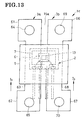
- FIG. 13 a further preferred form of current detector 1 c according to the invention which is adapted for detection of current leakage, among other purposes.
- the current detector 1 c has a pair of elongate sheet-metal current-path conductors 3 a and 3 b in place of the unitary U-shaped current-path conductor 3 of the FIGS. 1-9 current detector 1.
- the pair of current-path conductors 3 a and 3 b are combined by an epoxy casing 5 with the Hall generator assembly 2 of the same construction as in FIGS. 1-9. Encircling parts of the current-path conductors 3 a and 3 b and most part of the Hall generator assembly 2, the epoxy casing 5 rigidly holds the current-path conductors in prescribed positional relationship to each other and to the Hall generator 13.
- the pair of current-path conductors 3 a and 3 b are held by the casing 5, not shown here, parallel to each other with a spacing 15 a therebetween.
- This spacing may be considered functionally equivalent to the slit 15 of the FIGS. 1-9 current-path conductor 3, as the Hall generator 13 is wholly contained in this space as seen in a plan view as in FIG. 14.
- the current-path conductor 3 a has a pair of terminal sections 61 and 62, with connection holes 64 and 65 cut centrally therein, and a midsection 63 between the terminal sections.
- the other current-path conductor 3 b likewise comprises a pair of terminal sections 66 and 67, with connection holes 69 and 70 cut centrally therein, and a midsection 68 between these terminal sections.
- the current-path conductor midsections 63 and 68 are partly covered with overlays 71 and 72, respectively, of Permalloy or like magnetic material.
- FIG. 15 which is a section taken along XV-XV in FIG. 14, the magnetic overlays 71 and 72 are in essentially the same positional relationship to the Hall generator 13.
- the magnetic overlay 71 covers only those two surfaces of the current-path conductor midsection 63, which is rectangular in cross sectional shape, which face away from the Hall generator 13.
- the other magnetic overlay 72 covers only those two surfaces of the current-path conductor midsection 68 of similar cross sectional shape which face away from the Hall generator 13.
- the current detector 1 c offers the same advantages as does the FIGS. 1-9 device 1.
- the pair of current-path conductors 3 a and 3 b may be serially connected respectively to the pair of power conductors to be tested, not shown, in such a way that the currents I a and I b may flow in the same direction through the conductors 3 a and 3 b , as indicated by the arrows in FIG. 13.
- the currents I a and I b will be of the same magnitude if there is no leakage.
- the Hall generator 35 will produce no voltage when the currents I a and I b are of the same magnitude, since the magnetic fluxes due to the currents I a and I b act on the Hall generator in opposite directions. In event a current leakage does occur, however, the currents I a and I b will be unequal in magnitude, so that the Hall generator 35 will put out a voltage in proportion with the magnitude of the leaking current.
- FIGS. 13-15 embodiment lends itself to use as a current balance detector as well.
- the Hall voltage proportional to the difference between the magnitudes of two currents to be measured will be produced as such currents are made to flow through the pair of current path conductors 3 a and 3 b .
- the FIGS. 13-15 current detector 1 c is readily adaptable for use in the same manner as the FIGS. 1-9 device 1 as the pair of current-path conductors 3 a and 3 b provide the U-shaped current path as its terminal sections 62 and 67, for instance, are electrically interconnected.
Landscapes
- Physics & Mathematics (AREA)
- General Physics & Mathematics (AREA)
- Measuring Instrument Details And Bridges, And Automatic Balancing Devices (AREA)
- Measurement Of Current Or Voltage (AREA)
- Hall/Mr Elements (AREA)
Abstract
Description
Claims (12)
- A current detector utilizing the Hall-effect for detection or measurement of electric current, comprising a current-path conductor (3; or 3 a and 3 b ) for carrying current to be detected or measured, and a Hall generator (13) disposed in prescribed positional relationship to the current-path conductor for generating a Hall voltage proportional to the strength of a magnetic field due to the current flowing through the current-path conductor, characterized in that a magnetic overlay (4 or 4 a or 4 b ; or 71 and 72) in the form of a sheet or film of magnetic material covers part of the current-path conductor (3; or 3 a and 3 b ) for a higher sensitivity of current detection through enhancement of flux density acting on the Hall generator.
- A current detector as claimed in claim 1, wherein the current-path conductor (3; or 3 a and 3 b ) is formed to include a pair of opposite terminal portions (16 a and 17 a ; or 61 and 62, and 66 and 67) and a midsection (19; or 63 and 68) therebetween, and wherein the Hall generator (13) is so positioned relative to the current-path conductor as to be acted upon by a magnetic field due to the current flowing through the midsection of the current-path conductor, characterized in that the magnetic overlay (4 or 4 a or 4 b ; or 71 and 72) covers at least part of the midsection of the current-path conductor.
- A current detector as claimed in claim 2, wherein the midsection (19) of the current-path conductor (3) extends around the Hall generator (13) in a plane not containing the Hall generator, and wherein the midsection of the current-path conductor is rectangular in cross sectional shape, having a first major surface (20) directed toward the Hall generator, a second major surface (21) directed away from the Hall generator, an inside surface (22) directed toward the Hall generator, and an outside surface (23) directed away from the Hall generator, characterized in that the magnetic overlay (4 a ) covers the second major surface (21) of the current-path conductor.
- A current detector as claimed in claim 2, wherein the midsection (19) of the current-path conductor (3) extends around the Hall generator (13) in a plane not containing the Hall generator, and wherein the midsection of the current-path conductor is rectangular in cross sectional shape, having a first major surface (20) directed toward the Hall generator, a second major surface (21) directed away from the Hall generator, an inside surface (22) directed toward the Hall generator, and an outside surface (23) directed away from the Hall generator, characterized in that the magnetic overlay (4 b ) covers the outside surface (23) of the current-path conductor.
- A current detector as claimed in claim 2, wherein the midsection (19) of the current-path conductor (3) extends around the Hall generator (13) in a plane not containing the Hall generator, and wherein the midsection of the current-path conductor is rectangular in cross sectional shape, having a first major surface (20) directed toward the Hall generator, a second major surface (21) directed away from the Hall generator, an inside surface (22) directed toward the Hall generator, and an outside surface (23) directed away from the Hall generator, characterized in that the magnetic overlay (4) covers both second major surface (20) and outside surface (23) of the current-path conductor.
- A current detector as claimed in claim 2, wherein the Hall generator (13) is formed in a semiconductor substrate (6) having a first major surface directed toward the current-path conductor (3), and a second major surface directed away from the current-path conductor, characterized in that the current detector has a second magnetic overlay (31) held against the second major surface of the semiconductor substrate.
- A current detector as claimed in claim 1, wherein the Hall generator (13) and at least part of the current-path conductor (3) with the magnetic overlay (4) thereon are enveloped by a casing (5) of electrically insulating material, characterized in that at least part of the casing is covered by a second magnetic overlay (32).
- A current detector as claimed in claim 1, characterized in that the magnetic overlay (4, 4 a , 4 b ; 71, 72) is of Permalloy.
- A current detector utilizing the Hall-effect for detection or measurement of electric current, comprising a current-path conductor (3) in the form of a piece of sheet metal having a slit (15) cut therein for providing a U-shaped path for the flow of current to be detected or measured, the sheet-metal current-path conductor having a pair of opposite major surfaces (20, 21), an inside surface (22) contiguous to the slit, and an outside surface (23) facing away from the slit, a Hall generator (13) for generating a Hall voltage proportional to the strength of an applied magnetic field, and an encapsulation (12) of electrically insulating material integrally enveloping the Hall generator and held against one (20) of the major surfaces of the current-path conductor, with the Hall generator positioned inside the slit (15) therein, as seen in a direction normal to the sheet-metal current-path conductor, for generating a Hall voltage indicative of the magnitude of the current flowing through the U-shaped current path, characterized in that a magnetic overlay (4, 4 a , or 4 b ) in the form of a sheet or film of magnetic material covers at least either of the other major surface (21) and outside surface (23) of the current-path conductor (3) for a higher sensitivity of current detection through enhancement of flux density acting on the Hall generator (13).
- A current detector as claimed in claim 9, wherein the Hall generator (13) is formed in a semiconductor substrate (6) overlying a baseplate (7), characterized in that a second magnetic overlay (31) is formed on the baseplate (7).
- A current detector as claimed in claim 9, wherein the encapsulation (12), together with the Hall generator (13) therein, and at least part of the current-path conductor (3) together with the magnetic overlay (4) thereon are enveloped by a casing (5) of electrically insulating material, characterized in that at least part of the casing (5) is covered by a second magnetic overlay (32).
- A current detector utilizing the Hall-effect for detection or measurement of electric current, comprising a pair of current-path conductors (3 a and 3 b ) each in the form of an elongate piece of sheet metal for carrying current to be detected or measured, the pair of current-path conductors extending in parallel spaced, coplanar relationship to each other, each sheet-metal current-path conductor having a pair of opposite major surfaces, an inside surface directed toward the other current-path conductor, and an outside surface directed away from the other current-path conductor, a Hall generator (13) for generating a Hall voltage proportional to a difference between the magnitudes of currents flowing through the respective current-path conductors, a casing (5) of electrically insulating material holding the Hall generator opposite the pair of current-path conductors and inside the space therebetween, as seen in a direction normal to the plane of the sheet-metal current-path conductors, the Hall generator being directed toward one of the major surfaces of each current-path conductor, and a magnetic overlay (71, 72) in the form of a sheet or film of magnetic material covering at least either of the other major surface and outside surface of each current-path conductor (3 a or 3 b ) for a higher sensitivity of current detection through enhancement of flux density acting on the Hall generator.
Applications Claiming Priority (2)
| Application Number | Priority Date | Filing Date | Title |
|---|---|---|---|
| JP2001206175A JP4164629B2 (en) | 2000-10-23 | 2001-07-06 | Current detection device with Hall element |
| JP2001206175 | 2001-07-06 |
Publications (3)
| Publication Number | Publication Date |
|---|---|
| EP1281974A2 true EP1281974A2 (en) | 2003-02-05 |
| EP1281974A3 EP1281974A3 (en) | 2003-08-27 |
| EP1281974B1 EP1281974B1 (en) | 2007-04-18 |
Family
ID=19042350
Family Applications (1)
| Application Number | Title | Priority Date | Filing Date |
|---|---|---|---|
| EP02014368A Expired - Lifetime EP1281974B1 (en) | 2001-07-06 | 2002-06-27 | Hall-effect current detector |
Country Status (3)
| Country | Link |
|---|---|
| US (1) | US6727683B2 (en) |
| EP (1) | EP1281974B1 (en) |
| DE (1) | DE60219561T2 (en) |
Cited By (11)
| Publication number | Priority date | Publication date | Assignee | Title |
|---|---|---|---|---|
| EP2295993A1 (en) * | 2005-05-27 | 2011-03-16 | Allegro Microsystems Inc. | Current Sensor |
| US8080994B2 (en) | 2006-05-12 | 2011-12-20 | Allegro Microsystems, Inc. | Integrated current sensor |
| US8629539B2 (en) | 2012-01-16 | 2014-01-14 | Allegro Microsystems, Llc | Methods and apparatus for magnetic sensor having non-conductive die paddle |
| US9190606B2 (en) | 2013-03-15 | 2015-11-17 | Allegro Micosystems, LLC | Packaging for an electronic device |
| US9666788B2 (en) | 2012-03-20 | 2017-05-30 | Allegro Microsystems, Llc | Integrated circuit package having a split lead frame |
| US9812588B2 (en) | 2012-03-20 | 2017-11-07 | Allegro Microsystems, Llc | Magnetic field sensor integrated circuit with integral ferromagnetic material |
| US10234513B2 (en) | 2012-03-20 | 2019-03-19 | Allegro Microsystems, Llc | Magnetic field sensor integrated circuit with integral ferromagnetic material |
| US10345343B2 (en) | 2013-03-15 | 2019-07-09 | Allegro Microsystems, Llc | Current sensor isolation |
| US10991644B2 (en) | 2019-08-22 | 2021-04-27 | Allegro Microsystems, Llc | Integrated circuit package having a low profile |
| US11768230B1 (en) | 2022-03-30 | 2023-09-26 | Allegro Microsystems, Llc | Current sensor integrated circuit with a dual gauge lead frame |
| US11800813B2 (en) | 2020-05-29 | 2023-10-24 | Allegro Microsystems, Llc | High isolation current sensor |
Families Citing this family (34)
| Publication number | Priority date | Publication date | Assignee | Title |
|---|---|---|---|---|
| US7075287B1 (en) | 2003-08-26 | 2006-07-11 | Allegro Microsystems, Inc. | Current sensor |
| US6995315B2 (en) * | 2003-08-26 | 2006-02-07 | Allegro Microsystems, Inc. | Current sensor |
| US7166807B2 (en) | 2003-08-26 | 2007-01-23 | Allegro Microsystems, Inc. | Current sensor |
| US7709754B2 (en) * | 2003-08-26 | 2010-05-04 | Allegro Microsystems, Inc. | Current sensor |
| US7476816B2 (en) * | 2003-08-26 | 2009-01-13 | Allegro Microsystems, Inc. | Current sensor |
| JP4224483B2 (en) * | 2005-10-14 | 2009-02-12 | Tdk株式会社 | Current sensor |
| US7612553B2 (en) * | 2007-07-26 | 2009-11-03 | Honeywell International Inc. | Current sensor having sandwiched magnetic permeability layer |
| WO2009055709A1 (en) * | 2007-10-24 | 2009-04-30 | Gerald Givens | Power line sensor |
| US8477027B2 (en) * | 2007-10-24 | 2013-07-02 | Gerald E. Givens | Wireless sensor system |
| US8093670B2 (en) * | 2008-07-24 | 2012-01-10 | Allegro Microsystems, Inc. | Methods and apparatus for integrated circuit having on chip capacitor with eddy current reductions |
| US9222992B2 (en) * | 2008-12-18 | 2015-12-29 | Infineon Technologies Ag | Magnetic field current sensors |
| DE102009028956A1 (en) * | 2009-08-28 | 2011-03-03 | Robert Bosch Gmbh | magnetic field sensor |
| US8717016B2 (en) | 2010-02-24 | 2014-05-06 | Infineon Technologies Ag | Current sensors and methods |
| US8760149B2 (en) * | 2010-04-08 | 2014-06-24 | Infineon Technologies Ag | Magnetic field current sensors |
| US8680843B2 (en) | 2010-06-10 | 2014-03-25 | Infineon Technologies Ag | Magnetic field current sensors |
| US8283742B2 (en) | 2010-08-31 | 2012-10-09 | Infineon Technologies, A.G. | Thin-wafer current sensors |
| US9476915B2 (en) | 2010-12-09 | 2016-10-25 | Infineon Technologies Ag | Magnetic field current sensors |
| US8975889B2 (en) | 2011-01-24 | 2015-03-10 | Infineon Technologies Ag | Current difference sensors, systems and methods |
| US8963536B2 (en) | 2011-04-14 | 2015-02-24 | Infineon Technologies Ag | Current sensors, systems and methods for sensing current in a conductor |
| US8907437B2 (en) | 2011-07-22 | 2014-12-09 | Allegro Microsystems, Llc | Reinforced isolation for current sensor with magnetic field transducer |
| US9494660B2 (en) | 2012-03-20 | 2016-11-15 | Allegro Microsystems, Llc | Integrated circuit package having a split lead frame |
| USD684927S1 (en) * | 2012-05-16 | 2013-06-25 | Lem Intellectual Property Sa | Current transducer |
| USD685734S1 (en) * | 2012-05-16 | 2013-07-09 | Lem Intellectual Property Sa | Current transducer |
| USD688626S1 (en) * | 2012-05-16 | 2013-08-27 | Lem Intellectual Property Sa | Current transducer |
| USD686156S1 (en) * | 2012-05-16 | 2013-07-16 | Lem Intellectual Property Sa | Current transducer |
| USD685325S1 (en) * | 2012-05-16 | 2013-07-02 | Lem Intellectual Property Sa | Current transducer |
| USD686989S1 (en) * | 2012-05-16 | 2013-07-30 | Lem Intellectual Property Sa | Current transducer |
| US9411025B2 (en) | 2013-04-26 | 2016-08-09 | Allegro Microsystems, Llc | Integrated circuit package having a split lead frame and a magnet |
| US10505102B2 (en) * | 2016-04-04 | 2019-12-10 | Infineon Technologies Ag | Semiconductor device for sensing a magnetic field including an encapsulation material defining a through-hole |
| CN114008464A (en) * | 2019-08-26 | 2022-02-01 | 株式会社村田制作所 | Current sensor |
| US11320466B1 (en) | 2020-10-29 | 2022-05-03 | Allegro Microsystems, Llc | Differential current sensor |
| US11402409B1 (en) | 2021-03-22 | 2022-08-02 | Allegro Microsystems, Llc | Differential current sensor package |
| US11644485B2 (en) | 2021-10-07 | 2023-05-09 | Allegro Microsystems, Llc | Current sensor integrated circuits |
| EP4435437A1 (en) * | 2023-03-20 | 2024-09-25 | LEM International SA | Current transducer for measuring residual currents |
Family Cites Families (10)
| Publication number | Priority date | Publication date | Assignee | Title |
|---|---|---|---|---|
| US4059798A (en) * | 1976-03-08 | 1977-11-22 | F. W. Bell, Inc. | Method and apparatus for measuring the current flowing in a workpiece |
| US4639665A (en) * | 1983-08-22 | 1987-01-27 | Borg-Warner Corporation | Sensing system for measuring a parameter |
| US4823075A (en) * | 1987-10-13 | 1989-04-18 | General Electric Company | Current sensor using hall-effect device with feedback |
| JPH04364472A (en) | 1991-06-12 | 1992-12-16 | Fuji Electric Co Ltd | Magnetoelectric conversion device |
| JPH07239347A (en) * | 1994-02-28 | 1995-09-12 | Nippondenso Co Ltd | Current-measuring apparatus of magnetic balance type |
| EP0772046B1 (en) * | 1995-10-30 | 2002-04-17 | Sentron Ag | Magnetic field probe and current or energy probe |
| DE19650078A1 (en) * | 1996-12-03 | 1998-06-04 | Inst Mikrostrukturtechnologie | Sensor element for determining magnetic field or current |
| DE19819470B4 (en) * | 1998-01-08 | 2011-06-09 | Lust Antriebstechnik Gmbh | Method for the potential-free measurement of currents by the recording of the magnetic field caused by them and devices for carrying out the method |
| US6426617B1 (en) * | 1999-09-28 | 2002-07-30 | Rockwell Automation Technologies, Inc. | Hall effect current sensor system packaging |
| JP2001165963A (en) * | 1999-12-09 | 2001-06-22 | Sanken Electric Co Ltd | Current detection device with Hall element |
-
2002
- 2002-06-27 EP EP02014368A patent/EP1281974B1/en not_active Expired - Lifetime
- 2002-06-27 DE DE60219561T patent/DE60219561T2/en not_active Expired - Fee Related
- 2002-07-02 US US10/188,693 patent/US6727683B2/en not_active Expired - Fee Related
Cited By (21)
| Publication number | Priority date | Publication date | Assignee | Title |
|---|---|---|---|---|
| EP2295993A1 (en) * | 2005-05-27 | 2011-03-16 | Allegro Microsystems Inc. | Current Sensor |
| US8080994B2 (en) | 2006-05-12 | 2011-12-20 | Allegro Microsystems, Inc. | Integrated current sensor |
| US8629539B2 (en) | 2012-01-16 | 2014-01-14 | Allegro Microsystems, Llc | Methods and apparatus for magnetic sensor having non-conductive die paddle |
| US10333055B2 (en) | 2012-01-16 | 2019-06-25 | Allegro Microsystems, Llc | Methods for magnetic sensor having non-conductive die paddle |
| US9620705B2 (en) | 2012-01-16 | 2017-04-11 | Allegro Microsystems, Llc | Methods and apparatus for magnetic sensor having non-conductive die paddle |
| US9666788B2 (en) | 2012-03-20 | 2017-05-30 | Allegro Microsystems, Llc | Integrated circuit package having a split lead frame |
| US11444209B2 (en) | 2012-03-20 | 2022-09-13 | Allegro Microsystems, Llc | Magnetic field sensor integrated circuit with an integrated coil enclosed with a semiconductor die by a mold material |
| US11961920B2 (en) | 2012-03-20 | 2024-04-16 | Allegro Microsystems, Llc | Integrated circuit package with magnet having a channel |
| US10230006B2 (en) | 2012-03-20 | 2019-03-12 | Allegro Microsystems, Llc | Magnetic field sensor integrated circuit with an electromagnetic suppressor |
| US10234513B2 (en) | 2012-03-20 | 2019-03-19 | Allegro Microsystems, Llc | Magnetic field sensor integrated circuit with integral ferromagnetic material |
| US11828819B2 (en) | 2012-03-20 | 2023-11-28 | Allegro Microsystems, Llc | Magnetic field sensor integrated circuit with integral ferromagnetic material |
| US11677032B2 (en) | 2012-03-20 | 2023-06-13 | Allegro Microsystems, Llc | Sensor integrated circuit with integrated coil and element in central region of mold material |
| US9812588B2 (en) | 2012-03-20 | 2017-11-07 | Allegro Microsystems, Llc | Magnetic field sensor integrated circuit with integral ferromagnetic material |
| US10916665B2 (en) | 2012-03-20 | 2021-02-09 | Allegro Microsystems, Llc | Magnetic field sensor integrated circuit with an integrated coil |
| US10753963B2 (en) | 2013-03-15 | 2020-08-25 | Allegro Microsystems, Llc | Current sensor isolation |
| US10345343B2 (en) | 2013-03-15 | 2019-07-09 | Allegro Microsystems, Llc | Current sensor isolation |
| US9190606B2 (en) | 2013-03-15 | 2015-11-17 | Allegro Micosystems, LLC | Packaging for an electronic device |
| US9865807B2 (en) | 2013-03-15 | 2018-01-09 | Allegro Microsystems, Llc | Packaging for an electronic device |
| US10991644B2 (en) | 2019-08-22 | 2021-04-27 | Allegro Microsystems, Llc | Integrated circuit package having a low profile |
| US11800813B2 (en) | 2020-05-29 | 2023-10-24 | Allegro Microsystems, Llc | High isolation current sensor |
| US11768230B1 (en) | 2022-03-30 | 2023-09-26 | Allegro Microsystems, Llc | Current sensor integrated circuit with a dual gauge lead frame |
Also Published As
| Publication number | Publication date |
|---|---|
| DE60219561D1 (en) | 2007-05-31 |
| DE60219561T2 (en) | 2008-01-03 |
| EP1281974B1 (en) | 2007-04-18 |
| US20030006752A1 (en) | 2003-01-09 |
| EP1281974A3 (en) | 2003-08-27 |
| US6727683B2 (en) | 2004-04-27 |
Similar Documents
| Publication | Publication Date | Title |
|---|---|---|
| US6727683B2 (en) | Hall-effect current detector | |
| US6759841B2 (en) | Hall-effect current detector | |
| US6545457B2 (en) | Current detector utilizing hall effect | |
| US6841989B2 (en) | Hall-effect current detector | |
| US6781358B2 (en) | Hall-effect current detector | |
| US6769166B1 (en) | Method of making an electrical current sensor | |
| JP4757195B2 (en) | Current sensor | |
| US6462531B1 (en) | Current detector having a hall-effect device | |
| US6812687B1 (en) | Semiconductor current detector of improved noise immunity | |
| JP4164629B2 (en) | Current detection device with Hall element | |
| US7782049B2 (en) | Magnetic device | |
| JP2001339109A (en) | Current detection device equipped with a ball element | |
| WO2006083479A1 (en) | Integrated sensor having a magnetic flux concentrator | |
| JP2002202327A (en) | Current detector equipped with hall element | |
| JP3230580B2 (en) | Current detection device equipped with a ball element | |
| JP4507599B2 (en) | Current detector | |
| JP2003215171A (en) | Current detector provided with hall element | |
| JP2003098195A (en) | Current detector | |
| JP2005147755A (en) | Current detector | |
| JPH09243667A (en) | Current detector | |
| CN118522722A (en) | Chip packaging structure with anti-magnetic interference | |
| JP2001177309A5 (en) | ||
| JPH07220918A (en) | Stop-pin magnet for stopping rotation of magnetic flux | |
| JP2017120203A (en) | Magnetic sensor module |
Legal Events
| Date | Code | Title | Description |
|---|---|---|---|
| PUAI | Public reference made under article 153(3) epc to a published international application that has entered the european phase |
Free format text: ORIGINAL CODE: 0009012 |
|
| AK | Designated contracting states |
Designated state(s): AT BE CH CY DE DK ES FI FR GB GR IE IT LI LU MC NL PT SE TR |
|
| AX | Request for extension of the european patent |
Extension state: AL LT LV MK RO SI |
|
| PUAL | Search report despatched |
Free format text: ORIGINAL CODE: 0009013 |
|
| AK | Designated contracting states |
Designated state(s): AT BE CH CY DE DK ES FI FR GB GR IE IT LI LU MC NL PT SE TR |
|
| AX | Request for extension of the european patent |
Extension state: AL LT LV MK RO SI |
|
| 17P | Request for examination filed |
Effective date: 20031023 |
|
| AKX | Designation fees paid |
Designated state(s): DE FR NL |
|
| 17Q | First examination report despatched |
Effective date: 20040507 |
|
| GRAP | Despatch of communication of intention to grant a patent |
Free format text: ORIGINAL CODE: EPIDOSNIGR1 |
|
| GRAS | Grant fee paid |
Free format text: ORIGINAL CODE: EPIDOSNIGR3 |
|
| GRAA | (expected) grant |
Free format text: ORIGINAL CODE: 0009210 |
|
| AK | Designated contracting states |
Kind code of ref document: B1 Designated state(s): DE FR NL |
|
| REF | Corresponds to: |
Ref document number: 60219561 Country of ref document: DE Date of ref document: 20070531 Kind code of ref document: P |
|
| PGFP | Annual fee paid to national office [announced via postgrant information from national office to epo] |
Ref country code: DE Payment date: 20070702 Year of fee payment: 6 |
|
| NLV1 | Nl: lapsed or annulled due to failure to fulfill the requirements of art. 29p and 29m of the patents act | ||
| EN | Fr: translation not filed | ||
| PG25 | Lapsed in a contracting state [announced via postgrant information from national office to epo] |
Ref country code: NL Free format text: LAPSE BECAUSE OF FAILURE TO SUBMIT A TRANSLATION OF THE DESCRIPTION OR TO PAY THE FEE WITHIN THE PRESCRIBED TIME-LIMIT Effective date: 20070418 |
|
| PLBE | No opposition filed within time limit |
Free format text: ORIGINAL CODE: 0009261 |
|
| STAA | Information on the status of an ep patent application or granted ep patent |
Free format text: STATUS: NO OPPOSITION FILED WITHIN TIME LIMIT |
|
| 26N | No opposition filed |
Effective date: 20080121 |
|
| PG25 | Lapsed in a contracting state [announced via postgrant information from national office to epo] |
Ref country code: FR Free format text: LAPSE BECAUSE OF FAILURE TO SUBMIT A TRANSLATION OF THE DESCRIPTION OR TO PAY THE FEE WITHIN THE PRESCRIBED TIME-LIMIT Effective date: 20071214 |
|
| PG25 | Lapsed in a contracting state [announced via postgrant information from national office to epo] |
Ref country code: FR Free format text: LAPSE BECAUSE OF FAILURE TO SUBMIT A TRANSLATION OF THE DESCRIPTION OR TO PAY THE FEE WITHIN THE PRESCRIBED TIME-LIMIT Effective date: 20070418 |
|
| PG25 | Lapsed in a contracting state [announced via postgrant information from national office to epo] |
Ref country code: DE Free format text: LAPSE BECAUSE OF NON-PAYMENT OF DUE FEES Effective date: 20090101 |