EP1281519A1 - Method of charging hole with fluid material - Google Patents
Method of charging hole with fluid material Download PDFInfo
- Publication number
- EP1281519A1 EP1281519A1 EP02016674A EP02016674A EP1281519A1 EP 1281519 A1 EP1281519 A1 EP 1281519A1 EP 02016674 A EP02016674 A EP 02016674A EP 02016674 A EP02016674 A EP 02016674A EP 1281519 A1 EP1281519 A1 EP 1281519A1
- Authority
- EP
- European Patent Office
- Prior art keywords
- forcing
- substrate
- fluid material
- hole
- film
- Prior art date
- Legal status (The legal status is an assumption and is not a legal conclusion. Google has not performed a legal analysis and makes no representation as to the accuracy of the status listed.)
- Granted
Links
- 239000012530 fluid Substances 0.000 title claims abstract description 36
- 239000000463 material Substances 0.000 title claims abstract description 36
- 238000000034 method Methods 0.000 title claims abstract description 26
- 239000000758 substrate Substances 0.000 claims abstract description 47
- 239000004020 conductor Substances 0.000 claims description 31
- 229920005989 resin Polymers 0.000 description 36
- 239000011347 resin Substances 0.000 description 36
- 230000001681 protective effect Effects 0.000 description 26
- 239000010410 layer Substances 0.000 description 22
- 229910000679 solder Inorganic materials 0.000 description 14
- 239000006071 cream Substances 0.000 description 8
- 238000010586 diagram Methods 0.000 description 7
- 238000007650 screen-printing Methods 0.000 description 7
- CURLTUGMZLYLDI-UHFFFAOYSA-N Carbon dioxide Chemical compound O=C=O CURLTUGMZLYLDI-UHFFFAOYSA-N 0.000 description 6
- 239000004697 Polyetherimide Substances 0.000 description 4
- 239000002184 metal Substances 0.000 description 4
- 229910052751 metal Inorganic materials 0.000 description 4
- 229920002530 polyetherether ketone Polymers 0.000 description 4
- 229920001601 polyetherimide Polymers 0.000 description 4
- 229910002092 carbon dioxide Inorganic materials 0.000 description 3
- 239000001569 carbon dioxide Substances 0.000 description 3
- 238000005553 drilling Methods 0.000 description 3
- 239000011888 foil Substances 0.000 description 3
- 239000011810 insulating material Substances 0.000 description 3
- 239000002923 metal particle Substances 0.000 description 3
- 239000002245 particle Substances 0.000 description 3
- -1 polyethylene terephthalate Polymers 0.000 description 3
- 238000007639 printing Methods 0.000 description 3
- 229920005992 thermoplastic resin Polymers 0.000 description 3
- RYGMFSIKBFXOCR-UHFFFAOYSA-N Copper Chemical compound [Cu] RYGMFSIKBFXOCR-UHFFFAOYSA-N 0.000 description 2
- 239000011230 binding agent Substances 0.000 description 2
- 238000004898 kneading Methods 0.000 description 2
- 238000004519 manufacturing process Methods 0.000 description 2
- 239000003960 organic solvent Substances 0.000 description 2
- 239000005020 polyethylene terephthalate Substances 0.000 description 2
- 229920000139 polyethylene terephthalate Polymers 0.000 description 2
- JYEUMXHLPRZUAT-UHFFFAOYSA-N 1,2,3-triazine Chemical compound C1=CN=NN=C1 JYEUMXHLPRZUAT-UHFFFAOYSA-N 0.000 description 1
- JOYRKODLDBILNP-UHFFFAOYSA-N Ethyl urethane Chemical compound CCOC(N)=O JOYRKODLDBILNP-UHFFFAOYSA-N 0.000 description 1
- 229920000106 Liquid crystal polymer Polymers 0.000 description 1
- 239000004977 Liquid-crystal polymers (LCPs) Substances 0.000 description 1
- 239000004695 Polyether sulfone Substances 0.000 description 1
- 239000004642 Polyimide Substances 0.000 description 1
- BQCADISMDOOEFD-UHFFFAOYSA-N Silver Chemical compound [Ag] BQCADISMDOOEFD-UHFFFAOYSA-N 0.000 description 1
- ATJFFYVFTNAWJD-UHFFFAOYSA-N Tin Chemical compound [Sn] ATJFFYVFTNAWJD-UHFFFAOYSA-N 0.000 description 1
- 208000027418 Wounds and injury Diseases 0.000 description 1
- 230000004913 activation Effects 0.000 description 1
- 239000012790 adhesive layer Substances 0.000 description 1
- 239000011231 conductive filler Substances 0.000 description 1
- 229910052802 copper Inorganic materials 0.000 description 1
- 239000010949 copper Substances 0.000 description 1
- 239000011889 copper foil Substances 0.000 description 1
- 230000006378 damage Effects 0.000 description 1
- 238000000151 deposition Methods 0.000 description 1
- 238000009826 distribution Methods 0.000 description 1
- 239000003822 epoxy resin Substances 0.000 description 1
- 238000005530 etching Methods 0.000 description 1
- 239000006260 foam Substances 0.000 description 1
- 208000014674 injury Diseases 0.000 description 1
- 239000000203 mixture Substances 0.000 description 1
- 238000007747 plating Methods 0.000 description 1
- 229920003207 poly(ethylene-2,6-naphthalate) Polymers 0.000 description 1
- 229920000647 polyepoxide Polymers 0.000 description 1
- 229920006393 polyether sulfone Polymers 0.000 description 1
- 239000011112 polyethylene naphthalate Substances 0.000 description 1
- 229920001721 polyimide Polymers 0.000 description 1
- 229920001955 polyphenylene ether Polymers 0.000 description 1
- 238000003825 pressing Methods 0.000 description 1
- 229910052709 silver Inorganic materials 0.000 description 1
- 239000004332 silver Substances 0.000 description 1
- 239000012815 thermoplastic material Substances 0.000 description 1
- 229920006259 thermoplastic polyimide Polymers 0.000 description 1
- 229920001187 thermosetting polymer Polymers 0.000 description 1
Images


Classifications
-
- H—ELECTRICITY
- H05—ELECTRIC TECHNIQUES NOT OTHERWISE PROVIDED FOR
- H05K—PRINTED CIRCUITS; CASINGS OR CONSTRUCTIONAL DETAILS OF ELECTRIC APPARATUS; MANUFACTURE OF ASSEMBLAGES OF ELECTRICAL COMPONENTS
- H05K3/00—Apparatus or processes for manufacturing printed circuits
- H05K3/40—Forming printed elements for providing electric connections to or between printed circuits
-
- H—ELECTRICITY
- H05—ELECTRIC TECHNIQUES NOT OTHERWISE PROVIDED FOR
- H05K—PRINTED CIRCUITS; CASINGS OR CONSTRUCTIONAL DETAILS OF ELECTRIC APPARATUS; MANUFACTURE OF ASSEMBLAGES OF ELECTRICAL COMPONENTS
- H05K3/00—Apparatus or processes for manufacturing printed circuits
- H05K3/40—Forming printed elements for providing electric connections to or between printed circuits
- H05K3/4038—Through-connections; Vertical interconnect access [VIA] connections
- H05K3/4053—Through-connections; Vertical interconnect access [VIA] connections by thick-film techniques
-
- B—PERFORMING OPERATIONS; TRANSPORTING
- B41—PRINTING; LINING MACHINES; TYPEWRITERS; STAMPS
- B41F—PRINTING MACHINES OR PRESSES
- B41F15/00—Screen printers
- B41F15/14—Details
- B41F15/40—Inking units
- B41F15/42—Inking units comprising squeegees or doctors
-
- B—PERFORMING OPERATIONS; TRANSPORTING
- B41—PRINTING; LINING MACHINES; TYPEWRITERS; STAMPS
- B41P—INDEXING SCHEME RELATING TO PRINTING, LINING MACHINES, TYPEWRITERS, AND TO STAMPS
- B41P2215/00—Screen printing machines
- B41P2215/10—Screen printing machines characterised by their constructional features
- B41P2215/13—Devices for increasing ink penetration
-
- H—ELECTRICITY
- H05—ELECTRIC TECHNIQUES NOT OTHERWISE PROVIDED FOR
- H05K—PRINTED CIRCUITS; CASINGS OR CONSTRUCTIONAL DETAILS OF ELECTRIC APPARATUS; MANUFACTURE OF ASSEMBLAGES OF ELECTRICAL COMPONENTS
- H05K2201/00—Indexing scheme relating to printed circuits covered by H05K1/00
- H05K2201/03—Conductive materials
- H05K2201/0332—Structure of the conductor
- H05K2201/0388—Other aspects of conductors
- H05K2201/0394—Conductor crossing over a hole in the substrate or a gap between two separate substrate parts
-
- H—ELECTRICITY
- H05—ELECTRIC TECHNIQUES NOT OTHERWISE PROVIDED FOR
- H05K—PRINTED CIRCUITS; CASINGS OR CONSTRUCTIONAL DETAILS OF ELECTRIC APPARATUS; MANUFACTURE OF ASSEMBLAGES OF ELECTRICAL COMPONENTS
- H05K2203/00—Indexing scheme relating to apparatus or processes for manufacturing printed circuits covered by H05K3/00
- H05K2203/01—Tools for processing; Objects used during processing
- H05K2203/0104—Tools for processing; Objects used during processing for patterning or coating
- H05K2203/0126—Dispenser, e.g. for solder paste, for supplying conductive paste for screen printing or for filling holes
-
- H—ELECTRICITY
- H05—ELECTRIC TECHNIQUES NOT OTHERWISE PROVIDED FOR
- H05K—PRINTED CIRCUITS; CASINGS OR CONSTRUCTIONAL DETAILS OF ELECTRIC APPARATUS; MANUFACTURE OF ASSEMBLAGES OF ELECTRICAL COMPONENTS
- H05K2203/00—Indexing scheme relating to apparatus or processes for manufacturing printed circuits covered by H05K3/00
- H05K2203/01—Tools for processing; Objects used during processing
- H05K2203/0191—Using tape or non-metallic foil in a process, e.g. during filling of a hole with conductive paste
-
- H—ELECTRICITY
- H05—ELECTRIC TECHNIQUES NOT OTHERWISE PROVIDED FOR
- H05K—PRINTED CIRCUITS; CASINGS OR CONSTRUCTIONAL DETAILS OF ELECTRIC APPARATUS; MANUFACTURE OF ASSEMBLAGES OF ELECTRICAL COMPONENTS
- H05K2203/00—Indexing scheme relating to apparatus or processes for manufacturing printed circuits covered by H05K3/00
- H05K2203/01—Tools for processing; Objects used during processing
- H05K2203/0195—Tool for a process not provided for in H05K3/00, e.g. tool for handling objects using suction, for deforming objects, for applying local pressure
-
- H—ELECTRICITY
- H05—ELECTRIC TECHNIQUES NOT OTHERWISE PROVIDED FOR
- H05K—PRINTED CIRCUITS; CASINGS OR CONSTRUCTIONAL DETAILS OF ELECTRIC APPARATUS; MANUFACTURE OF ASSEMBLAGES OF ELECTRICAL COMPONENTS
- H05K2203/00—Indexing scheme relating to apparatus or processes for manufacturing printed circuits covered by H05K3/00
- H05K2203/02—Details related to mechanical or acoustic processing, e.g. drilling, punching, cutting, using ultrasound
- H05K2203/0278—Flat pressure, e.g. for connecting terminals with anisotropic conductive adhesive
-
- H—ELECTRICITY
- H05—ELECTRIC TECHNIQUES NOT OTHERWISE PROVIDED FOR
- H05K—PRINTED CIRCUITS; CASINGS OR CONSTRUCTIONAL DETAILS OF ELECTRIC APPARATUS; MANUFACTURE OF ASSEMBLAGES OF ELECTRICAL COMPONENTS
- H05K3/00—Apparatus or processes for manufacturing printed circuits
- H05K3/46—Manufacturing multilayer circuits
- H05K3/4611—Manufacturing multilayer circuits by laminating two or more circuit boards
- H05K3/4614—Manufacturing multilayer circuits by laminating two or more circuit boards the electrical connections between the circuit boards being made during lamination
-
- H—ELECTRICITY
- H05—ELECTRIC TECHNIQUES NOT OTHERWISE PROVIDED FOR
- H05K—PRINTED CIRCUITS; CASINGS OR CONSTRUCTIONAL DETAILS OF ELECTRIC APPARATUS; MANUFACTURE OF ASSEMBLAGES OF ELECTRICAL COMPONENTS
- H05K3/00—Apparatus or processes for manufacturing printed circuits
- H05K3/46—Manufacturing multilayer circuits
- H05K3/4611—Manufacturing multilayer circuits by laminating two or more circuit boards
- H05K3/4614—Manufacturing multilayer circuits by laminating two or more circuit boards the electrical connections between the circuit boards being made during lamination
- H05K3/4617—Manufacturing multilayer circuits by laminating two or more circuit boards the electrical connections between the circuit boards being made during lamination characterized by laminating only or mainly similar single-sided circuit boards
Definitions
- This invention generally relates to a method of charging a hole with fluid material.
- This invention specifically relates to a method of charging a hole in a substrate with fluid material such as electrically conductive paste.
- An insulating substrate forming a printed wiring board has via holes. It is known to use screen printing to charge via holes with electrically conductive paste being a mixture of metal particles, an organic solvent, and binder resin.
- the screen printing has the following sequence of steps. First, a screen sheet is place above an insulating substrate having via holes. The screen sheet has a pattern of open areas positionally corresponding to the via holes. Electrically conductive paste is applied onto the screen sheet. Subsequently, the electrically conductive paste is transferred across the screen sheet by a squeegee while the squeegee is pressed against the screen sheet. At this time, the squeegee is moved linearly only in one direction or linearly reciprocated along two opposite directions. The squeegee forces the electrically conductive paste into the via holes through the open areas of the screen sheet.
- the screen printing tends to insufficiently charge the via holes with the electrically conductive paste.
- the inventors of this invention have found that the 1-direction movement or the 2-direction reciprocating movement of the squeegee causes the electrically conductive material to be unevenly distributed in the via holes. The uneven distributions mean insufficiently charging the via holes with the electrically conductive paste.
- Japanese patent application publication number 06-234204 discloses a screen printing device for cream solder which is capable of transferring the cream solder on a printed wiring board while kneading the cream solder sufficiently and forcing the same into the pattern holes of a mask plate.
- the screen printing device includes a squeegee sliding on the mask plate.
- the squeegee has a cylinder containing the cream solder.
- the squeegee is moved along an X direction or a Y direction while being rotated in a horizontal plane.
- the squeegee charges the pattern holes with the cream solder, and transfers the cream solder onto the printed wiring board.
- United States Patent Number 5,254,362 corresponding to Japanese patent application publication number 7-68730 discloses a method and apparatus for uniformly depositing solder paste on a printed wiring board which are designed so that a squeegee arrangement applies the solder paste through a stencil to a surface of the printed wiring board. As the squeegee assembly is moved in one planar direction over the stencil in a planar fashion, it is also vibrated by a vibrator to produce slight circular motion in addition to the planar motion of the squeegee blade.
- Japanese patent application publication number P2000-117937A discloses a screen printing machine capable of forming a paste pattern on a substrate by pressing a head onto the substrate at a force chosen not to add an injury onto the substrate even in the case where a pattern aperture part is small.
- the head is filled with paste.
- the head is pushed vertically against a main surface of the substrate via a mask having the pattern aperture part.
- the head is relatively moved in a direction parallel to the main surface of the substrate or the mask while the paste is discharged from an outlet opening of the head.
- a paste pattern is printed on the substrate through the pattern aperture part of the mask.
- at least one among the head, the mask, and the substrate is reciprocated.
- Japanese patent application publication number 11-77957 discloses solder paste printing method and apparatus designed so that a squeegee is circularly moved, and hence part pads arranged in any directions can be sufficiently supplied with solder paste.
- the squeegee is placed on a printing jig having paste feed openings.
- the squeegee serves to spread the solder paste discharged from the paste feed openings in the printing jig.
- the solder paste is supplied from the paste feed openings to the part pads on a substrate while the squeegee is circularly moved.
- Japanese patent application publication number 3-93288 discloses a screen printing apparatus for a circuit pattern which is designed so that a squeegee device can be slid on a screen mask along a prescribed direction (a sliding direction).
- a squeegee device When paste or solder cream clogs or blurs due to the directivity of pattern holes in the screen mask, the squeegee device is horizontally rotated to change its orientation relative to the sliding direction. The orientation change enhances the degree of charging the pattern holes with the paste or solder cream.
- a first aspect of this invention provides a method of charging a hole in a substrate with fluid material.
- the method comprises the steps of supplying the fluid material onto a surface of the substrate; and forcing the fluid material into the hole along at least three different directions on the surface of the substrate to charge the hole with the fluid material.
- a second aspect of this invention is based on the first aspect thereof, and provides a method wherein the forcing step comprises using a forcing means placed on the surface of the substrate in forcing the fluid material into the hole; and rotating the forcing means about an axis perpendicular to the surface of the substrate and moving the axis of rotation of the forcing member along the surface of the substrate to force the fluid material into the hole along the at least three different directions.
- a third aspect of this invention is based on the second aspect thereof, and provides a method wherein the rotation of the forcing means comprises one of rotation of the forcing member about its central axis and revolution of the forcing member about an axis separate from its central axis; and wherein the forcing step comprises simultaneously executing at least two of the rotation of the forcing member about its central axis, the revolution of the forcing member about the axis separate from its central axis, and linear motion of the forcing member.
- a fourth aspect of this invention is based on the first aspect thereof, and provides a method wherein the forcing step comprises using a forcing means placed on the surface of the substrate in forcing the fluid material into the hole; and moving the forcing means in at least three different linear directions along the surface of the substrate to force the fluid material into the hole along the at least three different directions.
- a fifth aspect of this invention is based on the first aspect thereof, and provides a method wherein the hole in the substrate has a closed bottom.
- a sixth aspect of this invention is based on the first aspect thereof, and provides a method wherein the substrate comprises an insulating substrate, and the hole comprises a via hole in the insulating substrate.
- a seventh aspect of this invention is based on the sixth aspect thereof, and provides a method wherein the insulating substrate has a surface formed with a conductor pattern, and the via hole has a bottom closed by the conductor pattern.
- An eighth aspect of this invention is based on the sixth aspect thereof, and provides a method wherein the fluid material comprises electrically conductive paste.
- a ninth aspect of this invention is based on the second aspect thereof, and provides a method wherein the forcing means comprises a forcing member having a surface which faces the substrate and which has recesses; and wherein the forcing step comprises holding the fluid material in the recesses, and moving the fluid material from the recesses into the hole.
- Fig. 1 shows a charging apparatus 1 according to a first embodiment of this invention.
- the apparatus 1 is designed to charge via holes with electrically conductive paste.
- the electrically conductive paste is one type of fluid material.
- the via holes are formed in a resin film being a substrate. The structure of the apparatus 1 will be described later.
- Figs. 2-8 show conditions of a film or films occurring at different stages in the fabrication of a printed circuit board (a printed wiring board) which includes a step of charging via holes with electrically conductive paste according to the first embodiment of this invention.
- the printed circuit board is made as follows.
- a single-sided conductor-pattern film 21 is prepared. Specifically, an electrical conductor foil is superposed on and attached to a first surface of a resin film 23.
- the electrically conductor foil uses, for example, a copper foil having a thickness of 18 ⁇ m.
- the electrically conductor foil is etched into a conductor pattern 22. Therefore, the single-sided conductor-pattern film 21 having the conductor pattern 22 on its first surface is completed.
- the resin film 23 uses a thermoplastic resin film having a thickness of 25 to 200 ⁇ m.
- the thermoplastic resin film contains 65-35% polyether ether keton resin and 35-65% polyether imide resin by weight.
- a protective film 81 is superposed on and attached to a second surface of the resin film 23 by using, for example, a laminator.
- the second surface of the resin film 23 is opposed to the first surface thereof on which the conductor pattern 22 extends.
- the protective film 81 uses a polyethylene terephthalate resin film having a thickness of 12 ⁇ m and coated with an adhesive layer having a thickness of 5 ⁇ m.
- a carbon dioxide laser beam is applied, from above in the drawing, to the protective film 81 and the resin film 23 to form openings (apertures) 81a and via holes 24 therein.
- the openings 81a in the protective film 81 align with the via holes 24 in the resin film 23.
- the openings 81a are approximately equal in diameter to the via holes 24.
- the via holes 24 have bottoms closed by the conductor pattern 22. Thus, the conductor pattern 22 is exposed at the bottoms of the via holes 24.
- the power and application time of the carbon dioxide laser beam are chosen not to form holes in the conductor pattern 22.
- the via holes 24 have diameters of 30 to 200 ⁇ m.
- An excimer laser beam may be used instead of the carbon dioxide laser beam to form the via holes 24.
- drilling may be used to form the via holes 24.
- the via holes 24 are charged with electrically conductive paste 50 being inter-layer-connection fluid material.
- the electrically conductive paste 50 results from kneading metal particles, binder resin, and an organic solvent by a mixer.
- the metal particles include, for example, copper particles, silver particles, or tin particles.
- the apparatus 1 in Fig. 1 forces the electrically conductive paste 50 into the via holes 24 through the openings 81a in the protective film 81.
- the electrically conductive paste 50 in the via holes 24 is in contact with the conductor pattern 22.
- the electrically conductive paste 50 in the via holes 24 is electrically connected with the conductor pattern 22.
- the openings 81a in the protective film 81 are filled with the electrically conductive paste 50.
- the protective film 81 is exfoliated and removed from the resin film 23 or the single-sided conductor-pattern film 21. Consequently, there occurs the single-sided conductor-pattern film 21 having the via holes 24 which are charged with the electrically conductive film 50 as shown in Fig. 6.
- the electrically conductive paste 50 which has filled the openings 81a in the protective film 81 remains as projections on the resin film 23 which extend from the electrically conductive paste 50 in the via holes 24.
- the via holes 24 are charged with the electrically conductive paste 50 while the protective film 81 remains on the resin film 23. Therefore, the protective film 81 prevents the electrically conductive paste 50 from being applied to portions of the resin film 23 except for the via holes 24. Accordingly, the protective film 81 functions as a mask. After the charging is completed, the protective film 81 is removed from the resin film 23.
- a plurality of single-sided conductor-pattern films 21 each in a state of Fig. 6 and fabricated by the steps in Figs. 2-6 are prepared. As shown in Fig. 7, four single-sided conductor-pattern films 21 are arranged into a laminate in which the conductor patterns 22 on the films 21 vertically align with each other. In the laminate, the conductor pattern 22 on the uppermost film 21 faces upward while the conductor pattern 22 on the lowermost film 21 faces downward.
- a cover layer 36a is placed at an upper side of the laminate.
- the cover layer 36a is a resist film extending over portions of the upper surface of the uppermost film 21 which include edges of the conductor pattern 22 on the uppermost film 21.
- a cover layer 36b is placed at a lower side of the laminate.
- the cover layer 36b is a resist film extending over portions of the lower surface of the lowermost film 21 which include edges of the conductor pattern 22 on the lowermost film 21.
- the cover layer 36a has openings (apertures) 39a positionally corresponding to electrode-forming portions of the conductor pattern 22 on the uppermost film 21. Thus, the electrode-forming portions of the conductor pattern 22 on the uppermost film 21 are exposed via the openings 39a in the cover layer 36a.
- the openings 39a are formed by, for example, drilling.
- the cover layer 36b has openings (apertures) 39b positionally corresponding to electrode-forming portions of the conductor pattern 22 on the lowermost film 21. Thus, the electrode-forming portions of the conductor pattern 22 on the lowermost film 21 are exposed via the openings 39b in the cover layer 36b.
- the openings 39b are formed by, for example, drilling.
- each of the cover layers 36a and 36b uses a resin film made of the thermoplastic material same as that for the resin film 23. Specifically, each of the cover layers 36a and 36b contains 65-35% polyether ether keton resin and 35-65% polyether imide resin by weight.
- the laminate of the single-sided conductor-pattern films 21 and the cover layers 36a and 36b is heated and pressed by a vacuum hot press. Consequently, as shown in Fig. 8, the resin films 23 in the single-sided conductor-pattern films 21, and the cover layers 36a and 36b are bonded together. Specifically, the resin films 23 and the cover layers 36a and 36b are thermally fused into an integral body of insulating material.
- the conductor patterns 22 on the resin films 23 are electrically connected by the electrically conductive paste 50 in the via holes 24.
- the conductor patterns 22 electrically connected by the electrically conductive paste 50 are supported by the integral body of insulating material.
- the conductor patterns 22 electrically connected by the electrically conductive paste 50 and the integral body of insulating material compose a multi-layer printed circuit board (a multi-layer printed wiring board) 100.
- the apparatus 100 includes a base 2 and a table 3.
- the table 3 is movably located on the base 2.
- a single-sided conductor-pattern film 21 having a protective film 81 and via holes 24 as shown in Fig. 4 is placed and supported on the upper surface of the table 3.
- An X-axis servo motor 4 and a Y-axis servo motor 5 are mechanically connected with the table 3.
- the X-axis servo motor 4 functions to move the table 3 along an X-axis direction in a horizontal plane.
- the Y-axis servo motor 5 functions to move the table 3 along a Y-axis direction in the horizontal plane.
- the X-axis direction and the Y-axis direction are perpendicular to each other.
- the X-axis servo motor 4 and the Y-axis servo motor 5 enable the table 3 to assume any position in the horizontal plane.
- the table 3 may be a known X-Y table.
- a vertically-extending stand 6 is provided on one edge portion of the base 2.
- the stand 6 has an upper end provided with a head support arm 7.
- the head support arm 7 horizontally projects from the stand 6, and occupies a region above the table 3.
- a spindle motor 8 is provided on the lower surface of a distal end of the head support arm 7.
- the spindle motor 8 has a rotatable shaft coupled with a rotary head 9 which functions as a forcing means. As the shaft of the spindle motor 8 rotates, the rotary head 9 rotates about its central axis. The central axis of the rotary head 9 is approximately perpendicular to the upper surface of the single-sided conductor-pattern film 21 placed on the table 3.
- the rotary head 9 has a lower end surface provided with a pad member 91 which functions as a forcing member. The pad member 91 faces the upper surface of the single-sided conductor-pattern film 21 placed on the table 3.
- the apparatus 1 includes a paste tank 10 containing electrically conductive paste 50 and located near the base 2.
- the paste tank 10 and the head support arm 7 are connected by a feed pipe 11.
- a feed passage 92 leading from the interior of an end of the feed pipe 11 extends through the head support arm 7, the shaft of the spindle motor 8, and the rotary head 9.
- a pump 12 is provided in a mid point of the feed pipe 11.
- the pump 12 drives the electrically conductive paste 50 from the paste tank 10 toward the rotary head 9 via the feed pile 11 and the feed passage 92 when being activated.
- the pad member 91 extends over the lower end face of the rotary head 9.
- a central part of the pad member 91 has an opening 93 which forms an outlet end of the feed passage 92.
- the pad member 91 is made of urethane foam resin having a lot of independent and separate bubbles.
- the pad member 91 has a ground lower end surface at which bubbles are exposed.
- the exposed bubbles form approximately hemispherical recesses 94 in the lower end surface of the pad member 91 which opposes the upper surface of the single-sided conductor-pattern film 21 placed on the table 3.
- Operation of the apparatus 1 is as follows.
- a single-sided conductor-pattern film 21 having a protective film 81 and via holes 24 as shown in Fig. 4 is placed and supported on the upper surface of the table 3 in a fashion such that the surface of the single-sided conductor-pattern film 21 which has the protective film 81 faces upward.
- the rotary head 9 is set so that the lower surface of the pad member 91 will contact with or substantially contact with the upper surface of the protective film 81 on the single-sided conductor-pattern film 21.
- the pump 12 is activated.
- the pump 12 drives the electrically conductive paste 50 from the paste tank 10 to the rotary head 9 via the feed pipe 11 and the feed passage 92.
- the electrically conductive paste 50 is discharged from the opening 93 in the rotary head 9, and is supplied onto the upper surface of the protective film 81 on the single-sided conductor-pattern film 21.
- the spindle motor 8 is activated so that the rotary head 9 is rotated.
- the X-axis servo motor 4 and the Y-axis servo motor 5 are suitably activated so that the table 3 moves horizontally relative to the rotary head 9.
- the relative movement of the table 3 is designed to cause the central axis of the rotary head 9 to describe a trajectory TR with respect to the protective film 81 on the single-sided conductor-pattern film 21.
- the trajectory TR is composed of linear segments.
- the speed of rotation of the rotary head 9 is set to, for example, 60 rpm.
- the speed of linear movement of the rotary head 9 is set to, for example, 1 mm/sec.
- the clearance there is a clearance between the pad member 91 on the rotary head 9 and the protective film 81 on the single-sided conductor-pattern film 21.
- the clearance allows the electrically conductive paste 50, which has been discharged from the opening 93, to spread over the whole of the lower end surface of the pad member 91.
- the clearance has a thickness (or a width) of, for example, 50-100 ⁇ m.
- the positional relation between the pad member 91 on the rotary head 9 and the protective film 81 on the single-sided conductor-pattern film 21 may be periodically alternated between a first condition where a clearance exists between the pad member 91 and the protective film 81 and a second condition where the pad member 91 and the protective member 81 are in contact without any clearance therebetween.
- the electrically conductive paste 50 which has been discharged from the opening 93 spreads over the whole of the lower end surface of the pad member 91. At that time, portions of the electrically conductive paste 50 enter recesses 94 (see Fig. 10) in the lower end surface of the pad member 91. The portions of the electrically conductive paste 50 are held in the recesses 94. Accordingly, the whole of the lower end surface of the pad member 91 can be effectively used in forcing the electrically conductive paste 50 into via holes 24. The electrically conductive paste 50 can be moved from the recesses 94 into the via holes 24.
- the trajectory TR described by the central axis of the rotary head 9 is separate from via holes 24.
- the surface of a conductor pattern 22 which is exposed at the bottoms of via holes 24 may be slightly processed by etching or reduction before the apparatus 1 charges the via holes 24 with the electrically conductive paste 50. This processing improves the performances of inter-layer-connection.
- the rotary head 9 functions as a means for forcing the electrically conductive paste 50 into the via holes 24 in the single-sided conductor-pattern film 21.
- the rotary head 9 linearly moves in accordance with the motion of the table 3 while rotating about its central axis.
- the rotary head 9 forces the electrically conductive paste 50 into the via holes 24 along many different directions (at least three different directions). Accordingly, it is possible to prevent the electrically conductive paste 50 from being unevenly distributed in the via holes 24. Furthermore, it is possible to prevent the via holes 24 from being insufficiently charged with the electrically conductive paste 50.
- a second embodiment of this invention is similar to the first embodiment thereof except for design changes mentioned hereafter.
- at least two of (1) rotation of the rotary head 9 about its central axis, (2) linear movement of the rotary head 9, and (3) revolution of the rotary head 9 about an axis separate from its central axis are simultaneously executed.
- the rotary head 9 is rotated about its central axis or an axis separate from its central axis while the axis of rotation of the rotary head 9 is moved.
- a third embodiment of this invention is similar to the first embodiment thereof except for design changes mentioned hereafter.
- the rotary head 9 is rotated about its central axis while being revolved about an axis separate from its central axis. It should be noted that the illustration of the via holes 24 is omitted from Fig. 13.
- a fourth embodiment of this invention is similar to the first embodiment thereof except for design changes mentioned hereafter.
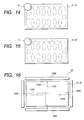
- the rotary head 9 is moved linearly while being revolved about an axis separate from its central axis. It should be noted that the illustration of the via holes 24 is omitted from Fig. 14.
- a fifth embodiment of this invention is similar to the first embodiment thereof except for design changes mentioned hereafter.
- the rotary head 9 is moved linearly while being rotated about its central axis and being revolved about an axis separate from its central axis.
- the rotary head 9 can force the electrically conductive paste 50 into each of the via holes 24 along every direction toward the via hole 24. It should be noted that the illustration of the via holes 24 is omitted from Fig. 15.
- Fig. 16 shows a portion of a charging apparatus 1A according to a sixth embodiment of this invention.
- the charging apparatus 1A in Fig. 16 is similar to the charging apparatus 1 in Fig. 1 except for design changes mentioned hereafter.
- the charging apparatus 1A includes squeegees 109A, 109B, 109C, and 109D instead of the rotary head 9 (see Fig. 1).
- Each of the squeegees 109A, 109B, 109C, and 109D functions as a means for forcing the electrically conductive paste 50 into the via holes 24 in the single-sided conductor-pattern film 21.
- the squeegees 109A and 109C oppose each other.
- the squeegees 109B and 109D oppose each other.
- the squeegees 109A, 109B, 109C, and 109D are moved linearly along the upper surface of the single-sided conductor-pattern film 21 (that is, the upper surface of the protective film 81 on the single-sided conductor-pattern film 21) in directions 110A, 110B, 110C, and 110D respectively.
- the directions 110A and 110C are opposite to each other.
- the directions 110B and 110D are opposite to each other.
- the directions 110A and 110C are perpendicular to the directions 110B and 110D.
- the squeegees 109A, 109B, 109C, and 109D force the electrically conductive paste 50 into each of the via holes 24 along four different directions corresponding to the directions 110A, 110B, 110C, and 110D. It should be noted that the illustration of the via holes 24 is omitted from Fig. 16.
- a seventh embodiment of this invention is similar to the first embodiment thereof except for design changes mentioned hereafter.
- each of the recesses 94 in the lower end surface of the pad member 91 has the shape of a slit rather than a hemisphere.
- the eighth embodiment of this invention is similar to the first embodiment thereof except for design changes mentioned hereafter.
- the eighth embodiment of this invention includes a feeding means provided separately of the rotary head 9 which functions as the forcing means.
- the feeding means supplies the electrically conductive paste 50 onto the upper surface of the single-sided conductor-pattern film 21.
- the feeding means is located at a position in front of the forcing means (the rotary head 9) as viewed in the direction of movement of the forcing means.
- a ninth embodiment of this invention is similar to the first embodiment thereof except for design changes mentioned hereafter.
- two or more single-sided conductor-pattern films 21 are juxtaposed on the upper surface of the table 3.
- the apparatus 1 charges via holes 24 in the single-sided conductor-pattern films 21 with the electrically conductive paste 50.
- a tenth embodiment of this invention is similar to the first embodiment thereof except for design changes mentioned hereafter.
- the walls defining the via holes 24 are coated with metal layers by plating, and the apparatus 1 charges inner spaces of the metal layers with fluid material such as liquefied resin.
- the metal layers in the via holes 24 function to provide electrical connection between the conductor patterns 22 on the single-sided conductor-pattern films 21.
- each of the resin films 23 and the cover layers 36a and 36b uses a film made by adding a non-conductive filler to polyether ether keton resin and polyether imide resin.
- each of the resin films 23 and the cover layers 36a and 36b may uses a film made of only polyether ether keton or polyether imide.
- each of the resin films 23 and the cover layers 36a and 36b uses a thermoplastic resin film made of polyethylene naphthalate, polyethylene terephthalate, polyether sulfone, thermoplastic polyimide, or liquid-crystal polymer.
- each of the resin films 23 and the cover layers 36a and 36b may use a thermosetting resin film made of B-stage epoxy resin, bismaleic triazine, polyphenylene ether, or polyimide.
- a thirteenth embodiment of this invention is similar to the first embodiment thereof except for design changes mentioned hereafter.
- a substrate made of resin or metal has holes, and the apparatus 1 charges the holes with fluid material such as liquefied resin.
- the holes Preferably, the holes have closed bottoms.
Landscapes
- Engineering & Computer Science (AREA)
- Manufacturing & Machinery (AREA)
- Microelectronics & Electronic Packaging (AREA)
- Mechanical Engineering (AREA)
- Printing Elements For Providing Electric Connections Between Printed Circuits (AREA)
- Production Of Multi-Layered Print Wiring Board (AREA)
- Manufacturing Of Printed Wiring (AREA)
- Screen Printers (AREA)
Abstract
Description
Claims (9)
- A method of charging a hole (24) in a substrate (23) with fluid material (50), comprising the steps of:supplying the fluid material (50) onto a surface of the substrate (23); andforcing the fluid material (50) into the hole (24) along at least three different directions on the surface of the substrate (23) to charge the hole (24) with the fluid material (50).
- A method as recited in claim 1, wherein the forcing step comprises:using a forcing means (9) placed on the surface of the substrate (23) in forcing the fluid material (50) into the hole (24); androtating the forcing means (9) about an axis perpendicular to the surface of the substrate (23) and moving the axis of rotation of the forcing member (9) along the surface of the substrate (23) to force the fluid material (50) into the hole (24) along the at least three different directions.
- A method as recited in claim 2, wherein the rotation of the forcing means (9) comprises one of rotation of the forcing member (9) about its central axis and revolution of the forcing member (9) about an axis separate from its central axis; and wherein the forcing step comprises simultaneously executing at least two of the rotation of the forcing member (9) about its central axis, the revolution of the forcing member (9) about the axis separate from its central axis, and linear motion of the forcing member (9).
- A method as recited in claim 1, wherein the forcing step comprises:using a forcing means (109A-109D) placed on the surface of the substrate (23) in forcing the fluid material (50) into the hole (24); andmoving the forcing means (109A-109D) in at least three different linear directions along the surface of the substrate (23) to force the fluid material (50) into the hole (24) along the at least three different directions.
- A method as recited in claim 1, wherein the hole (24) in the substrate (23) has a closed bottom.
- A method as recited in claim 1, wherein the substrate (23) comprises an insulating substrate (23), and the hole (24) comprises a via hole (24) in the insulating substrate (23).
- A method as recited in claim 6, wherein the insulating substrate (23) has a surface formed with a conductor pattern (22), and the via hole (24) has a bottom closed by the conductor pattern (22).
- A method as recited in claim 6, wherein the fluid material (50) comprises electrically conductive paste (50).
- A method as recited in claim 2, wherein the forcing means (9) comprises a forcing member (91) having a surface which faces the substrate (23) and which has recesses (94); and wherein the forcing step comprises holding the fluid material (50) in the recesses (94), and moving the fluid material (50) from the recesses (94) into the hole (24).
Applications Claiming Priority (2)
| Application Number | Priority Date | Filing Date | Title |
|---|---|---|---|
| JP2001232532 | 2001-07-31 | ||
| JP2001232532A JP3931600B2 (en) | 2001-07-31 | 2001-07-31 | Filling method of fluid substance |
Publications (2)
| Publication Number | Publication Date |
|---|---|
| EP1281519A1 true EP1281519A1 (en) | 2003-02-05 |
| EP1281519B1 EP1281519B1 (en) | 2007-03-07 |
Family
ID=19064444
Family Applications (1)
| Application Number | Title | Priority Date | Filing Date |
|---|---|---|---|
| EP02016674A Expired - Lifetime EP1281519B1 (en) | 2001-07-31 | 2002-07-25 | Method of charging hole with fluid material |
Country Status (9)
| Country | Link |
|---|---|
| US (1) | US20030026899A1 (en) |
| EP (1) | EP1281519B1 (en) |
| JP (1) | JP3931600B2 (en) |
| KR (1) | KR100501264B1 (en) |
| CN (1) | CN1231101C (en) |
| DE (1) | DE60218578T2 (en) |
| MX (1) | MXPA02007345A (en) |
| SG (2) | SG107109A1 (en) |
| TW (1) | TW540271B (en) |
Families Citing this family (6)
| Publication number | Priority date | Publication date | Assignee | Title |
|---|---|---|---|---|
| US8569632B2 (en) * | 2006-10-16 | 2013-10-29 | Napra Co., Ltd. | Wiring board having through hole or non-through hole, and method for producing the same |
| US20100031501A1 (en) * | 2008-08-08 | 2010-02-11 | Napra Co., Ltd. | Method for filling through hole or non-through hole formed on board with filler |
| JP5947098B2 (en) * | 2011-05-13 | 2016-07-06 | 株式会社半導体エネルギー研究所 | Method for manufacturing glass sealed body and method for manufacturing light-emitting device |
| KR20130085646A (en) * | 2012-01-20 | 2013-07-30 | 삼성전기주식회사 | Injection head for molten solder |
| KR101541153B1 (en) * | 2013-03-20 | 2015-08-03 | 주식회사 잉크테크 | System and method for making fine pattern |
| JP6328240B2 (en) * | 2014-07-04 | 2018-05-23 | 日立造船株式会社 | Electrostatic screen printer |
Citations (5)
| Publication number | Priority date | Publication date | Assignee | Title |
|---|---|---|---|---|
| JPH0393288A (en) | 1989-09-06 | 1991-04-18 | Matsushita Electric Ind Co Ltd | Screen printing apparatus for circuit pattern |
| US5254362A (en) | 1992-10-23 | 1993-10-19 | Motorola, Inc. | Method and apparatus for deposition of solder paste on a printed wiring board |
| JPH06234204A (en) | 1993-02-09 | 1994-08-23 | Matsushita Electric Ind Co Ltd | Screen printing device for cream solder |
| JPH1177957A (en) | 1997-09-17 | 1999-03-23 | Toshiba Corp | Solder paste printing method and apparatus |
| JPH11117937A (en) | 1997-08-15 | 1999-04-27 | Enomoto Co Ltd | Linear block |
Family Cites Families (8)
| Publication number | Priority date | Publication date | Assignee | Title |
|---|---|---|---|---|
| US3845712A (en) * | 1970-11-27 | 1974-11-05 | Armstrong Cork Co | Screen printing method |
| US4622239A (en) * | 1986-02-18 | 1986-11-11 | At&T Technologies, Inc. | Method and apparatus for dispensing viscous materials |
| US4919970A (en) * | 1986-09-15 | 1990-04-24 | International Business Machines Corporation | Solder deposition control |
| JP2761776B2 (en) * | 1989-10-25 | 1998-06-04 | Ii Ai Deyuhon De Nimoasu Ando Co | Method for manufacturing multilayer circuit board |
| JPH05131611A (en) * | 1991-11-12 | 1993-05-28 | Mitsubishi Electric Corp | Solder printer |
| US5478700A (en) * | 1993-12-21 | 1995-12-26 | International Business Machines Corporation | Method for applying bonding agents to pad and/or interconnection sites in the manufacture of electrical circuits using a bonding agent injection head |
| JPH07266541A (en) * | 1994-04-01 | 1995-10-17 | Takashi Nansai | Screen printing machine |
| US6461136B1 (en) * | 1999-08-26 | 2002-10-08 | International Business Machines Corp. | Apparatus for filling high aspect ratio via holes in electronic substrates |
-
2001
- 2001-07-31 JP JP2001232532A patent/JP3931600B2/en not_active Expired - Fee Related
-
2002
- 2002-07-24 US US10/201,156 patent/US20030026899A1/en not_active Abandoned
- 2002-07-25 EP EP02016674A patent/EP1281519B1/en not_active Expired - Lifetime
- 2002-07-25 SG SG200204551A patent/SG107109A1/en unknown
- 2002-07-25 DE DE60218578T patent/DE60218578T2/en not_active Expired - Lifetime
- 2002-07-25 SG SG200504902-8A patent/SG137693A1/en unknown
- 2002-07-29 MX MXPA02007345A patent/MXPA02007345A/en active IP Right Grant
- 2002-07-30 KR KR10-2002-0044886A patent/KR100501264B1/en not_active Expired - Fee Related
- 2002-07-30 TW TW091117051A patent/TW540271B/en active
- 2002-07-31 CN CNB021278628A patent/CN1231101C/en not_active Expired - Fee Related
Patent Citations (6)
| Publication number | Priority date | Publication date | Assignee | Title |
|---|---|---|---|---|
| JPH0393288A (en) | 1989-09-06 | 1991-04-18 | Matsushita Electric Ind Co Ltd | Screen printing apparatus for circuit pattern |
| US5254362A (en) | 1992-10-23 | 1993-10-19 | Motorola, Inc. | Method and apparatus for deposition of solder paste on a printed wiring board |
| JPH0768730A (en) | 1992-10-23 | 1995-03-14 | Motorola Inc | Device and method for making solder paste uniformly adhere on printed wiring board |
| JPH06234204A (en) | 1993-02-09 | 1994-08-23 | Matsushita Electric Ind Co Ltd | Screen printing device for cream solder |
| JPH11117937A (en) | 1997-08-15 | 1999-04-27 | Enomoto Co Ltd | Linear block |
| JPH1177957A (en) | 1997-09-17 | 1999-03-23 | Toshiba Corp | Solder paste printing method and apparatus |
Non-Patent Citations (1)
| Title |
|---|
| PATENT ABSTRACTS OF JAPAN vol. 018, no. 611 (M - 1708) 21 November 1994 (1994-11-21) * |
Also Published As
| Publication number | Publication date |
|---|---|
| DE60218578T2 (en) | 2007-11-22 |
| DE60218578D1 (en) | 2007-04-19 |
| SG107109A1 (en) | 2004-11-29 |
| CN1231101C (en) | 2005-12-07 |
| JP2003046234A (en) | 2003-02-14 |
| CN1400857A (en) | 2003-03-05 |
| KR100501264B1 (en) | 2005-07-18 |
| EP1281519B1 (en) | 2007-03-07 |
| KR20030011682A (en) | 2003-02-11 |
| TW540271B (en) | 2003-07-01 |
| MXPA02007345A (en) | 2004-08-11 |
| SG137693A1 (en) | 2007-12-28 |
| JP3931600B2 (en) | 2007-06-20 |
| US20030026899A1 (en) | 2003-02-06 |
Similar Documents
| Publication | Publication Date | Title |
|---|---|---|
| TWI423745B (en) | Wiring board with embedded components and manufacturing method thereof | |
| CN1107326C (en) | Inductor/capacitor combined element with variable capacitance and inductance | |
| WO2015006393A1 (en) | Fusion bonded liquid crystal polymer circuit structure | |
| US6695020B2 (en) | Fluid material filling apparatus and related filling methods | |
| CN101115353A (en) | Multilayer printed wiring board and manufacturing method thereof | |
| CN1554071A (en) | RFID connector with bridging circuit assembly and method of use | |
| EP3259965A1 (en) | Method for producing a printed circuit board | |
| US10159154B2 (en) | Fusion bonded liquid crystal polymer circuit structure | |
| US8327534B2 (en) | Method of fabricating printed circuit board assembly | |
| EP1281519B1 (en) | Method of charging hole with fluid material | |
| US20040134681A1 (en) | Circuit board and its manufacturing method | |
| JP2004111563A (en) | Multilayer circuit board having antenna and antenna structure using the same | |
| US20030061948A1 (en) | Reservoir stencil with relief areas | |
| KR100772454B1 (en) | Anisotropic conductive film and its manufacturing method | |
| TW200529718A (en) | Method for manufacturing circuit board, circuit board, and electronic equipment | |
| JP2000353872A (en) | Circuit board and method of manufacturing the same | |
| US12568584B2 (en) | Wiring board | |
| JP4536074B2 (en) | Method for transferring microball and method for manufacturing semiconductor device using the same | |
| JP3693421B2 (en) | Screen plate and screen printing device | |
| JPH0856064A (en) | Board with capacitor and manufacturing method thereof | |
| JP2001345528A (en) | Wiring board and its manufacturing method | |
| JPH06151508A (en) | Electrically connecting part and forming method thereof | |
| JP2019140161A (en) | Flexible wiring board manufacturing method and flexible wiring board | |
| JP2008034442A (en) | Method and apparatus for inserting conductive ball in printed circuit board | |
| JP2003211626A (en) | Screen printing method and screen printing apparatus |
Legal Events
| Date | Code | Title | Description |
|---|---|---|---|
| PUAI | Public reference made under article 153(3) epc to a published international application that has entered the european phase |
Free format text: ORIGINAL CODE: 0009012 |
|
| AK | Designated contracting states |
Designated state(s): AT BE BG CH CY CZ DE DK EE ES FI FR GB GR IE IT LI LU MC NL PT SE SK TR |
|
| AX | Request for extension of the european patent |
Extension state: AL LT LV MK RO SI |
|
| 17P | Request for examination filed |
Effective date: 20030515 |
|
| AKX | Designation fees paid |
Designated state(s): DE FR GB |
|
| 17Q | First examination report despatched |
Effective date: 20040629 |
|
| GRAP | Despatch of communication of intention to grant a patent |
Free format text: ORIGINAL CODE: EPIDOSNIGR1 |
|
| GRAS | Grant fee paid |
Free format text: ORIGINAL CODE: EPIDOSNIGR3 |
|
| GRAA | (expected) grant |
Free format text: ORIGINAL CODE: 0009210 |
|
| AK | Designated contracting states |
Kind code of ref document: B1 Designated state(s): DE FR GB |
|
| REG | Reference to a national code |
Ref country code: GB Ref legal event code: FG4D |
|
| REF | Corresponds to: |
Ref document number: 60218578 Country of ref document: DE Date of ref document: 20070419 Kind code of ref document: P |
|
| ET | Fr: translation filed | ||
| REG | Reference to a national code |
Ref country code: GB Ref legal event code: 746 Effective date: 20070912 |
|
| PLBE | No opposition filed within time limit |
Free format text: ORIGINAL CODE: 0009261 |
|
| STAA | Information on the status of an ep patent application or granted ep patent |
Free format text: STATUS: NO OPPOSITION FILED WITHIN TIME LIMIT |
|
| 26N | No opposition filed |
Effective date: 20071210 |
|
| PGFP | Annual fee paid to national office [announced via postgrant information from national office to epo] |
Ref country code: DE Payment date: 20100721 Year of fee payment: 9 Ref country code: FR Payment date: 20100805 Year of fee payment: 9 |
|
| PGFP | Annual fee paid to national office [announced via postgrant information from national office to epo] |
Ref country code: GB Payment date: 20100721 Year of fee payment: 9 |
|
| GBPC | Gb: european patent ceased through non-payment of renewal fee |
Effective date: 20110725 |
|
| REG | Reference to a national code |
Ref country code: FR Ref legal event code: ST Effective date: 20120330 |
|
| PG25 | Lapsed in a contracting state [announced via postgrant information from national office to epo] |
Ref country code: DE Free format text: LAPSE BECAUSE OF NON-PAYMENT OF DUE FEES Effective date: 20120201 Ref country code: FR Free format text: LAPSE BECAUSE OF NON-PAYMENT OF DUE FEES Effective date: 20110801 |
|
| REG | Reference to a national code |
Ref country code: DE Ref legal event code: R119 Ref document number: 60218578 Country of ref document: DE Effective date: 20120201 |
|
| PG25 | Lapsed in a contracting state [announced via postgrant information from national office to epo] |
Ref country code: GB Free format text: LAPSE BECAUSE OF NON-PAYMENT OF DUE FEES Effective date: 20110725 |