EP1280278A1 - Offset error compensation of input signals in analog-to-digital converter - Google Patents
Offset error compensation of input signals in analog-to-digital converter Download PDFInfo
- Publication number
- EP1280278A1 EP1280278A1 EP02102039A EP02102039A EP1280278A1 EP 1280278 A1 EP1280278 A1 EP 1280278A1 EP 02102039 A EP02102039 A EP 02102039A EP 02102039 A EP02102039 A EP 02102039A EP 1280278 A1 EP1280278 A1 EP 1280278A1
- Authority
- EP
- European Patent Office
- Prior art keywords
- analog
- signal
- input
- offset
- offset component
- Prior art date
- Legal status (The legal status is an assumption and is not a legal conclusion. Google has not performed a legal analysis and makes no representation as to the accuracy of the status listed.)
- Ceased
Links
Images



Classifications
-
- H—ELECTRICITY
- H03—ELECTRONIC CIRCUITRY
- H03M—CODING; DECODING; CODE CONVERSION IN GENERAL
- H03M1/00—Analogue/digital conversion; Digital/analogue conversion
- H03M1/10—Calibration or testing
- H03M1/1009—Calibration
- H03M1/1014—Calibration at one point of the transfer characteristic, i.e. by adjusting a single reference value, e.g. bias or gain error
- H03M1/1019—Calibration at one point of the transfer characteristic, i.e. by adjusting a single reference value, e.g. bias or gain error by storing a corrected or correction value in a digital look-up table
-
- H—ELECTRICITY
- H03—ELECTRONIC CIRCUITRY
- H03M—CODING; DECODING; CODE CONVERSION IN GENERAL
- H03M3/00—Conversion of analogue values to or from differential modulation
- H03M3/30—Delta-sigma modulation
- H03M3/38—Calibration
- H03M3/382—Calibration at one point of the transfer characteristic, i.e. by adjusting a single reference value, e.g. bias or gain error
- H03M3/384—Offset correction
-
- H—ELECTRICITY
- H03—ELECTRONIC CIRCUITRY
- H03M—CODING; DECODING; CODE CONVERSION IN GENERAL
- H03M1/00—Analogue/digital conversion; Digital/analogue conversion
- H03M1/10—Calibration or testing
- H03M1/1009—Calibration
- H03M1/1014—Calibration at one point of the transfer characteristic, i.e. by adjusting a single reference value, e.g. bias or gain error
- H03M1/1023—Offset correction
-
- H—ELECTRICITY
- H03—ELECTRONIC CIRCUITRY
- H03M—CODING; DECODING; CODE CONVERSION IN GENERAL
- H03M1/00—Analogue/digital conversion; Digital/analogue conversion
- H03M1/12—Analogue/digital converters
- H03M1/34—Analogue value compared with reference values
- H03M1/38—Analogue value compared with reference values sequentially only, e.g. successive approximation type
- H03M1/44—Sequential comparisons in series-connected stages with change in value of analogue signal
- H03M1/442—Sequential comparisons in series-connected stages with change in value of analogue signal using switched capacitors
-
- H—ELECTRICITY
- H03—ELECTRONIC CIRCUITRY
- H03M—CODING; DECODING; CODE CONVERSION IN GENERAL
- H03M1/00—Analogue/digital conversion; Digital/analogue conversion
- H03M1/12—Analogue/digital converters
- H03M1/34—Analogue value compared with reference values
- H03M1/38—Analogue value compared with reference values sequentially only, e.g. successive approximation type
- H03M1/46—Analogue value compared with reference values sequentially only, e.g. successive approximation type with digital/analogue converter for supplying reference values to converter
- H03M1/466—Analogue value compared with reference values sequentially only, e.g. successive approximation type with digital/analogue converter for supplying reference values to converter using switched capacitors
- H03M1/468—Analogue value compared with reference values sequentially only, e.g. successive approximation type with digital/analogue converter for supplying reference values to converter using switched capacitors in which the input S/H circuit is merged with the feedback DAC array
-
- H—ELECTRICITY
- H03—ELECTRONIC CIRCUITRY
- H03M—CODING; DECODING; CODE CONVERSION IN GENERAL
- H03M3/00—Conversion of analogue values to or from differential modulation
- H03M3/30—Delta-sigma modulation
- H03M3/458—Analogue/digital converters using delta-sigma modulation as an intermediate step
Definitions
- the invention relates to a method and circuit for compensating an offset component of an input signal (also referred to as a measurement signal) applied to an input of an analog-to-digital converter (ADC).
- ADC analog-to-digital converter
- the invention also relates to a method and circuit for compensating an offset component of an input signal applied to an input of a successive approximation register (SAR) ADC, or to compensating an offset component of an input signal applied to an input of any other type of switched capacitor ADC, such as a delta-sigma ADC, pipeline ADC, etc.
- SAR successive approximation register
- an analog input signal applied to the input of an ADC is a non-ideal signal.
- an analog input signal includes an offset component that occurs as a result of non-ideal behavior of a sensor, transducer, or other interface circuit generating the analog signal.
- an analog signal produced by a bridge circuit, Hall effect sensor or the like, or an analog encoder is likely to have a substantial offset voltage.
- the polarity of the offset voltage applied to the input of analog digital converter may not be certain.
- the offset component of the analog signal can be caused by temperature drift of the sensor or transducer.
- the offset component of the analog signal can be caused by a front-end buffer amplifier producing the analog signal in response to the signal produced by a sensor or other circuit.
- the construction of a sensor itself can be a source of the offset component of the analog input signal applied to the input of the ADC.
- an analog signal produced by a magnetic sensor may include an offset component caused by magnetization of the magnetic circuit.
- DSP digital signal processor
- microcontroller e.g., to measure the value of a positive peak (such as V + in Fig. 9) and the value of a negative peak (such as V - in Fig.
- the waveform of "prior art" Fig. 9 includes an "ideal" offset sinusoidal signal 6 having an amplitude of 1.5 volts, a peak-to-peak value 7 of 2 volts, and a positive offset of 0.5 volts.
- the 0.5 voltage offset causes the maximum value at point 9A of the waveform to be + 1.5 volts and the minimum value at point 9B to be -0.5 volts.
- a differential ADC which ordinarily would be needed to measure the 2 volt peak-to-peak value of the offset input signal 6 would require a 3 volt input range (-1.5 volts to plus 1.5 volts).
- the full-scale digital output signal produced by the ADC to represent the 2 volt peak-to-peak offset input signal 6 actually would be capable of representing a 3 volt peak-to-peak input signal having zero offset.
- the effective resolution of the analog-to-digital conversion of an offset analog input signal is inherently less than the effective resolution of an input signal of the same amplitude but having no offset.
- an object of the invention to provide an ADC capable of automatically compensating a high range of offset component errors in an analog input signal applied to the input of the ADC without requiring use of additional circuit components and without causing substantial delay in computing/determining an accurate digital output that accurately represents the true signal information contained in the analog input signal.
- the invention provides an analog-to-digital converter receiving an analog input signal (V IN ) including an offset component.
- the analog-to-digital converter includes a switched capacitor input circuit (101) configured to sample the analog input signal (V IN + ) to produce and store a signal representative of the sampled input signal on the first conductor (17).
- a conversion circuit (1) is coupled to the first conductor (17) and the switched capacitor input circuit (101), and is configured to produce a digital output signal (DATA OUT) representative of the analog input signal (V IN ).
- An offset correction circuit (4) includes an output coupled to the a second conductor (27), and also includes an input receiving a digital offset correction signal (DATA IN).
- the offset correction circuit (4) includes a switched capacitor correction circuit (4A) operative in response to the offset correction control signal (DATA IN) to transfer charge to or from the first conductor (17).
- the portion of the conversion circuit (1) connected to the first conductor (17) operates in response to adjustment by the offset correction circuit (4) of a signal conducted by the second conductor (27) so as to produce the digital output signal (DATA OUT) compensated for the offset component.
- successive approximation analog-to digital converter 100 includes an input stage 101 which receives a differential input signal V IN that is equal to the difference between a "positive” input signal V IN+ applied to input conductor 10 and a "negative” input signal V IN- applied to input conductor 20.
- Input stage 101 includes a "positive" section 101A that receives V IN+ and, in response thereto, produces the signal V CPOS on conductor 17, which is connected to the (+) input of a comparator 31.
- Input stage 101 also includes a "negative" section 101B that receives V IN- on conductor 20 and, in response thereto, produces the signal V CNEG on conductor 27, which is connected to the (-) input of comparator 31. Comparator 31 produces an output signal V COMP on conductor 3.
- Conductor 17 also is connected to an input of a conventional SAR (successive approximation register) circuit 1, which determines successive bits of the digital output DATA OUT by successively testing individual parallel, binarily weighted capacitors collectively represented by C P to determine if the charge stored thereon causes comparator 31 to produce a "1" or a "0" of the signal V COMP on the comparator output conductor 3 so as to test the corresponding bit of DATA OUT according to the conventional successive approximation analog-to-digital conversion technique.
- SAR conversion circuit 1 sequentially produces the N-bit digital output signal DATA OUT on bus 2 in response to the testing of the individual binarily weighted capacitors represented by C P .
- Positive section 101A of input stage 100 includes an input switch 11 connected between input conductor 10 and the left terminal of capacitor 14, which has a capacitance C and also is referred to as capacitor C P1 .
- the left terminal of capacitor C P1 also is connected to one terminal of a switch 12, which selectively connects the left terminal of capacitor C P1 to either V REF or V GND .
- the right terminal of capacitor C P1 is connected to conductor 17, which is also connected to one terminal of a switch 16 and to the (+) input of comparator 31 and to SAR network 1.
- Negative section 101B includes a switch 21 connected between input conductor 20 and the left terminal of a capacitor 24, which has a capacitance C and also is referred to as capacitor C N1 .
- the left terminal of capacitor C N1 also is connected to one terminal of a switch 22, which is selectively connected to either V REF or V GND .
- the right terminal of capacitor C N1 is connected to conductor 27, which is also connected to one terminal of a switch 26 and to the (-) input of comparator 31 and to offset correction network 4.
- the other terminal of each of switches 16 and 26 is connected to conductor 20, the voltage of which is V MID .
- Conductor 27 also is connected to an offset correction circuit 4 that, in accordance with the present invention, automatically corrects or compensates an offset component that may be included in the input signal V IN .
- Block 18 in Fig. 1 represents an external (although it could be internal) control circuit/system that is connected to bus 2 to receive DATA OUT.
- the control system 18, which can be readily implemented by means of a microprocessor or a digital signal processor (DSP), can operate in a first mode to cause analog-to-digital converter 100 to measure and store the maximum and minimum values (such as V + and V - in Fig.
- DSP digital signal processor
- control system 18 can operate in a second mode to cause analog-to-digital converter 100 to measure a steady-state value of an analog input signal V IN (i.e., the common mode voltage), which by definition is equal to the offset component of V IN .
- V IN analog input signal
- some transducers are capable of producing a steady-state signal equal to the offset component signal thereof, and that some other transducers are not capable of producing a steady-state signal upon which an AC component representing a quantity measured by the transducer is superimposed.
- the analog-to-digital conversion system shown in Fig. 1 is capable of compensating for the offset component of either kind of analog input signal.
- An offset correction circuit 4 includes a group of parallel-connected, binarily weighted capacitors represented by C N , each of which is selectively connected to either V REF or V GND according to the value of DATA IN, so as to automatically compensate (i.e., effectively cancel) the offset component of V IN , so that the digital output signal DATA OUT has a full-scale value equal to the magnitude of the analog input signal V IN plus or minus the magnitude of the offset component thereof (because the polarity of the offset component can be positive or negative).
- the binarily weighted capacitors C N21 , C N22 ...C N2J are referenced to ground.
- Fig. 2 shows input stage 101 of the SAR ADC 100 in slightly more detail than Fig. 1.
- a capacitor 25 which has a capacitance C and is also referred to as capacitor C N2
- capacitor C N2 is connected between conductor 27 and V GND .
- a capacitor 15 which has a capacitance C and is also referred to as capacitor C P2
- capacitor C P2 and switch 13 in Fig. 2 represent a group of binarily weighted capacitors and associated switches included in a portion 1A of SAR conversion circuit 1 in Fig. 1.
- switches 16 and 26 are closed to prepare for sampling of the measured input signal V IN .
- This causes the (-) and (+) inputs of comparator 31 both to be equal to the mid-point voltage V MID .
- the next step to prepare for of sampling the measured input voltage V IN involves closing the switches represented by reference switch 13 to connect one plate of each of the capacitors represented by C P2 to the ground voltage V GND. Then, the ADC is ready for the actual sampling of the measured input signal V IN , which is initiated by closing input switches 11 and 21, with switches 12 and 22 remaining open.
- Fig. 3 shows the circuit configuration for charging capacitors C P1 and C P2 during the input sampling process.
- Fig. 3 shows switch 11 closed, connecting V IN + to the left terminal of capacitor C P1.
- Switch 13 connects the left terminal of capacitor C P2 to V GND .
- Switch 16 is closed, connecting conductor 17 to V MID and conductor 27.
- Equation 1 shown below.
- Equation 2 A similar circuit configuration, not shown, can be drawn to represent the charging of capacitors C N1 and C N2, which is represented by Equation 2, also shown below:.
- Fig. 4 shows an equivalent circuit which illustrates the above mentioned process of switching capacitors C P1 and C P2 , which is defined by Equation 3, shown below.
- Fig. 4 shows switch 12 connecting the left terminal of capacitor C P1 to V REF , and also shows switch 13 connecting the left terminal of capacitor C P2 to V GND .
- a similar equivalent circuit (not shown) can be drawn to illustrate the process of charging capacitors C N1 and C N2 , which is defined by Equation 4, also shown below.
- Q PC 1 ( V CPOS - V REF ) ⁇ C P 1 + ( V CPOS - V GND ) ⁇ C P 2
- Q NC 1 ( V CNEG - V REF ) ⁇ C N 1 + ( V CNEG - V GND ) ⁇ C N 2
- Equations 5 and 6 determine the voltages V CPOS and V CNEG applied to the (+) and (-) inputs , respectively, of comparator 31 as a function of the input voltages V IN+ and V IN- .
- capacitors C N1 and C N2 are of the same capacitance C as capacitors C P1 and C P2 .
- C P2 represents a parallel connection of capacitors C P21 , C P22 ...C PN , where N is the resolution of the ADC. (For example, for a 10-bit ADC, N is equal to 10.)
- the capacitances of C P1 and C P2 have the same value C.
- the capacitors C P21 , C P22 ...C PN have the capacitance values of C/2°, C/2 1 ...C/2 N , and their sum will be equal to C. This is illustrated in Fig.
- capacitor C P2 represented by reference character 1A is represented by N capacitors C P21 , C P22 ...C PN , each having its right terminal connected to conductor 17 and its left terminal connected by a corresponding switch 151-1,2...N to either V REF or V GND (in response to the results of the previous comparison by comparator 31 and the conventional control circuitry in block 1 of Fig. 1).
- capacitor C N2 in Fig.2 is replaced in Fig. 6 by capacitors C N21 , C N22 ...C N2J , where J is the number of bits required to achieve the desired precision of the compensation. As shown in Fig.
- Offset correction circuitry 4A includes the J capacitors C N21 , C N22 ...C N2J each having its right terminal connected to conductor 27.
- preparation for sampling of the input signal V IN- begins by closing switch 26, which causes the voltage V CNEG applied to the (-) of comparator 31 to be equal to V MID
- switches 231-1,2...J are operated to connect the left plates of capacitors C N21 , C N22 ...C N2J to V REF or V GND according to the value of DATA IN (only after sampling, because at the beginning of the sampling of V IN , all of the switches 231-1,2...J are closed due to V GND ), and switch 22 remains open.
- the actual sampling of V IN- then begins by closing input switch 21.
- Fig. 7 shows an equivalent circuit which the represents the resulting charging of capacitor C N1 and capacitors C N21 , C N22 ...C N2J although for convenience, only the first two of capacitors C N21 , C N22 ...C N2J (namely C N21 and C N22 ) are shown.
- the equivalent circuit of Fig. 7 shows switch 21 closed to connect the left terminal of capacitor C N1 to V IN- , and also shows switch 26 closed to connect conductor 27 to V MID .
- Switch 231-1 connects the left terminal of capacitor C N21 to V GND .
- Switch 231-2 connects the left terminal of capacitor C N22 to V GND .
- the next step in the analog-to-digital conversion and offset cancellation process includes opening switch 26 so that the negative voltage V CNEG applied by conductor 27 to the (-) input of comparator 31 is no longer connected to V MID and the charge Q NS is frozen on capacitors C N21 , C N22 ...C N2J . Then input switch 21 is opened. To begin the comparison process by comparator 31, switch 22 is operated, for example, to connect the left plates of capacitor C N1 to V REF and switch 231-2 switches the left terminal of capacitor C N22 from V GND to V REF , in response to the present value of the DATA IN signal for this example. This results in the circuit structure illustrated in the equivalent circuit shown in Fig. 8. The equivalent circuit of Fig.
- Equation 11 the first three terms in Equation 11 constitute Equation 7.
- the remaining terms in Equation 11 represent the addition or subtraction of the offset component of the input signal V IN- .
- the voltage V CNEG is a function of the input voltage V IN- , and is offset by an amount which is a function of the constant reference voltage V REF and of the capacitance of the selectable combination of capacitors C N1 and C N21 , C N22 ...C N2J , that selectable combination being determined by the value of the offset compensation control signal DATA IN.
- a single-ended input voltage referenced to ground can be applied to either of input terminals 10 or 20, with the other input terminal being connected to an internal fixed reference voltage, or preferably, an external fixed reference voltage, such as V REF or V GND .
- V REF external fixed reference voltage
- V GND external fixed reference voltage
- Fig. 10A shows a block diagram wherein the offset error compensation technique of the present invention is utilized to compensate a delta sigma ADC or a pipeline ADC designated by reference numeral 40.
- the digital output signal DATA OUT is provided as an input to a control system 18, which generates an offset compensation signal DATA IN.
- the offset compensation signal DATA IN then controls the various switches of a pair of binarily weighted capacitors in each of a pair of offset compensation networks 4A and 4B.
- the input signal V IN+ applied to input conductor 10 is coupled by an input capacitor C IN+ to a charge summing conductor 17 connected to the (+) of ADC 40.
- Conductor 17 also is connected to one terminal of each of the binarily weighted (or otherwise weighted) compensation capacitors of switched capacitor compensation circuit 4A and to one terminal of a feedback capacitor 41A, the other terminal of which is connected to the serial DATA OUT conductor 2.
- the input signal V IN + applied to input conductor 20 is coupled by an input capacitor C IN - to a charge summing conductor 27 connected to the (-) of ADC 40.
- Conductor 27 also is connected to one terminal of each of the binarily weighted (or otherwise weighted) compensation capacitors of a second switched capacitor compensation circuit 4B and to one terminal of a feedback capacitor 41B, the other terminal of which is connected to the serial DATA OUT conductor 2.
- Fig. 10B shows a variation of the embodiment of Fig. 10A in which the second switched capacitor compensation circuit 4B is omitted.
- An important advantage of the invention is that the full-scale output of the ADC can represent a larger amplitude of an AC component of an analog input signal, so, in effect, the ADC resolution is increased compared to the situation wherein the offset component of the analog input signal is not automatically compensated.
- Another advantage of the invention is that it provides an ADC that is especially useful to compensate any sensor offset, especially in controlling motors. Also, the invention reduces the software overhead required by some prior art techniques for compensating an offset component of an input signal.
- the offset correction circuit 4 of Fig. 1 could be connected to a node similar to node 27 in a switched capacitor analog input signal sampling stage of another analog-to-digital converters than a SAR ADC, such as a delta sigma ADC or a pipeline ADC.
Landscapes
- Engineering & Computer Science (AREA)
- Theoretical Computer Science (AREA)
- Analogue/Digital Conversion (AREA)
Abstract
Description
- The invention relates to a method and circuit for compensating an offset component of an input signal (also referred to as a measurement signal) applied to an input of an analog-to-digital converter (ADC). The invention also relates to a method and circuit for compensating an offset component of an input signal applied to an input of a successive approximation register (SAR) ADC, or to compensating an offset component of an input signal applied to an input of any other type of switched capacitor ADC, such as a delta-sigma ADC, pipeline ADC, etc.
- In most cases, an analog input signal applied to the input of an ADC is a non-ideal signal. Typically, such an analog input signal includes an offset component that occurs as a result of non-ideal behavior of a sensor, transducer, or other interface circuit generating the analog signal. For example, an analog signal produced by a bridge circuit, Hall effect sensor or the like, or an analog encoder, is likely to have a substantial offset voltage. The polarity of the offset voltage applied to the input of analog digital converter may not be certain.
- The offset component of the analog signal can be caused by temperature drift of the sensor or transducer. Or, the offset component of the analog signal can be caused by a front-end buffer amplifier producing the analog signal in response to the signal produced by a sensor or other circuit. The construction of a sensor itself can be a source of the offset component of the analog input signal applied to the input of the ADC. For example, an analog signal produced by a magnetic sensor may include an offset component caused by magnetization of the magnetic circuit. Even though modern design of various sensors and associated front-end electronics (such as buffer amplifiers) tends to minimize the magnitude of the offset component of the measurement signal, the offset component nevertheless often is sufficiently large to be problematic, for example, by masking or obstructing useful signal information contained in the measurement signal.
- Consequently, numerous software techniques and hardware techniques have been developed to extract useful signal information from the measurement signal. Typical hardware techniques include compensating the offset component error to provide a "clean" analog signal to the input of the ADC, but this solution to the problem may not be cost-effective because of the cost of additional circuit components. Software solutions of the problems caused by offset components generally require more computing time by a digital signal processor (DSP) or microcontroller or the like (e.g., to measure the value of a positive peak (such as V+ in Fig. 9) and the value of a negative peak (such as V- in Fig. 9) of the measurement signal and divide the sum thereof by 2 to obtain the offset value (V+ + V-)/2, or to measure a "steady-state" value of the measurement signal which is equal to the offset value). The delay may be unacceptable in time-critical applications.
- The waveform of "prior art" Fig. 9 includes an "ideal" offset
sinusoidal signal 6 having an amplitude of 1.5 volts, a peak-to-peak value 7 of 2 volts, and a positive offset of 0.5 volts. The 0.5 voltage offset causes the maximum value atpoint 9A of the waveform to be + 1.5 volts and the minimum value atpoint 9B to be -0.5 volts. - Referring to Fig. 9, it should be understood that, to convert the offset
sinusoidal signal 6 to a digital representation, a differential ADC which ordinarily would be needed to measure the 2 volt peak-to-peak value of theoffset input signal 6 would require a 3 volt input range (-1.5 volts to plus 1.5 volts). The full-scale digital output signal produced by the ADC to represent the 2 volt peak-to-peakoffset input signal 6 actually would be capable of representing a 3 volt peak-to-peak input signal having zero offset. Thus, the effective resolution of the analog-to-digital conversion of an offset analog input signal is inherently less than the effective resolution of an input signal of the same amplitude but having no offset. - Accordingly, it is an object of the invention to provide an ADC capable of automatically compensating a high range of offset component errors in an analog input signal applied to the input of the ADC without requiring use of additional circuit components and without causing substantial delay in computing/determining an accurate digital output that accurately represents the true signal information contained in the analog input signal.
- It is another object of the invention to avoid the loss of resolution that ordinarily occurs as a result of analog-to-digital conversion of an input signal having a substantial offset component.
- Is another object of the invention to reduce or eliminate the software overhead required for extracting useful information from a measurement signal.
- Briefly described, and in accordance with one embodiment thereof, the invention provides an analog-to-digital converter receiving an analog input signal (VIN) including an offset component. The analog-to-digital converter includes a switched capacitor input circuit (101) configured to sample the analog input signal (VIN +) to produce and store a signal representative of the sampled input signal on the first conductor (17). A conversion circuit (1) is coupled to the first conductor (17) and the switched capacitor input circuit (101), and is configured to produce a digital output signal (DATA OUT) representative of the analog input signal (VIN). An offset correction circuit (4) includes an output coupled to the a second conductor (27), and also includes an input receiving a digital offset correction signal (DATA IN). The offset correction circuit (4) includes a switched capacitor correction circuit (4A) operative in response to the offset correction control signal (DATA IN) to transfer charge to or from the first conductor (17). The portion of the conversion circuit (1) connected to the first conductor (17) operates in response to adjustment by the offset correction circuit (4) of a signal conducted by the second conductor (27) so as to produce the digital output signal (DATA OUT) compensated for the offset component.
-
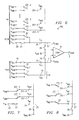
- Fig. 1 is a partial schematic diagram illustrating the automatic input signal offset correction system of the present invention.
- Fig. 2 what is a schematic diagram of an input stage of a SAR ADC without offset compensation.
- Fig. 3 is a schematic diagram of equivalent circuitry useful in explaining charging of capacitors CP1 and CP2 during the input sampling portion of the operation of the ADC of Fig. 1.
- Fig. 4 is a schematic diagram of circuitry useful in explaining charging of capacitors CP1 and CP2 during the conversion portion of the operation of the ADC of Fig. 1.
- Fig. 5 is a schematic diagram similar to Fig. 2, and is useful in explaining the conversion process of the operation of a SAR ADC.
- Fig. 6 is a schematic diagram illustrating the circuitry included in the input stage of the ADC of Fig. 1 for compensating offset in the input signal.
- Fig. 7 is a schematic diagram of an equivalent circuit useful in explaining the charging of certain capacitors in the input stage of the ADC of Figs.1 and 6 during the input sampling and offset compensation portion of the operation of the ADC.
- Fig. 8 is a schematic diagram of another equivalent circuit useful in explaining the charging of certain capacitors in the input stage of the ADC of Figs. 1 and 6 during the conversion and offset compensation portion of the operation of the ADC.
- Fig. 9 is a waveform of a typical analog input signal having an offset component.
- Fig. 10A is a block diagram illustrating an embodiment of the invention including an ADC other than a SAR type of ADC.
- Fig. 10B is a block diagram of a variation of the embodiment of Fig. 2A.
- Referring to Fig. 1, successive approximation analog-to
digital converter 100, hereinafter referred to simply asADC 100, includes aninput stage 101 which receives a differential input signal VIN that is equal to the difference between a "positive" input signal VIN+ applied toinput conductor 10 and a "negative" input signal VIN- applied toinput conductor 20.Input stage 101 includes a "positive"section 101A that receives VIN+ and, in response thereto, produces the signal VCPOS onconductor 17, which is connected to the (+) input of acomparator 31.Input stage 101 also includes a "negative" section 101B that receives VIN- onconductor 20 and, in response thereto, produces the signal VCNEG onconductor 27, which is connected to the (-) input ofcomparator 31.Comparator 31 produces an output signal VCOMP onconductor 3. -
Conductor 17 also is connected to an input of a conventional SAR (successive approximation register)circuit 1, which determines successive bits of the digital output DATA OUT by successively testing individual parallel, binarily weighted capacitors collectively represented by CP to determine if the charge stored thereoncauses comparator 31 to produce a "1" or a "0" of the signal VCOMP on thecomparator output conductor 3 so as to test the corresponding bit of DATA OUT according to the conventional successive approximation analog-to-digital conversion technique.SAR conversion circuit 1 sequentially produces the N-bit digital output signal DATA OUT onbus 2 in response to the testing of the individual binarily weighted capacitors represented by CP.
Positive section 101A ofinput stage 100 includes aninput switch 11 connected betweeninput conductor 10 and the left terminal ofcapacitor 14, which has a capacitance C and also is referred to as capacitor CP1. The left terminal of capacitor CP1 also is connected to one terminal of aswitch 12, which selectively connects the left terminal of capacitor CP1 to either VREF or VGND . The right terminal of capacitor CP1 is connected toconductor 17, which is also connected to one terminal of aswitch 16 and to the (+) input ofcomparator 31 and toSAR network 1. - Negative section 101B includes a
switch 21 connected betweeninput conductor 20 and the left terminal of acapacitor 24, which has a capacitance C and also is referred to as capacitor CN1. The left terminal of capacitor CN1 also is connected to one terminal of aswitch 22, which is selectively connected to either VREF or VGND. The right terminal of capacitor CN1 is connected toconductor 27, which is also connected to one terminal of aswitch 26 and to the (-) input ofcomparator 31 and to offset correction network 4. The other terminal of each ofswitches conductor 20, the voltage of which is VMID. -
Conductor 27 also is connected to an offset correction circuit 4 that, in accordance with the present invention, automatically corrects or compensates an offset component that may be included in the input signal VIN. Block 18 in Fig. 1 represents an external (although it could be internal) control circuit/system that is connected tobus 2 to receive DATA OUT. Thecontrol system 18, which can be readily implemented by means of a microprocessor or a digital signal processor (DSP), can operate in a first mode to cause analog-to-digital converter 100 to measure and store the maximum and minimum values (such as V+ and V- in Fig. 9) of the input signal VIN and computes the peak-to-peak value of VIN and the magnitude and polarity of the offset component of VIN, and then accordingly produces a value of the digital compensation signal DATA IN, which is needed to compute the offset component of VIN. - Also,
control system 18 can operate in a second mode to cause analog-to-digital converter 100 to measure a steady-state value of an analog input signal VIN (i.e., the common mode voltage), which by definition is equal to the offset component of VIN. It should be appreciated that some transducers are capable of producing a steady-state signal equal to the offset component signal thereof, and that some other transducers are not capable of producing a steady-state signal upon which an AC component representing a quantity measured by the transducer is superimposed. The analog-to-digital conversion system shown in Fig. 1 is capable of compensating for the offset component of either kind of analog input signal. - An offset correction circuit 4 includes a group of parallel-connected, binarily weighted capacitors represented by CN, each of which is selectively connected to either VREF or VGND according to the value of DATA IN, so as to automatically compensate (i.e., effectively cancel) the offset component of VIN, so that the digital output signal DATA OUT has a full-scale value equal to the magnitude of the analog input signal VIN plus or minus the magnitude of the offset component thereof (because the polarity of the offset component can be positive or negative). During sampling of VIN, the binarily weighted capacitors CN21, CN22...CN2J are referenced to ground.
- Fig. 2 shows
input stage 101 of theSAR ADC 100 in slightly more detail than Fig. 1. In Fig. 2, acapacitor 25, which has a capacitance C and is also referred to as capacitor CN2, is connected betweenconductor 27 and VGND. Similarly, acapacitor 15, which has a capacitance C and is also referred to as capacitor CP2, is connected betweenconductor 17 and one terminal of single pole,double throw switch 13, the single pole of which is selectively connected to either VREF or VGND. As subsequently explained, capacitor CP2 and switch 13 in Fig. 2 represent a group of binarily weighted capacitors and associated switches included in aportion 1A ofSAR conversion circuit 1 in Fig. 1. - Still referring to Fig. 2, switches 16 and 26 are closed to prepare for sampling of the measured input signal VIN. This causes the (-) and (+) inputs of
comparator 31 both to be equal to the mid-point voltage VMID. The next step to prepare for of sampling the measured input voltage VIN involves closing the switches represented byreference switch 13 to connect one plate of each of the capacitors represented by CP2 to the ground voltage VGND. Then, the ADC is ready for the actual sampling of the measured input signal VIN, which is initiated by closing input switches 11 and 21, withswitches - After an initial transition period of the input sampling process, the voltages on
conductors conductor 17 to VMID andconductor 27. This results in the charging of capacitors CP1 and CP2, which is represented byEquation 1, shown below. A similar circuit configuration, not shown, can be drawn to represent the charging of capacitors CN1 and CN2, which is represented byEquation 2, also shown below:.

- After the charging processes of
Equations switches conductor 17, applied to the (+) input ofcomparator 31, and VCNEG is the voltage onconductor 27, applied to the (-) input ofcomparator 31. - Fig. 4 shows an equivalent circuit which illustrates the above mentioned process of switching capacitors CP1 and CP2, which is defined by
Equation 3, shown below. Fig. 4 shows switch 12 connecting the left terminal of capacitor CP1 to VREF, and also showsswitch 13 connecting the left terminal of capacitor CP2 to VGND. A similar equivalent circuit (not shown) can be drawn to illustrate the process of charging capacitors CN1 and CN2, which is defined by Equation 4, also shown below.

- The charging of capacitor CP1 and capacitor CP2 during the sampling operation is the same as during the conversion operation, because charge from
conductor 17 cannot go anywhere else. CombiningEquation 1 andEquation 3, and setting VGND equal to 0 results inEquation 5, shown below:
- A similar procedure applies to the negative side 101B of the
input stage 101, wherein the charging of capacitors CN1 and CN2 is the same during the sampling operation and the conversion operation, so combiningEquation 2 and Equation 4 and setting VGND equal to 0 results inEquation 6, shown below:
- Thus,
Equations comparator 31 as a function of the input voltages VIN+ and VIN-. Typically, capacitors CN1 and CN2 are of the same capacitance C as capacitors CP1 and CP2. The voltage VCNEG determined according toEquation 6 is constant during the entire conversion, and can be described by Equation 7, shown below:
- At this point, it should be understood that in Figs. 2, 3 and 4, CP2 represents a parallel connection of capacitors CP21, CP22...CPN, where N is the resolution of the ADC. (For example, for a 10-bit ADC, N is equal to 10.) Ordinarily, the capacitances of CP1 and CP2 have the same value C. In that case, the capacitors CP21, CP22...CPN have the capacitance values of C/2°, C/21...C/2N, and their sum will be equal to C. This is illustrated in Fig. 5, wherein the capacitor CP2 represented by
reference character 1A is represented by N capacitors CP21, CP22...CPN, each having its right terminal connected toconductor 17 and its left terminal connected by a corresponding switch 151-1,2...N to either VREF or VGND (in response to the results of the previous comparison bycomparator 31 and the conventional control circuitry inblock 1 of Fig. 1). - It should be noted that the described embodiment of the invention automatically offsets the negative voltage VCNEG during, rather than before or after, the analog-to-digital conversion, so that offset error components of the input signals VIN+ and VIN- are, in effect, automatically removed during the conversion . To accomplish automatic compensation or cancellation of the offset error of the input signal during the conversion, capacitor CN2 in Fig.2 is replaced in Fig. 6 by capacitors CN21, CN22...CN2J, where J is the number of bits required to achieve the desired precision of the compensation. As shown in Fig. 6, additional switches 231-1, 231-2...231-J are connected to the left terminals of capacitors CN21, CN22...CN2J, respectively, to allow them each to be selectively connected to VREF or VGND in response to the digital offset compensation control signal DATA IN. In Fig. 6, a portion of the circuitry included in offset correction circuit 4 of Fig. 1 is included and is designated by
reference numeral 4A. Offsetcorrection circuitry 4A includes the J capacitors CN21, CN22...CN2J each having its right terminal connected toconductor 27. - Still referring to Fig. 6, preparation for sampling of the input signal VIN- begins by closing
switch 26, which causes the voltage VCNEG applied to the (-) ofcomparator 31 to be equal to VMID Then switches 231-1,2...J are operated to connect the left plates of capacitors CN21, CN22...CN2J to VREF or VGND according to the value of DATA IN (only after sampling, because at the beginning of the sampling of VIN, all of the switches 231-1,2...J are closed due to VGND), and switch 22 remains open. The actual sampling of VIN- then begins by closinginput switch 21. The above described connecting of the left plates of the capacitors CN21, CN22...CN2J to VGND during sampling and to VREF or VGND according to DATA IN during conversion produces an offset of one polarity or direction. To obtain an offset of the other polarity or direction, it is necessary to connect the left plates of the capacitors CN21, CN22...CN2J to VREF or VGND during sampling according to DATA IN and to VGND during the conversion. - Fig. 7 shows an equivalent circuit which the represents the resulting charging of capacitor CN1 and capacitors CN21, CN22...CN2J although for convenience, only the first two of capacitors CN21, CN22...CN2J (namely CN21 and CN22) are shown. The equivalent circuit of Fig. 7 shows switch 21 closed to connect the left terminal of capacitor CN1 to VIN-, and also shows
switch 26 closed to connectconductor 27 to VMID. Switch 231-1 connects the left terminal of capacitor CN21 to VGND. Switch 231-2 connects the left terminal of capacitor CN22 to VGND. The charging of capacitor CN2 and the first two of the capacitors CN21, CN22...CN2J (namely, capacitors CN21 and CN22) is represented byEquation 8, shown below:
- The next step in the analog-to-digital conversion and offset cancellation process includes opening
switch 26 so that the negative voltage VCNEG applied byconductor 27 to the (-) input ofcomparator 31 is no longer connected to VMID and the charge QNS is frozen on capacitors CN21, CN22...CN2J. Then inputswitch 21 is opened. To begin the comparison process bycomparator 31,switch 22 is operated, for example, to connect the left plates of capacitor CN1 to VREF and switch 231-2 switches the left terminal of capacitor CN22 from VGND to VREF, in response to the present value of the DATA IN signal for this example. This results in the circuit structure illustrated in the equivalent circuit shown in Fig. 8. The equivalent circuit of Fig. 8 shows switch 22 closed to connect the left terminal of capacitor CN1 to VREF. Switch 231-1 is closed to connect the left terminal of capacitor CN21 to VGND, and switch 231-2 is closed to connect the left terminal of capacitor CN22 to VREF. In the equivalent circuit of Fig. 8, which, for convenience shows only the first two of capacitors CN21, CN22...CN2J, the charging of capacitor CN1 and the first two of capacitors CN21, CN22...CN2J (namely capacitors CN21 and CN22) is described by Equation 9, shown below:
- The charging of capacitors CN1, CN21, CN22...CN2J is the same during both the sampling operation and conversion operation, so combining
Equation 8 and Equation 9 and setting VGND equal to 0 results inEquation 10, shown below:
- The capacitance of capacitor CN1 is equal to the sum of the capacitances of capacitors CN21, CN22...CN2J, which is equal to C, so substituting this expression in Equation10 results in
Equation 11, shown below:
- It can be seen that the first three terms in
Equation 11 constitute Equation 7. The remaining terms inEquation 11 represent the addition or subtraction of the offset component of the input signal VIN-. Thus, the voltage VCNEG is a function of the input voltage VIN-, and is offset by an amount which is a function of the constant reference voltage VREF and of the capacitance of the selectable combination of capacitors CN1 and CN21, CN22...CN2J, that selectable combination being determined by the value of the offset compensation control signal DATA IN. - The above described operation of analog-to-
digital converter 100 is for a differential input voltage VIN = VIN+ - VIN-. However, a single-ended input voltage referenced to ground can be applied to either ofinput terminals - Fig. 10A shows a block diagram wherein the offset error compensation technique of the present invention is utilized to compensate a delta sigma ADC or a pipeline ADC designated by
reference numeral 40. As in Fig. 1, the digital output signal DATA OUT is provided as an input to acontrol system 18, which generates an offset compensation signal DATA IN. The offset compensation signal DATA IN then controls the various switches of a pair of binarily weighted capacitors in each of a pair of offsetcompensation networks conductor 10 is coupled by an input capacitor CIN+ to acharge summing conductor 17 connected to the (+) ofADC 40.Conductor 17 also is connected to one terminal of each of the binarily weighted (or otherwise weighted) compensation capacitors of switchedcapacitor compensation circuit 4A and to one terminal of afeedback capacitor 41A, the other terminal of which is connected to the serial DATA OUTconductor 2. Similarly, the input signal VIN + applied to inputconductor 20 is coupled by an input capacitor CIN - to acharge summing conductor 27 connected to the (-) ofADC 40.Conductor 27 also is connected to one terminal of each of the binarily weighted (or otherwise weighted) compensation capacitors of a second switchedcapacitor compensation circuit 4B and to one terminal of a feedback capacitor 41B, the other terminal of which is connected to the serial DATA OUTconductor 2. Fig. 10B shows a variation of the embodiment of Fig. 10A in which the second switchedcapacitor compensation circuit 4B is omitted. - An important advantage of the invention is that the full-scale output of the ADC can represent a larger amplitude of an AC component of an analog input signal, so, in effect, the ADC resolution is increased compared to the situation wherein the offset component of the analog input signal is not automatically compensated. Another advantage of the invention is that it provides an ADC that is especially useful to compensate any sensor offset, especially in controlling motors. Also, the invention reduces the software overhead required by some prior art techniques for compensating an offset component of an input signal.
- While the invention has been described with reference to several particular embodiments thereof, those skilled in the art will be able to make the various modifications to the described embodiments of the invention without departing from the true spirit and scope of the invention. It is intended that all elements or steps which are insubstantially different or perform substantially the same function in substantially the same way to achieve the same result as what is claimed are within the scope of the invention. For example, the offset correction circuit 4 of Fig. 1 could be connected to a node similar to
node 27 in a switched capacitor analog input signal sampling stage of another analog-to-digital converters than a SAR ADC, such as a delta sigma ADC or a pipeline ADC.
Claims (25)
- An analog-to-digital converter receiving an analog input signal including an offset component, the analog-to-digital converter comprising:(a) a switched capacitor input circuit configured to sample the analog input signal to produce and store a signal representative of the sampled input signal between a first conductor and a second conductor;(b) a conversion circuit coupled to the first conductor and the switched capacitor input circuit and configured to produce a digital output signal representative of the analog input signal;(c) an offset correction circuit having an output coupled to the second conductor and an input receiving a digital offset correction signal, the offset correction circuit including a switched capacitor correction circuit operative in response to the offset correction control signal to transfer charge to/from the second conductor;(d) the conversion circuit being operative in response to adjustment by the offset correction circuit of a signal conducted by the first conductor to produce the digital output signal compensated for the offset component.
- The analog-to-digital converter of claim 1, wherein the analog-to-digital converter includes SAR (successive approximation register) analog-to-digital conversion circuitry.
- The analog-to-digital converter of claim 1, wherein the analog-to-digital converter includes delta-sigma analog-to-digital conversion circuitry.
- The analog-to-digital converter of claim 1, wherein the analog-to-digital converter includes pipeline analog-to-digital conversion circuitry.
- The analog-to-digital converter of claim 2, claim 3 or claim 4 wherein the analog input signal is a differential signal, and wherein the switched capacitor input circuit includes a first section including a first input terminal and a second section including a second input terminal, the differential input signal being applied between the first input terminal and the second input terminal.
- The analog-to-digital converter of claim 2, claim 3 or claim 4 wherein the analog input signal is a single-ended signal, and wherein the switched capacitor input circuit includes a first section including a first input terminal and a second section including a second input terminal, the second input terminal being connected to a constant reference voltage, the single-ended signal being applied to the first input terminal and the constant reference voltage being applied to the second input terminal.
- The analog-to-digital converter of claim 2, claim 3 or claim 4 wherein the analog input signal is a single-ended signal, and wherein the switched capacitor input circuit includes a first section including a first input terminal and a second section including a second input terminal, the first input terminal being connected to a constant reference voltage, the single-ended signal being applied to the second input terminal and the constant reference voltage being applied to the first input terminal.
- The analog-to-digital converter of claim 5, claim 6 or claim 7 wherein the first section includes a first switch coupled between the first input terminal and a first terminal of a first input capacitor and a second switch configured to selectively couple the first terminal of the first input capacitor to either a first reference voltage or a second reference voltage, a second terminal of the first input capacitor being coupled by a second conductor to a first input of a comparator.
- The analog-to-digital converter of claim 8 wherein the second section includes a third switch coupled between the second input terminal and a first terminal of a second input capacitor and a fourth switch coupled between the first reference voltage and the first conductor, the first conductor being coupled to a second input of the comparator.
- The analog-to-digital converter of claim 9 wherein the first section of the switched capacitor input stage includes a first group of binarily weighted capacitors each having a first terminal coupled to a corresponding switch, respectively, for selectively coupling the first terminal of that capacitor to either the first reference voltage or the second reference voltage, and a second terminal coupled to the second conductor.
- The analog-to-digital converter of claim 9 or claim 10 wherein the offset correction circuit includes a second group of binarily weighted capacitors each having a first terminal coupled to a corresponding switch, respectively, for selectively coupling the first terminal of that capacitor to either the first reference voltage or the second reference voltage, and a second terminal coupled to the first conductor.
- The analog-to-digital converter of claim 1 wherein the digital output signal is received by a control circuit which operates to measure and store peak values of the input signal and compute a magnitude and polarity of the offset component of the input signal, and produce a corresponding value of the offset correction control signal.
- The analog-to-digital converter of claim 12 wherein the control circuit is an external control circuit which includes a data processing circuit.
- The analog-to-digital converter of claim 13 wherein the data processing circuit includes a digital signal processor (DSP).
- The analog-to-digital converter of claim 13 or claim 14 wherein the data processing circuit includes a microprocessor.
- A method of avoiding loss of resolution in conversion of an analog input signal having an offset component to a digital signal, the method comprising:(a) determining a magnitude of the offset component;(b) producing an offset compensation control signal representative of the magnitude of the offset component; and(c) controlling a transfer of offset compensation charge into or out of a conductor in a switched capacitor input circuit of an analog-to-digital converter to adjust a signal representative of the analog input voltage being conducted by the first conductor so as to cause a conversion circuit of the analog-to-digital converter to produce a digital output signal having a full-scale value equal to the magnitude of the analog input signal plus or minus the magnitude of the offset component.
- The method of claim 16 wherein step (a) includes determining the polarity of the offset component.
- The method of claim 17 wherein step (a) includes measuring minimum and maximum peak values of the analog input signal by means of the analog-to-digital converter and using the peak values to compute a magnitude of the offset component and a polarity of the offset component and using the computed magnitude and polarity to produce the offset compensation signal.
- The method of claim 17 wherein step (a) includes measuring a steady state value of the analog input signal to produce a value of the digital signal representative of the magnitude and polarity of the offset component.
- The method of claim 17 wherein step (a) includes measuring a steady state value of the analog input signal to produce a value of the digital signal representative of the magnitude and polarity of the offset component if a transducer producing the analog input signal is controlled to produce a steady-state value which represents the offset component, and wherein step (a) includes measuring minimum and maximum peak values of the analog input signal by means of the analog-to-digital converter and using the peak values to compute a magnitude of the offset component and a polarity of the offset component and using the computed magnitude and polarity to produce the offset compensation signal if a transducer producing the analog input signal is not controlled to produce a steady-state value which represents the offset component.
- An analog-to-digital conversion system for avoiding loss of resolution in conversion of an analog input signal having an offset component to a digital signal, comprising:(a) means for determining a magnitude of the offset component;(b) means for producing an offset compensation control signal representative of the magnitude of the offset component; and(c) means for controlling a transfer of offset compensation charge into or out of a conductor in a switched capacitor input circuit of an analog-to-digital converter to adjust a signal representative of the analog input voltage being conducted by the first conductor so as to cause a conversion circuit of the analog-to-digital converter to produce a digital output signal having a full-scale value equal to the magnitude of the analog input signal plus or minus the magnitude of the offset component.
- The analog-to-digital conversion system of claim 21 wherein the means for determining a magnitude of the offset component also determines the polarity of the offset component.
- The analog-to-digital conversion system of claim 21 wherein the means for producing an offset compensation control signal includes means for measuring minimum and maximum peak values of the analog input signal by means of the analog-to-digital converter and using the peak values to compute a magnitude of the offset component and a polarity of the offset component and using the computed magnitude and polarity to produce the offset compensation signal.
- The analog-to-digital conversion system of claim 22 wherein the means for determining a magnitude and polarity of the offset component includes means for measuring a steady state value of the analog input signal to produce a value of the digital signal representative of the magnitude and polarity of the offset component.
- The analog-to-digital conversion system of claim 22 wherein the means for determining a magnitude and polarity of the offset component includes means for measuring a steady state value of the analog input signal to produce a value of the digital signal representative of the magnitude and polarity of the offset component if a transducer producing the analog input signal is controlled to produce a steady-state value which represents the offset component, and means for measuring minimum and maximum peak values of the analog input signal by means of the analog-to-digital converter and using the peak values to compute a magnitude of the offset component and a polarity of the offset component and using the computed magnitude and polarity to produce the offset compensation signal if a transducer producing the analog input signal is not controlled to produce a steady-state value which represents the offset component.
Applications Claiming Priority (2)
| Application Number | Priority Date | Filing Date | Title |
|---|---|---|---|
| US09/912,992 US6433712B1 (en) | 2001-07-25 | 2001-07-25 | Offset error compensation of input signals in analog-to-digital converter |
| US912992 | 2001-07-25 |
Publications (1)
| Publication Number | Publication Date |
|---|---|
| EP1280278A1 true EP1280278A1 (en) | 2003-01-29 |
Family
ID=25432820
Family Applications (1)
| Application Number | Title | Priority Date | Filing Date |
|---|---|---|---|
| EP02102039A Ceased EP1280278A1 (en) | 2001-07-25 | 2002-07-18 | Offset error compensation of input signals in analog-to-digital converter |
Country Status (3)
| Country | Link |
|---|---|
| US (1) | US6433712B1 (en) |
| EP (1) | EP1280278A1 (en) |
| JP (1) | JP2003060505A (en) |
Cited By (2)
| Publication number | Priority date | Publication date | Assignee | Title |
|---|---|---|---|---|
| CN103944567B (en) * | 2013-01-21 | 2017-11-07 | 瑞昱半导体股份有限公司 | Successive approximation type analog-to-digital converter and conversion time correction method thereof |
| CN110336561A (en) * | 2019-07-05 | 2019-10-15 | 中国电子科技集团公司第二十四研究所 | A kind of flow-line modulus converter and its output calibration method |
Families Citing this family (51)
| Publication number | Priority date | Publication date | Assignee | Title |
|---|---|---|---|---|
| US6784824B1 (en) * | 2002-08-29 | 2004-08-31 | Xilinx, Inc. | Analog-to-digital converter which is substantially independent of capacitor mismatch |
| US7046046B2 (en) * | 2004-03-23 | 2006-05-16 | Microchip Technology Incorporated | Switched capacitor signal scaling circuit |
| WO2005107079A1 (en) * | 2004-04-28 | 2005-11-10 | Walter Snoeijs | An analog-to-digital converter |
| JP2006067201A (en) * | 2004-08-26 | 2006-03-09 | Matsushita Electric Ind Co Ltd | Pipeline A / D converter and output error correction method thereof |
| US7477079B2 (en) * | 2004-09-10 | 2009-01-13 | Cirrus Logic, Inc. | Single ended switched capacitor circuit |
| US7161512B1 (en) * | 2005-06-16 | 2007-01-09 | Qualcomm Inc. | Gain error correction in an analog-to-digital converter |
| US7106229B1 (en) * | 2005-06-16 | 2006-09-12 | Qualcomm Incorporated | Gain error correction in an analog-to-digital converter |
| US7570181B2 (en) * | 2006-06-09 | 2009-08-04 | Cosmic Circuits Private Limited | Method and system for input voltage droop compensation in video/graphics front-ends |
| DE102008016428A1 (en) * | 2008-03-31 | 2009-10-08 | Advanced Micro Devices, Inc., Sunnyvale | Analog comparator with digital offset compensation |
| JP2009260605A (en) * | 2008-04-16 | 2009-11-05 | Toyota Motor Corp | DeltaSigma MODULATOR AND DeltaSigma TYPE A/D CONVERTER |
| US7868796B2 (en) * | 2008-09-30 | 2011-01-11 | Freescale Semiconductor, Inc. | Self-calibrating data conversion circuitry and method therefor |
| US7876254B2 (en) * | 2008-09-30 | 2011-01-25 | Freescale Semiconductor, Inc. | Data conversion circuitry having successive approximation circuitry and method therefor |
| US7733258B2 (en) | 2008-09-30 | 2010-06-08 | Freescale Semiconductor, Inc. | Data conversion circuitry for converting analog signals to digital signals and vice-versa and method therefor |
| US7880650B2 (en) * | 2008-09-30 | 2011-02-01 | Freescale Semiconductor, Inc. | Method and apparatus for testing data converter |
| US7868795B2 (en) * | 2008-09-30 | 2011-01-11 | Freescale Semiconductor, Inc. | Data conversion circuitry with an extra successive approximation step and method therefor |
| US7924062B2 (en) * | 2009-07-15 | 2011-04-12 | Mediatek Inc. | Sampling circuits |
| US20110134205A1 (en) * | 2009-12-08 | 2011-06-09 | Susanne Arney | Imaging terminal |
| JP5503271B2 (en) | 2009-12-09 | 2014-05-28 | キヤノン株式会社 | Input circuit and analog / digital converter having the same |
| JP5503272B2 (en) * | 2009-12-09 | 2014-05-28 | キヤノン株式会社 | Input circuit and analog / digital converter having the same |
| WO2011071142A1 (en) * | 2009-12-11 | 2011-06-16 | 日本電気株式会社 | A/d conversion device and compensation control method |
| JP5427658B2 (en) * | 2010-03-16 | 2014-02-26 | パナソニック株式会社 | Comparator offset correction device |
| JPWO2011118370A1 (en) * | 2010-03-26 | 2013-07-04 | 日本電気株式会社 | Time interleave A / D converter |
| US8477052B2 (en) | 2011-04-05 | 2013-07-02 | Freescale Semiconductor, Inc. | Method and apparatus for self-test of successive approximation register (SAR) A/D converter |
| US8508400B2 (en) * | 2011-06-24 | 2013-08-13 | Mediatek Inc. | Successive approximation register analog to digital converter and conversion method thereof |
| KR101253224B1 (en) | 2011-08-05 | 2013-04-16 | 고려대학교 산학협력단 | Analog digital converter |
| JP5688586B2 (en) * | 2011-09-21 | 2015-03-25 | 富士通株式会社 | Comparator system, analog-digital converter, and comparator threshold correction method. |
| US9437093B2 (en) | 2011-10-06 | 2016-09-06 | Microchip Technology Incorporated | Differential current measurements to determine ION current in the presence of leakage current |
| US8847802B2 (en) * | 2011-10-06 | 2014-09-30 | Microchip Technology Incorporated | Microcontroller ADC with a variable sample and hold capacitor |
| US9257980B2 (en) | 2011-10-06 | 2016-02-09 | Microchip Technology Incorporated | Measuring capacitance of a capacitive sensor with a microcontroller having digital outputs for driving a guard ring |
| US9467141B2 (en) | 2011-10-07 | 2016-10-11 | Microchip Technology Incorporated | Measuring capacitance of a capacitive sensor with a microcontroller having an analog output for driving a guard ring |
| US9071264B2 (en) | 2011-10-06 | 2015-06-30 | Microchip Technology Incorporated | Microcontroller with sequencer driven analog-to-digital converter |
| US9252769B2 (en) | 2011-10-07 | 2016-02-02 | Microchip Technology Incorporated | Microcontroller with optimized ADC controller |
| US9189940B2 (en) | 2011-12-14 | 2015-11-17 | Microchip Technology Incorporated | Method and apparatus for detecting smoke in an ion chamber |
| US9176088B2 (en) | 2011-12-14 | 2015-11-03 | Microchip Technology Incorporated | Method and apparatus for detecting smoke in an ion chamber |
| US9207209B2 (en) | 2011-12-14 | 2015-12-08 | Microchip Technology Incorporated | Method and apparatus for detecting smoke in an ion chamber |
| US8836549B2 (en) * | 2011-12-20 | 2014-09-16 | Analog Devices, Inc. | Use of logic circuit embedded into comparator for foreground offset cancellation |
| US9823280B2 (en) | 2011-12-21 | 2017-11-21 | Microchip Technology Incorporated | Current sensing with internal ADC capacitor |
| US8884771B2 (en) | 2012-08-01 | 2014-11-11 | Microchip Technology Incorporated | Smoke detection using change in permittivity of capacitor air dielectric |
| JP6111662B2 (en) * | 2012-12-28 | 2017-04-12 | 富士通株式会社 | Analog / digital converter |
| FR3013921A1 (en) * | 2013-11-22 | 2015-05-29 | St Microelectronics Grenoble 2 | CIRCUIT OF AN ANALOGUE-DIGITAL CONVERTER |
| KR102296174B1 (en) | 2015-06-26 | 2021-08-31 | 삼성전자주식회사 | Electronic apparatus and method for converting audio thereof |
| KR102367787B1 (en) * | 2016-06-30 | 2022-02-24 | 가부시키가이샤 한도오따이 에네루기 켄큐쇼 | Semiconductor device and method for operating the semiconductor device |
| JP6636880B2 (en) | 2016-09-01 | 2020-01-29 | 株式会社東芝 | Amplifier circuit |
| JP2019057759A (en) * | 2017-09-19 | 2019-04-11 | 株式会社東芝 | Amplifier circuit, AD converter, wireless communication device, and sensor system |
| WO2020075552A1 (en) * | 2018-10-10 | 2020-04-16 | ソニーセミコンダクタソリューションズ株式会社 | Switched capacitor amplifier and ad conversion device |
| DE102019206023A1 (en) | 2019-04-26 | 2020-10-29 | Robert Bosch Gmbh | Method for the precise detection of a signal, e.g. from a sensor |
| US10735019B1 (en) * | 2019-07-01 | 2020-08-04 | Infineon Technologies Austria Ag | Dynamic common mode control |
| CN110632842B (en) * | 2019-09-25 | 2020-12-04 | 中国电子科技集团公司第二十四研究所 | Vernier Architecture ADC Based on Time and Linear Controlled Delay Unit |
| US10897261B1 (en) * | 2020-03-05 | 2021-01-19 | Infineon Technologies Ag | Analog-to-digital converter with a supplementary digital-to-analog converter for offset and gain error measurements |
| KR102885658B1 (en) * | 2022-12-02 | 2025-11-13 | 에이치엘만도 주식회사 | ADC error compensation control device and the control method therefor |
| TWI835572B (en) * | 2023-02-23 | 2024-03-11 | 瑞昱半導體股份有限公司 | Zoom analog to digital conversion circuit and analog to digital conversion method thereof |
Citations (5)
| Publication number | Priority date | Publication date | Assignee | Title |
|---|---|---|---|---|
| US4947169A (en) * | 1989-10-24 | 1990-08-07 | Burr-Brown Corporation | Dummy/trim DAC for capacitor digital-to-analog converter |
| US5581252A (en) * | 1994-10-13 | 1996-12-03 | Linear Technology Corporation | Analog-to-digital conversion using comparator coupled capacitor digital-to-analog converters |
| US5606320A (en) * | 1994-12-06 | 1997-02-25 | Pacesetter Inc. | Method and apparatus for micropower analog-to-digital conversion in an implantable medical device |
| US5638072A (en) * | 1994-12-07 | 1997-06-10 | Sipex Corporation | Multiple channel analog to digital converter |
| WO1999041569A1 (en) * | 1998-02-12 | 1999-08-19 | Durakool Incorporated | Electronic circuit for automatic compensation of a sensor output signal |
Family Cites Families (2)
| Publication number | Priority date | Publication date | Assignee | Title |
|---|---|---|---|---|
| US5523756A (en) * | 1994-01-18 | 1996-06-04 | The Grass Valley Group, Inc. | Analog-to-digital converter with offset reduction loop |
| SE514770C2 (en) * | 1999-05-25 | 2001-04-23 | Ericsson Telefon Ab L M | Procedure and arrangement for correcting offset errors in A / D conversion |
-
2001
- 2001-07-25 US US09/912,992 patent/US6433712B1/en not_active Expired - Lifetime
-
2002
- 2002-07-18 EP EP02102039A patent/EP1280278A1/en not_active Ceased
- 2002-07-25 JP JP2002216749A patent/JP2003060505A/en not_active Revoked
Patent Citations (5)
| Publication number | Priority date | Publication date | Assignee | Title |
|---|---|---|---|---|
| US4947169A (en) * | 1989-10-24 | 1990-08-07 | Burr-Brown Corporation | Dummy/trim DAC for capacitor digital-to-analog converter |
| US5581252A (en) * | 1994-10-13 | 1996-12-03 | Linear Technology Corporation | Analog-to-digital conversion using comparator coupled capacitor digital-to-analog converters |
| US5606320A (en) * | 1994-12-06 | 1997-02-25 | Pacesetter Inc. | Method and apparatus for micropower analog-to-digital conversion in an implantable medical device |
| US5638072A (en) * | 1994-12-07 | 1997-06-10 | Sipex Corporation | Multiple channel analog to digital converter |
| WO1999041569A1 (en) * | 1998-02-12 | 1999-08-19 | Durakool Incorporated | Electronic circuit for automatic compensation of a sensor output signal |
Cited By (2)
| Publication number | Priority date | Publication date | Assignee | Title |
|---|---|---|---|---|
| CN103944567B (en) * | 2013-01-21 | 2017-11-07 | 瑞昱半导体股份有限公司 | Successive approximation type analog-to-digital converter and conversion time correction method thereof |
| CN110336561A (en) * | 2019-07-05 | 2019-10-15 | 中国电子科技集团公司第二十四研究所 | A kind of flow-line modulus converter and its output calibration method |
Also Published As
| Publication number | Publication date |
|---|---|
| US6433712B1 (en) | 2002-08-13 |
| JP2003060505A (en) | 2003-02-28 |
Similar Documents
| Publication | Publication Date | Title |
|---|---|---|
| US6433712B1 (en) | Offset error compensation of input signals in analog-to-digital converter | |
| JP5980922B2 (en) | Touch sensing method and apparatus | |
| EP0698315B1 (en) | Algorithmic a/d converter with digitally calibrated output | |
| JP3748886B2 (en) | Charge redistribution analog-to-digital converter with system calibration | |
| US8581770B2 (en) | Zero-power sampling SAR ADC circuit and method | |
| EP2629429B1 (en) | A/D converter and method for calibrating the same | |
| US7755521B1 (en) | A-D convert apparatus, D-A convert apparatus and adjustment method | |
| EP0749205B1 (en) | Switched capacitor gain stage | |
| US5861828A (en) | Apparatus and method for monotonic digital calibration of a pipeline analog-to-digital converter | |
| US6111529A (en) | Accurate gain calibration of analog to digital converters | |
| EP3567720A1 (en) | Mismatch and reference common-mode offset insensitive single-ended switched capacitor gain stage | |
| US6140948A (en) | Analog-to-digital converter system with amplifier gain calibration | |
| EP4258554A1 (en) | Discrete-time offset correction circuit embedded in a residue amplifier in a pipelined analog-to-digital converter (adc) | |
| KR20070065404A (en) | Analog Signal Sampling System and Method with Reduced Average Input Current | |
| JP3657218B2 (en) | Differential input A / D converter | |
| EP1678831B1 (en) | A dual residue pipelined ad converter | |
| US20040075599A1 (en) | A/D converter calibration test sequence insertion | |
| JPH01166620A (en) | Successive approximation analog-digital converter | |
| US4445111A (en) | Bi-polar electronic signal converters with single polarity accurate reference source | |
| US6946986B2 (en) | Differential sampling circuit for generating a differential input signal DC offset | |
| JP2005249690A5 (en) | ||
| US6903558B1 (en) | Digitizing ohmmeter system | |
| US10833696B1 (en) | Successive-approximation type AD converter and pipeline type AD converter | |
| US12368450B2 (en) | Method of calibrating output of ADC and ADC using the same | |
| JP3498088B2 (en) | Integrated circuit |
Legal Events
| Date | Code | Title | Description |
|---|---|---|---|
| PUAI | Public reference made under article 153(3) epc to a published international application that has entered the european phase |
Free format text: ORIGINAL CODE: 0009012 |
|
| AK | Designated contracting states |
Designated state(s): AT BE BG CH CY CZ DE DK EE ES FI FR GB GR IE IT LI LU MC NL PT SE SK TR |
|
| AX | Request for extension of the european patent |
Extension state: AL LT LV MK RO SI |
|
| RIN1 | Information on inventor provided before grant (corrected) |
Inventor name: OLJACA, MIROSLAV Inventor name: OHNHAEUSER, FRANK |
|
| 17P | Request for examination filed |
Effective date: 20030729 |
|
| AKX | Designation fees paid |
Designated state(s): DE FR GB |
|
| 17Q | First examination report despatched |
Effective date: 20030908 |
|
| STAA | Information on the status of an ep patent application or granted ep patent |
Free format text: STATUS: THE APPLICATION HAS BEEN REFUSED |
|
| 18R | Application refused |
Effective date: 20090709 |