EP1279979A2 - Packaged device for optical waveguide element - Google Patents
Packaged device for optical waveguide element Download PDFInfo
- Publication number
- EP1279979A2 EP1279979A2 EP02009778A EP02009778A EP1279979A2 EP 1279979 A2 EP1279979 A2 EP 1279979A2 EP 02009778 A EP02009778 A EP 02009778A EP 02009778 A EP02009778 A EP 02009778A EP 1279979 A2 EP1279979 A2 EP 1279979A2
- Authority
- EP
- European Patent Office
- Prior art keywords
- waveguide
- input
- output
- aligning
- optical
- Prior art date
- Legal status (The legal status is an assumption and is not a legal conclusion. Google has not performed a legal analysis and makes no representation as to the accuracy of the status listed.)
- Withdrawn
Links
Images






Classifications
-
- G—PHYSICS
- G02—OPTICS
- G02B—OPTICAL ELEMENTS, SYSTEMS OR APPARATUS
- G02B6/00—Light guides; Structural details of arrangements comprising light guides and other optical elements, e.g. couplings
- G02B6/10—Light guides; Structural details of arrangements comprising light guides and other optical elements, e.g. couplings of the optical waveguide type
- G02B6/12—Light guides; Structural details of arrangements comprising light guides and other optical elements, e.g. couplings of the optical waveguide type of the integrated circuit kind
- G02B6/12007—Light guides; Structural details of arrangements comprising light guides and other optical elements, e.g. couplings of the optical waveguide type of the integrated circuit kind forming wavelength selective elements, e.g. multiplexer, demultiplexer
- G02B6/12009—Light guides; Structural details of arrangements comprising light guides and other optical elements, e.g. couplings of the optical waveguide type of the integrated circuit kind forming wavelength selective elements, e.g. multiplexer, demultiplexer comprising arrayed waveguide grating [AWG] devices, i.e. with a phased array of waveguides
-
- G—PHYSICS
- G02—OPTICS
- G02B—OPTICAL ELEMENTS, SYSTEMS OR APPARATUS
- G02B6/00—Light guides; Structural details of arrangements comprising light guides and other optical elements, e.g. couplings
- G02B6/24—Coupling light guides
- G02B6/42—Coupling light guides with opto-electronic elements
-
- G—PHYSICS
- G02—OPTICS
- G02B—OPTICAL ELEMENTS, SYSTEMS OR APPARATUS
- G02B6/00—Light guides; Structural details of arrangements comprising light guides and other optical elements, e.g. couplings
- G02B6/24—Coupling light guides
- G02B6/26—Optical coupling means
- G02B6/30—Optical coupling means for use between fibre and thin-film device
Definitions
- the present invention generally relates to a planar lightguide circuit (PLC) for use in wavelength-division multiplexing/demultiplexing optical communication systems and, in particular, to a packaged device for an alignment between a planar lightguide circuit and an optical-fiber block to produce a combined single module.
- PLC planar lightguide circuit
- a wavelength-division-multiplexing (WDM) communication system involves transfers of multiple wavelengths of optical signals on a single strand of fiber.
- the optical signal received is divided into a plurality of optical signals with a respective wavelength and then converted into electrical signals.
- an arrayed-waveguide-grating (AWG) is mainly utilized in the receiving ends to effect such division of the optical signal into multiple wavelengths.
- planar-lightguide-circuit (PLC) elements for forming an optical-waveguide element on a planar substrate.
- PLC planar-lightguide-circuit
- the PLC incorporates optical waveguides, which are used for propagating optical signals along the length, i.e., in the longitudinal direction, of an optical-fiber cable.
- the optical waveguides consisting of a core member with a high refractive index and a cladding member with a low refractive index, are typically formed by multiple thin layers of silica or polymer on the silicon or quartz substrate and serve various functions such as splitting an optical signal, changing its path or adjusting its light intensity based on the difference in the refractive index between the core and its surrounding cladding.
- the PLC element 10 includes a set of aligned optical-fiber blocks 20 and 30 for receiving and outputting an optical signal.
- the input optical-fiber block 20 and the output optical-fiber block 30 are positioned in alignment with an input port 12a and output ports 18a of the PLC 10, respectively, for supporting the optical-fiber cables (a single fiber-optic cable F1 or a ribbon-type, fiber-optic cable F2).
- the optical cables are generally disposed in a V-shaped groove (not shown) formed on a silicon substrate and fixed to the input port 12a and the output ports 18a of the PLC 10 by an adhesion material (B), i.e., epoxy resins.
- the PLC 10 operates to multiplex wavelengths, in which a multiple wavelength signal is inputted into an input waveguide 12 and the respective multiplexed wavelength appears at each output waveguide 18.
- the PLC 10 further includes an input waveguide 12 provided before an arrayed waveguide grating (AWG) and an output waveguides 18 provided after the arrayed waveguide grating in opposite end.
- a first start coupler 14 and a second star coupler 16 are disposed between the input waveguide and the output waveguides before and after the arrayed waveguide grating.
- the prior-art packaged device as described above is configured so that the input optical-fiber block 20 is in alignment with and fixed to the input port 12a of the input waveguide using a precise position-control device (not shown). Similarly, the output optical-fiber block 30 is in alignment with and fixed to the output ports 18a of the output waveguides using the same positioning device. Both blocks are then sealed into a housing (not shown) to complete the packaging. As such, multiple optical signals received by the single fiber-optic cable F1 and pass through, sequentially, the input port 12a, input waveguide 12, first star coupler 14, arrayed-waveguide-grating (AWG), second star coupler 16, output waveguides 18, and output ports 18a, toward the ribbon-type fiber-optic cable F2.
- ASG arrayed-waveguide-grating
- glass upper plates G1 to G4 are provided to enhance the stability of those components, such as the PLC 10, the input or output optical-fiber blocks 20 and 30, during the manufacturing process.
- the prior-art planar-light-guide circuit has drawbacks in that it is necessary to align each of the input/output optical-fiber blocks 20 and 30 with the corresponding input and output ports 12a and 18a, then project a wide-band laser signal thereto and then make a measurement on each wave-guide using a proper optical-power-measuring device, i.e., an optical lens (not shown), to make sure the alignment and packaging are properly completed.
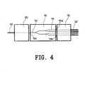
- FIGs. 3 and 4 describe another prior-art-packaged device, which includes a beam splitter 110 and a pair of input and output optical-fiber blocks 120 and 130, each coupled in alignment with the input end and the output end of the beam splitter 110.
- the beam splitter 110 is provided with an input waveguide 112 and a plurality of output waveguides 114 branched out from the input waveguide 112, forming a Y-shaped branched connection of waveguides.
- a single fiber-optic cable 122 is connected to the input optical-fiber block 120, and a ribbon-type fiber-optic cable 132 is connected to the output optical-fiber block 130.
- the beam splitter 110 is also provided with an input port 112a and output ports 114a respectively at both opposite ends, such that the input port 112a is disposed at one end of the beam splitter 110 facing the input optical-fiber block 120, while the output ports 114a are disposed at both opposite ends facing the output optical-fiber block 130.
- Due to the complexity in the structure it is often difficult to precisely align the input and output optical-fiber blocks with respect to the input and output ports of the optical waveguide including the beam splitter. In particular, it requires twice as much time to implement the alignment processes, i.e., first aligning the input optical-fiber block with the planar lightguide circuit and then aligning the output optical-fiber block in a similar manner. As a result, productivity and reliability are compromised.
- the thermal deformation that may occur in the course of bonding the optical elements with any adhesive material or epoxy resin during the alignment process will also produce an adverse effect on reliability.
- the prior-art alignment scheme of the planar lightguide circuit usually requires at least two optical-fiber blocks, spaced apart opposite to each other, such that the total size or volume of the associated optical module is undesirably large.
- the present invention is related to a packaged device for producing a planar light - guide circuit, in which the alignment process time between the planar light-guide circuit and an optical-fiber block is greatly reduced, by arranging an input port and an output port of the planar light-guide circuit on one end of the same surface.
- a packaged device for alignment between a planar lightguide circuit and an optical-fiber block includes: the planar lightguide circuit having an input port of an input waveguide, a plurality of output ports of output waveguides, arranged on the same surface as that of the input port of the input waveguide, and, at least one dummy waveguide arranged abutting the outermost end of the output waveguides; and, an output port of the dummy waveguide being arranged on the same surface, wherein the optical-fiber block has a plurality of ports corresponding to the input port of the input waveguide and the output ports of the output waveguides.
- a packaged device for alignment between a planar lightguide circuit and an optical-fiber block includes: the planar lightguide circuit having an input port of an input waveguide; a plurality of output ports of output waveguides, arranged on the same surface as that of the input port, and at least one aligning waveguide having aligning ports, arranged on the same surface; and, a optical-fiber block having a plurality of ports each corresponding to the input port of the input waveguide, the output ports of the output waveguides, and the aligning port.
- the plurality of ports of the optical-fiber block is respectively coupled in alignment with the input port, the output ports, and the aligning ports.
- a packaged device for manufacturing an optical module of a beam splitter and an optical-fiber block in alignment includes: the beam splitter having an input port of an input waveguide; a plurality of output ports of output waveguides arranged on the same surface as that of the input port, and at least one aligning waveguide having aligning ports arranged on the same surface; and, the optical-fiber block having a plurality of ports each corresponding to the input port of the input waveguide, the output ports of the output waveguides, and the aligning port, wherein the plurality of ports of the optical-fiber block are coupled in alignment with the input port, the output ports, and the aligning ports, respectively.
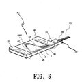
- FIGs. 5 and 6 a packaged device suitable for the planar lightguide circuit 40 according to a first preferred embodiment of the present invention will be described in more detail.
- the packaged device includes the planar lightguide circuit 40 having a set of input/output waveguide ports 41a and 44a disposed apart from each other on the same surface S1, and a single optical-fiber block 50 disposed in alignment with the set of input/output waveguide ports of the planar lightguide circuit 40.
- the single optical-fiber block 50 is fixably attached to each of the input/output waveguide ports of the planar lightguide circuit 40 using an adhesion material or means, such as epoxy resin, thermosetting adhesive, or welding.
- the single optical-fiber block 50 is coupled in alignment with the input port 41a of the input waveguide 41 and the output ports 44a of output waveguide 44 of the planar lightguide circuit 40, respectively.
- the input port 41a and the output ports 44a are formed on the identical edge surface S1 of the planar lightguide circuit 40, and both are disposed in the identical direction.
- the input port 41a of the input waveguide 41 and the output ports 44a of the output waveguide 44 are spaced apart from each other and aligned with the single optical-fiber block 50.
- the planar lightguide circuit 40 is an integrated element formed through a deposition of a multiplicity of thin layers, which consist of silica or polymer on a silicon or quartz substrate, serving as an optical waveguide for guiding the optical signal within a core of the fiber optic based on the difference in the refractive index between the core and its surrounding cladding.
- the input/output waveguide ports 41a and 44a of the planar lightguide circuit 40 are coupled with one end surface of the single optical-fiber block 50 facing each other.
- the planar lightguide circuit 40 is provided with at least one aligning waveguide 45 for carrying out an initial alignment between the arrayed-waveguide-grating AWG1 and the single optical-fiber block 50, by projecting the light beam into the input waveguide 45a and then measuring the optical power via the aligning waveguide 45, and it is further provided with at least one dummy waveguide 46 at both ends of the output waveguide 44.
- the aligning waveguide 45 includes an input-aligning port 45a and an output-aligning port 45b, in which the input-aligning port 45a is coupled in alignment with one end of the single optical-fiber block 50. Note that the output-aligning port 45b is not disposed on the same surface S1 as in the input-aligning input port 45a. The output-aligning port 45b is disposed on the other edge surface S2 opposite to the surface S1, so that the aligning waveguide 45 is constructed in the form of a straight waveguide.
- the input-aligning port 45a is coupled in alignment with one end of the single optical-fiber block 50, facing its ending surface, while the output-aligning port 45b is disposed without facing the other end of the single optical-fiber block 50.
- the input-aligning port 45a is positioned in the outermost end of a multiplicity of ports including the input/output waveguide ports on the edge surface S1.
- At least one aligning waveguide 45 is provided in the form of a straight waveguide on the planar lightguide circuit 40 and at least one dummy waveguide 46 also is provided next to the outermost ones of the output waveguides 44.
- the single optical-fiber block 50 aligned with the planar lightguide circuit 40 is also provided in its one end with a plurality of ports (P) corresponding to the plurality of waveguide ports of 41a, 44a, 45a, and 46a in alignment with them.
- the single optical-fiber block 50 is a block for supporting a ribbon-type fiber-optic cable F3, which is affixed to a V-shaped groove (not shown) formed on a silicon or quartz substrate (S) using the adhesive material (B).
- the adhesive material is omitted in the drawing of FIG 6 not to obscure the understanding of the present invention.
- a light beam incident to the input waveguide 41 through the input port 41a sequentially passes through a light channel consisting of a first star coupler 42, an arrayed-waveguide-grating AWG1, a second star coupler 43, and the output waveguide 44, then outputs through the output port 44a.
- the optical glass of upper plates G5 and G6 may be affixed to the part of the planar lightguide circuit 40 for better workability after arrangement of the aligned ribbon-type fiber-optic cable F3 onto the single optical-fiber block 50, and another glass of upper plate G7 also may be affixed thereto for better workability.
- an optical lens (not shown) may be provided in a position just before the output-aligning waveguide 45b in order to measure the optical power initially to perform the initial alignment. That is, the alignment between the arrayed-waveguide-grating AWG1 and the single optical-fiber block 50 is performed by projecting the light beam into the input waveguide 41 and then by measuring the optical power via the dummy waveguide 46.
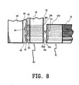
- FIGs. 7 and 8 a packaged device suitable for the planar lightguide circuit 60 according to a second preferred embodiment of the present invention will be described in more detail.
- the packaged device includes a planar lightguide circuit 60 having an input port 61a for the input waveguide 61, a plurality of output ports 64a for the output wave guides 64, an input and output-aligning ports 65a and 65b of an aligning waveguide 65 disposed on the same surface S3 as in the input and output ports 61a and 64a, and a single optical-fiber block 70 disposed in alignment with the planar lightguide circuit 60.
- the single optical-fiber block 70 is provided with a plurality of connection ports P1 to be coupled in alignment with the input port 61a of the input waveguide 61, the output ports 64a for the output waveguides 64, and the input/output-aligning ports 65a and 65b of the aligning waveguide 65 through an adhesive material B2.
- the aligning waveguide 65 is arranged along the optical path and includes a straight waveguide section and a curved waveguide section. Also provided near the aligning waveguide are the input waveguide 61, the output waveguides 64, first and second star couplers 62 and 63, and an arrayed-waveguide-grating AWG2.
- the input/output waveguide ports 61a and 64a and the input/output-aligning ports 65a and 65b of the planar lightguide circuit 60 are coupled in alignment with the plurality of ports on one end surface of the single optical-fiber block 70, facing each other.
- the input/output-aligning ports 65a and 65b are provided for carrying out the initial alignment between the planar lightguide circuit 60 and the single optical-fiber block 70.
- the multiplicity of ports on the surface S3 of the planar lightguide circuit 60 is arranged from the top end in the order of the output-aligning port 65b of the aligning waveguide, the dummy port 66b of a dummy waveguide, the output ports 64a of the output waveguides, a dummy port 66a of the dummy waveguide, the input port 61a of the input waveguide, and the input-aligning port 65a of the aligning waveguide.
- the input-aligning port 65a and the output-aligning port 65b are disposed in both the outermost ends of the arrangement.
- the difference of the second embodiment of the aligning device from the first embodiment is that the output-aligning port 65b of the aligning waveguide is provided on the same surface S3 as in the input-aligning port 65a. Furthermore, it is not limited to use only one aligning waveguide 65 in the present invention, but two or more aligning waveguides may be used.
- the single optical-fiber block 70 is further provided with a fiber-optic cable F4 as well as the plurality of connection ports for coupling in alignment with the corresponding multiplicity of ports of the planar lightguide circuit using the adhesive material.
- the fiber-optic cable F4 may be of a ribbon-type fiber-optic cable with multiple channels, and the planar lightguide circuit 60 may be provided with glass upper plates G8 and G9 affixed thereto using the adhesive material B2 for better workability on manufacturing. Furthermore, another glass upper plate G10 may be bonded to the single optical-fiber block 70 for ensuring better workability by fixing the aligned fiber-optic cable F4.
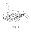
- the aligning device includes a planar lightguide circuit 80 having a plurality of input/output ports 81a and 84a arranged on the same surface S4, and a single optical-fiber block 90 coupled in alignment with a plurality of corresponding waveguides of the planar lightguide circuit 80 using an adhesive means B1, such as epoxy resin, thermosetting bonds, or welding.
- an adhesive means B1 such as epoxy resin, thermosetting bonds, or welding.
- the single optical-fiber block 90 should be coupled in alignment with the input port 81a of the input waveguide 81 and the output ports 84a of the output waveguide 84, respectively.
- the input port 81a and the output ports 84a are designed to form on the same edge surface S4 of the planar lightguide circuit 80, disposed in the identical direction.
- the input port 81a of the input waveguide 81 and the output ports 84a of the output waveguide 84 are disposed, respectively, with a given spacing to each other, in the positions suitable for coupling in alignment with the single optical-fiber block 90.
- An arrayed-waveguide-grating AWG3 formed on the planar lightguide circuit 80 is formed with a deposition of a multiplicity of thin layers, consisting of silica or polymer on a silicon or quartz substrate, for guiding the optical signal within a core of the fiber-optic based on the refractive index difference between the core and its surrounding cladding.
- the input/output waveguide ports 81a and 84a of the planar lightguide circuit 80 are coupled in alignment with one edge surface of the single optical-fiber block 90, facing each other.
- the input port 81a of the input waveguide 81 is disposed between the output ports 84a of the output waveguides 84, so that those output ports 84a are respectively arranged in the outer positions of the input port 81a of the input waveguide 81, with a given spacing to each other.
- the planar lightguide circuit 80 is additionally provided with at least one aligning waveguide 85 for carrying out the initial alignment upon effecting the alignment between the planar lightguide circuit 80 and the single optical-fiber block 90, and it is further provided with at least one dummy waveguide 86 in both ending sides of the output waveguide 84, so as to construct a vernier-type of waveguide elements.
- the aligning waveguide 85 further includes an input-aligning port 85a and an output-aligning port 85b on the same surface S4.
- the aligning waveguide 85 consists of two types of waveguide sections, i.e., a straight waveguide and a curved waveguide.
- the input-aligning port 85a and the output-aligning port 85b are coupled in alignment with one end of the single optical-fiber block 90, facing its ending surface, and the input and output-aligning ports 85a and 85b are respectively positioned next to both outermost ends of the multiplicity of ports arranged on the edge surface S4.
- the planar lightguide circuit 80 may be provided with one or more aligning waveguides 85 as required and also may be provided with one or more dummy waveguides 86 next to the outermost one of the output waveguides 84.
- the planar lightguide circuit 80 functions as an optical component for multiplexing the optical signal, including the input waveguide 81 for receiving the input light beam, a first star coupler 82, an arrayed-waveguide-grating AWG3, a second star coupler 83, and the output waveguides 84.
- the input waveguide 81 is disposed between the output waveguides 84 in parallel thereto.
- the structure and operation of the arrayed waveguide grating and the first and second star couplers 82 and 83 will be well understood to those skilled in the art, so any detailed description thereto is omitted here.
- the single optical-fiber block 90 aligned with the planar lightguide circuit 80 is also provided, in its proximal end, with a plurality of associated ports (P2) to be coupled in alignment with the plurality of waveguide ports of 81a, 84a, 85a, 85b, 86a, and 86b through an adhesive means B3.
- the single optical-fiber block 90 serves as a block for supporting a ribbon-type fiber-optic cable F5, which is affixed to a V-shaped groove (not shown) formed on a silicon or quartz substrate (S) using the adhesive means B3.
- the adhesive means is omitted in the drawing of FIG .10 for the better understanding of the invention.
- a light beam i.e., the optical carrier signal
- incident upon the input waveguide 81 through the input port 81a sequentially passes through an optical channel consisting of the first star coupler 82, the arrayed-waveguide-grating AWG3, the second star coupler 83, and the output waveguide 84, and then outputted through the output port 84a.
- the upper plates G11 and G12 of optical glass may be additionally provided to cover at least a part of the planar lightguide circuit 80, for better workability on manufacturing, and another upper plate G13 of optical glass may be further provided to cover at least a part of the optical-fiber block 90 for better workability by fixing the aligned fiber-optic cable F3 onto the optical-fiber block 90.
- an optical lens (not shown) may be provided in a position just before the output-aligning waveguide 85b in order to measure the optical power and then carry out the initial alignment for the single optical-fiber block 90. In this way, the alignment between the arrayed-waveguide-grating AWG3 and the single optical-fiber block 90 can be carried out by projecting the light beam into the input waveguide 81 and then measuring the optical power in the dummy waveguide 86.
- FIGs. 11 and 12 a packaged device comprised of a beam splitter 210 and a single optical-fiber block 220 according to a fourth preferred embodiment of the present invention will be described.
- the beam splitter 210 includes an input port 210a and a plurality of output ports 210b arranged on the same surface S5 and spaced apart from each other with a given gap, and a single optical-fiber block 220 coupled in alignment with the surface S5 of the beam splitter using the adhesive means B1, such as epoxy resin, thermosetting bonds, or welding.
- the single optical-fiber block 220 is coupled in alignment with the input port 210a of input waveguide 212 and the output ports 210b of output waveguide 214, respectively.
- These input port 210a and the output ports 210b are formed on the same edge surface S5 of the beam splitter 210, disposed in the identical direction.
- the input port 210a of the input waveguide 212 and the output ports 210b of output waveguide 214 of the beam splitter 210 are spaced apart by a given spacing between them, in the position suitable for coupling in alignment with the single optical-fiber block 220, more particularly, on the edge coupling surface S5 facing the single optical-fiber block 220.
- the beam splitter 210 may be preferably provided with at least one aligning waveguide 216 for carrying out the initial alignment between both of them.
- the aligning waveguide 216 includes an input-aligning port 210c and an output-aligning port 210d, in which the input-aligning port 210c is coupled in alignment with one end of the single optical-fiber block 220, while the output-aligning port 210d is not disposed on the same surface S5 as in the input-aligning input port 210c.
- the output-aligning port 210d is disposed on the other edge surface S6 opposite to the surface S5, such that the aligning waveguide 216 is configured in the form of a straight waveguide provided with the input and output-aligning ports 210c and 210d in its opposite edge surfaces, respectively. Accordingly, the input-aligning port 210c is disposed in the outermost end of those ports on the coupling surface S5.
- the single optical-fiber block 220 aligned with the beam splitter 210 is also provided in its one end with a plurality of ports 220a matching the plurality of waveguide ports of 210a, 210b, and 210c.
- a light beam i.e., the optical signal incident upon the input waveguide 212 via the input port 210a, is transferred along the optical path to the output ports 210b through the output waveguide 214.
- the present invention makes it possible to achieve the alignment between a planar lightguide circuit and an optical-fiber block simply by arranging the input/output ports of the planar lightguide circuit at one end of the surface.
- the alignment between the planar lightguide circuit and the single optical block according to the present invention allows the size of an optical communication module to be greatly reduced, by coupling the input/out ports of the input and output waveguides with the single optical block in alignment with the same. Furthermore, such a single process of alignment between the planar lightguide circuit and the single optical block according to the present invention will lead to a reduced alignment time on manufacturing the planar lightguide circuit.
Landscapes
- Physics & Mathematics (AREA)
- General Physics & Mathematics (AREA)
- Optics & Photonics (AREA)
- Engineering & Computer Science (AREA)
- Microelectronics & Electronic Packaging (AREA)
- Optical Couplings Of Light Guides (AREA)
- Optical Integrated Circuits (AREA)
Abstract
Description
- The present invention generally relates to a planar lightguide circuit (PLC) for use in wavelength-division multiplexing/demultiplexing optical communication systems and, in particular, to a packaged device for an alignment between a planar lightguide circuit and an optical-fiber block to produce a combined single module.
- In general, a wavelength-division-multiplexing (WDM) communication system involves transfers of multiple wavelengths of optical signals on a single strand of fiber. At the receiving ends, the optical signal received is divided into a plurality of optical signals with a respective wavelength and then converted into electrical signals. To this end, an arrayed-waveguide-grating (AWG) is mainly utilized in the receiving ends to effect such division of the optical signal into multiple wavelengths.
- Recently, much research has been focused in the field of optical communication, in particular, on the integration of planar-lightguide-circuit (PLC) elements for forming an optical-waveguide element on a planar substrate. As such, the PLC is used for processing optical signals in a variety of operations, such as branching, modulation, switching, or multiplexing/demultiplexing of the optical signals. The PLC incorporates optical waveguides, which are used for propagating optical signals along the length, i.e., in the longitudinal direction, of an optical-fiber cable. The optical waveguides, consisting of a core member with a high refractive index and a cladding member with a low refractive index, are typically formed by multiple thin layers of silica or polymer on the silicon or quartz substrate and serve various functions such as splitting an optical signal, changing its path or adjusting its light intensity based on the difference in the refractive index between the core and its surrounding cladding.
- Referring to FIGs. 1 and 2, a prior-art packaged device for fabricating a planar-light-guide-circuit (PLC) 10 will be explained hereinafter. For simplicity and clarity, a discussion pertaining to well-known components of the PLC and an adhesion means (B) in FIG 2 is omitted. As shown in FIGs. 1 and 2, the
PLC element 10 includes a set of aligned optical-fiber blocks fiber block 20 and the output optical-fiber block 30 are positioned in alignment with an input port 12a and output ports 18a of thePLC 10, respectively, for supporting the optical-fiber cables (a single fiber-optic cable F1 or a ribbon-type, fiber-optic cable F2). The optical cables are generally disposed in a V-shaped groove (not shown) formed on a silicon substrate and fixed to the input port 12a and the output ports 18a of thePLC 10 by an adhesion material (B), i.e., epoxy resins. ThePLC 10 operates to multiplex wavelengths, in which a multiple wavelength signal is inputted into aninput waveguide 12 and the respective multiplexed wavelength appears at eachoutput waveguide 18. ThePLC 10 further includes aninput waveguide 12 provided before an arrayed waveguide grating (AWG) and anoutput waveguides 18 provided after the arrayed waveguide grating in opposite end. Afirst start coupler 14 and asecond star coupler 16 are disposed between the input waveguide and the output waveguides before and after the arrayed waveguide grating. - The prior-art packaged device as described above is configured so that the input optical-
fiber block 20 is in alignment with and fixed to the input port 12a of the input waveguide using a precise position-control device (not shown). Similarly, the output optical-fiber block 30 is in alignment with and fixed to the output ports 18a of the output waveguides using the same positioning device. Both blocks are then sealed into a housing (not shown) to complete the packaging. As such, multiple optical signals received by the single fiber-optic cable F1 and pass through, sequentially, the input port 12a,input waveguide 12,first star coupler 14, arrayed-waveguide-grating (AWG),second star coupler 16,output waveguides 18, and output ports 18a, toward the ribbon-type fiber-optic cable F2. Furthermore, glass upper plates G1 to G4 are provided to enhance the stability of those components, such as thePLC 10, the input or output optical-fiber blocks fiber blocks - FIGs. 3 and 4 describe another prior-art-packaged device, which includes a
beam splitter 110 and a pair of input and output optical-fiber blocks beam splitter 110. Thebeam splitter 110 is provided with aninput waveguide 112 and a plurality ofoutput waveguides 114 branched out from theinput waveguide 112, forming a Y-shaped branched connection of waveguides. A single fiber-optic cable 122 is connected to the input optical-fiber block 120, and a ribbon-type fiber-optic cable 132 is connected to the output optical-fiber block 130. Thebeam splitter 110 is also provided with aninput port 112a andoutput ports 114a respectively at both opposite ends, such that theinput port 112a is disposed at one end of thebeam splitter 110 facing the input optical-fiber block 120, while theoutput ports 114a are disposed at both opposite ends facing the output optical-fiber block 130. Due to the complexity in the structure, it is often difficult to precisely align the input and output optical-fiber blocks with respect to the input and output ports of the optical waveguide including the beam splitter. In particular, it requires twice as much time to implement the alignment processes, i.e., first aligning the input optical-fiber block with the planar lightguide circuit and then aligning the output optical-fiber block in a similar manner. As a result, productivity and reliability are compromised. In addition, the thermal deformation that may occur in the course of bonding the optical elements with any adhesive material or epoxy resin during the alignment process will also produce an adverse effect on reliability. Furthermore, the prior-art alignment scheme of the planar lightguide circuit usually requires at least two optical-fiber blocks, spaced apart opposite to each other, such that the total size or volume of the associated optical module is undesirably large. - The present invention is related to a packaged device for producing a planar light - guide circuit, in which the alignment process time between the planar light-guide circuit and an optical-fiber block is greatly reduced, by arranging an input port and an output port of the planar light-guide circuit on one end of the same surface.
- It is an object of the present invention to provide a packaged device for a planar lightguide circuit having a structure more suitable for miniaturization and simplification of its structure.
- It is another object of the present invention to provide a packaged device for a planar lightguide circuit having a structure more suitable for reduction in the production cost.
- According to one aspect of the invention, a packaged device for alignment between a planar lightguide circuit and an optical-fiber block includes: the planar lightguide circuit having an input port of an input waveguide, a plurality of output ports of output waveguides, arranged on the same surface as that of the input port of the input waveguide, and, at least one dummy waveguide arranged abutting the outermost end of the output waveguides; and, an output port of the dummy waveguide being arranged on the same surface, wherein the optical-fiber block has a plurality of ports corresponding to the input port of the input waveguide and the output ports of the output waveguides.
- According to another aspect of the present invention, a packaged device for alignment between a planar lightguide circuit and an optical-fiber block includes: the planar lightguide circuit having an input port of an input waveguide; a plurality of output ports of output waveguides, arranged on the same surface as that of the input port, and at least one aligning waveguide having aligning ports, arranged on the same surface; and, a optical-fiber block having a plurality of ports each corresponding to the input port of the input waveguide, the output ports of the output waveguides, and the aligning port. The plurality of ports of the optical-fiber block is respectively coupled in alignment with the input port, the output ports, and the aligning ports.
- According to a further aspect of the present invention, a packaged device for manufacturing an optical module of a beam splitter and an optical-fiber block in alignment includes: the beam splitter having an input port of an input waveguide; a plurality of output ports of output waveguides arranged on the same surface as that of the input port, and at least one aligning waveguide having aligning ports arranged on the same surface; and, the optical-fiber block having a plurality of ports each corresponding to the input port of the input waveguide, the output ports of the output waveguides, and the aligning port, wherein the plurality of ports of the optical-fiber block are coupled in alignment with the input port, the output ports, and the aligning ports, respectively.
- The above and other features and advantages of the present invention will become more apparent from the following detailed description when taken in conjunction with the accompanying drawings in which:
- FIG 1 is a schematic, partially enlarged, perspective view of a packaged device for a planar lightguide circuit according to a prior art;
- FIG 2 is a schematic, partially enlarged, planar view of an aligned section between the planar lightguide circuit and its input/output optical-fiber blocks according to the prior art;
- FIG 3 is a schematic, partially enlarged, perspective view of a packaged device between a beam splitter and its input/output optical-fiber blocks according to another prior art;
- FIG 4 is a schematic, partially enlarged, planar view of an aligned section between a beam splitter and its input/output optical-fiber blocks according to the prior art;
- FIG 5 is a schematic, partially enlarged, perspective view of a packaged device for a planar lightguide circuit according to a first preferred embodiment of the present invention;
- FIG 6 is a schematic, partially enlarged, planar view of an aligned portion between a planar lightguide circuit and a single optical-fiber block according to the first preferred embodiment of the present invention;
- FIG 7 is a schematic, partially enlarged, perspective view of a packaged device for a planar lightguide circuit according to a second preferred embodiment of the present invention;
- FIG 8 is a schematic, partially enlarged, planar view of an aligned portion between a planar lightguide circuit and a single optical-fiber block according to the second preferred embodiment of the present invention;
- FIG 9 is a schematic, partially enlarged, perspective view of a packaged device for a planar lightguide circuit according to a third preferred embodiment of the present invention;
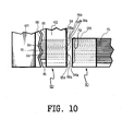
- FIG 10 is a schematic, partially enlarged, planar view of an aligned portion between a planar lightguide circuit and a single optical-fiber block according to the third preferred embodiment of the present invention;
- FIG 11 is a schematic, partially enlarged, perspective view of a packaged device for a beam splitter and a single optical-fiber block according to a fourth preferred embodiment of the present invention; and,
- FIG 12 is a schematic, partially enlarged, planar view of an aligned portion between a beam splitter and a single optical-fiber block according to the fourth preferred embodiment of the present invention.
- In the following description, for purposes of explanation rather than limitation, specific details are set forth such as the particular architecture, interfaces, techniques, etc., in order to provide a thorough understanding of the present invention. However, it will be apparent to those skilled in the art that the present invention may be practiced in other embodiments, which depart from these specific details. For purposes of simplicity and clarity, detailed descriptions of well-known devices, circuits, and methods are omitted so as not to obscure the description of the present invention with unnecessary detail.
- Referring now to FIGs. 5 and 6, a packaged device suitable for the
planar lightguide circuit 40 according to a first preferred embodiment of the present invention will be described in more detail. - The packaged device according to the first preferred embodiment includes the
planar lightguide circuit 40 having a set of input/output waveguide ports 41a and 44a disposed apart from each other on the same surface S1, and a single optical-fiber block 50 disposed in alignment with the set of input/output waveguide ports of theplanar lightguide circuit 40. The single optical-fiber block 50 is fixably attached to each of the input/output waveguide ports of theplanar lightguide circuit 40 using an adhesion material or means, such as epoxy resin, thermosetting adhesive, or welding. The single optical-fiber block 50 is coupled in alignment with theinput port 41a of theinput waveguide 41 and the output ports 44a ofoutput waveguide 44 of theplanar lightguide circuit 40, respectively. Theinput port 41a and the output ports 44a are formed on the identical edge surface S1 of theplanar lightguide circuit 40, and both are disposed in the identical direction. Preferably, theinput port 41a of theinput waveguide 41 and the output ports 44a of theoutput waveguide 44 are spaced apart from each other and aligned with the single optical-fiber block 50. - The
planar lightguide circuit 40 is an integrated element formed through a deposition of a multiplicity of thin layers, which consist of silica or polymer on a silicon or quartz substrate, serving as an optical waveguide for guiding the optical signal within a core of the fiber optic based on the difference in the refractive index between the core and its surrounding cladding. - In alignment between the
planar lightguide circuit 40 and the single optical-fiber block 50, the input/output waveguide ports 41a and 44a of theplanar lightguide circuit 40 are coupled with one end surface of the single optical-fiber block 50 facing each other. Preferably, theplanar lightguide circuit 40 is provided with at least one aligningwaveguide 45 for carrying out an initial alignment between the arrayed-waveguide-grating AWG1 and the single optical-fiber block 50, by projecting the light beam into theinput waveguide 45a and then measuring the optical power via the aligningwaveguide 45, and it is further provided with at least onedummy waveguide 46 at both ends of theoutput waveguide 44. - The aligning
waveguide 45 includes an input-aligningport 45a and an output-aligningport 45b, in which the input-aligningport 45a is coupled in alignment with one end of the single optical-fiber block 50. Note that the output-aligningport 45b is not disposed on the same surface S1 as in the input-aligninginput port 45a. The output-aligningport 45b is disposed on the other edge surface S2 opposite to the surface S1, so that the aligningwaveguide 45 is constructed in the form of a straight waveguide. Accordingly, the input-aligningport 45a is coupled in alignment with one end of the single optical-fiber block 50, facing its ending surface, while the output-aligningport 45b is disposed without facing the other end of the single optical-fiber block 50. The input-aligningport 45a is positioned in the outermost end of a multiplicity of ports including the input/output waveguide ports on the edge surface S1. - Preferably, at least one aligning
waveguide 45 is provided in the form of a straight waveguide on theplanar lightguide circuit 40 and at least onedummy waveguide 46 also is provided next to the outermost ones of theoutput waveguides 44. In the meantime, the single optical-fiber block 50 aligned with theplanar lightguide circuit 40 is also provided in its one end with a plurality of ports (P) corresponding to the plurality of waveguide ports of 41a, 44a, 45a, and 46a in alignment with them. The single optical-fiber block 50 is a block for supporting a ribbon-type fiber-optic cable F3, which is affixed to a V-shaped groove (not shown) formed on a silicon or quartz substrate (S) using the adhesive material (B). For the purpose of clarity and simplicity, the adhesive material is omitted in the drawing of FIG 6 not to obscure the understanding of the present invention. - According to the foregoing description of the first preferred embodiment, a light beam incident to the
input waveguide 41 through theinput port 41a sequentially passes through a light channel consisting of afirst star coupler 42, an arrayed-waveguide-grating AWG1, asecond star coupler 43, and theoutput waveguide 44, then outputs through the output port 44a. - Preferably, the optical glass of upper plates G5 and G6 may be affixed to the part of the
planar lightguide circuit 40 for better workability after arrangement of the aligned ribbon-type fiber-optic cable F3 onto the single optical-fiber block 50, and another glass of upper plate G7 also may be affixed thereto for better workability. Furthermore, an optical lens (not shown) may be provided in a position just before the output-aligningwaveguide 45b in order to measure the optical power initially to perform the initial alignment. That is, the alignment between the arrayed-waveguide-grating AWG1 and the single optical-fiber block 50 is performed by projecting the light beam into theinput waveguide 41 and then by measuring the optical power via thedummy waveguide 46. - Referring now to FIGs. 7 and 8, a packaged device suitable for the
planar lightguide circuit 60 according to a second preferred embodiment of the present invention will be described in more detail. - The packaged device according to the second preferred embodiment includes a
planar lightguide circuit 60 having aninput port 61a for theinput waveguide 61, a plurality of output ports 64a for the output wave guides 64, an input and output-aligningports 65a and 65b of an aligningwaveguide 65 disposed on the same surface S3 as in the input andoutput ports 61a and 64a, and a single optical-fiber block 70 disposed in alignment with theplanar lightguide circuit 60. The single optical-fiber block 70 is provided with a plurality of connection ports P1 to be coupled in alignment with theinput port 61a of theinput waveguide 61, the output ports 64a for theoutput waveguides 64, and the input/output-aligningports 65a and 65b of the aligningwaveguide 65 through an adhesive material B2. The aligningwaveguide 65 is arranged along the optical path and includes a straight waveguide section and a curved waveguide section. Also provided near the aligning waveguide are theinput waveguide 61, theoutput waveguides 64, first andsecond star couplers - In the alignment between the
planar lightguide circuit 60 and the single optical-fiber block 70, the input/output waveguide ports 61a and 64a and the input/output-aligningports 65a and 65b of theplanar lightguide circuit 60 are coupled in alignment with the plurality of ports on one end surface of the single optical-fiber block 70, facing each other. The input/output-aligningports 65a and 65b are provided for carrying out the initial alignment between theplanar lightguide circuit 60 and the single optical-fiber block 70. - The multiplicity of ports on the surface S3 of the
planar lightguide circuit 60 is arranged from the top end in the order of the output-aligning port 65b of the aligning waveguide, the dummy port 66b of a dummy waveguide, the output ports 64a of the output waveguides, adummy port 66a of the dummy waveguide, theinput port 61a of the input waveguide, and the input-aligningport 65a of the aligning waveguide. In particular, the input-aligningport 65a and the output-aligning port 65b are disposed in both the outermost ends of the arrangement. - As a result, the difference of the second embodiment of the aligning device from the first embodiment is that the output-aligning port 65b of the aligning waveguide is provided on the same surface S3 as in the input-aligning
port 65a. Furthermore, it is not limited to use only one aligningwaveguide 65 in the present invention, but two or more aligning waveguides may be used. The single optical-fiber block 70 is further provided with a fiber-optic cable F4 as well as the plurality of connection ports for coupling in alignment with the corresponding multiplicity of ports of the planar lightguide circuit using the adhesive material. Preferably, the fiber-optic cable F4 may be of a ribbon-type fiber-optic cable with multiple channels, and theplanar lightguide circuit 60 may be provided with glass upper plates G8 and G9 affixed thereto using the adhesive material B2 for better workability on manufacturing. Furthermore, another glass upper plate G10 may be bonded to the single optical-fiber block 70 for ensuring better workability by fixing the aligned fiber-optic cable F4. - Referring to FIGs. 9 and 10, the aligning device according to a third embodiment of the present invention includes a planar lightguide circuit 80 having a plurality of input/
output ports 81a and 84a arranged on the same surface S4, and a single optical-fiber block 90 coupled in alignment with a plurality of corresponding waveguides of the planar lightguide circuit 80 using an adhesive means B1, such as epoxy resin, thermosetting bonds, or welding. - The single optical-
fiber block 90 should be coupled in alignment with theinput port 81a of theinput waveguide 81 and the output ports 84a of theoutput waveguide 84, respectively. Theinput port 81a and the output ports 84a are designed to form on the same edge surface S4 of the planar lightguide circuit 80, disposed in the identical direction. Preferably, theinput port 81a of theinput waveguide 81 and the output ports 84a of theoutput waveguide 84 are disposed, respectively, with a given spacing to each other, in the positions suitable for coupling in alignment with the single optical-fiber block 90. - An arrayed-waveguide-grating AWG3 formed on the planar lightguide circuit 80 is formed with a deposition of a multiplicity of thin layers, consisting of silica or polymer on a silicon or quartz substrate, for guiding the optical signal within a core of the fiber-optic based on the refractive index difference between the core and its surrounding cladding.
- In alignment between the planar lightguide circuit 80 and the single optical-
fiber block 90, the input/output waveguide ports 81a and 84a of the planar lightguide circuit 80 are coupled in alignment with one edge surface of the single optical-fiber block 90, facing each other. Theinput port 81a of theinput waveguide 81 is disposed between the output ports 84a of theoutput waveguides 84, so that those output ports 84a are respectively arranged in the outer positions of theinput port 81a of theinput waveguide 81, with a given spacing to each other. Preferably, the planar lightguide circuit 80 is additionally provided with at least one aligningwaveguide 85 for carrying out the initial alignment upon effecting the alignment between the planar lightguide circuit 80 and the single optical-fiber block 90, and it is further provided with at least onedummy waveguide 86 in both ending sides of theoutput waveguide 84, so as to construct a vernier-type of waveguide elements. - The aligning
waveguide 85 further includes an input-aligningport 85a and an output-aligning port 85b on the same surface S4. The aligningwaveguide 85 consists of two types of waveguide sections, i.e., a straight waveguide and a curved waveguide. The input-aligningport 85a and the output-aligning port 85b are coupled in alignment with one end of the single optical-fiber block 90, facing its ending surface, and the input and output-aligningports 85a and 85b are respectively positioned next to both outermost ends of the multiplicity of ports arranged on the edge surface S4. - Preferably, the planar lightguide circuit 80 may be provided with one or more aligning
waveguides 85 as required and also may be provided with one ormore dummy waveguides 86 next to the outermost one of theoutput waveguides 84. The planar lightguide circuit 80 functions as an optical component for multiplexing the optical signal, including theinput waveguide 81 for receiving the input light beam, a first star coupler 82, an arrayed-waveguide-grating AWG3, asecond star coupler 83, and theoutput waveguides 84. Theinput waveguide 81 is disposed between theoutput waveguides 84 in parallel thereto. The structure and operation of the arrayed waveguide grating and the first andsecond star couplers 82 and 83 will be well understood to those skilled in the art, so any detailed description thereto is omitted here. - In the meantime, the single optical-
fiber block 90 aligned with the planar lightguide circuit 80 is also provided, in its proximal end, with a plurality of associated ports (P2) to be coupled in alignment with the plurality of waveguide ports of 81a, 84a, 85a, 85b, 86a, and 86b through an adhesive means B3. The single optical-fiber block 90 serves as a block for supporting a ribbon-type fiber-optic cable F5, which is affixed to a V-shaped groove (not shown) formed on a silicon or quartz substrate (S) using the adhesive means B3. The adhesive means is omitted in the drawing of FIG .10 for the better understanding of the invention. Therefore, according to the above description of the preferred embodiment, a light beam, i.e., the optical carrier signal, incident upon theinput waveguide 81 through theinput port 81a sequentially passes through an optical channel consisting of the first star coupler 82, the arrayed-waveguide-grating AWG3, thesecond star coupler 83, and theoutput waveguide 84, and then outputted through the output port 84a. - Preferably, the upper plates G11 and G12 of optical glass may be additionally provided to cover at least a part of the planar lightguide circuit 80, for better workability on manufacturing, and another upper plate G13 of optical glass may be further provided to cover at least a part of the optical-
fiber block 90 for better workability by fixing the aligned fiber-optic cable F3 onto the optical-fiber block 90. Further, an optical lens (not shown) may be provided in a position just before the output-aligning waveguide 85b in order to measure the optical power and then carry out the initial alignment for the single optical-fiber block 90. In this way, the alignment between the arrayed-waveguide-grating AWG3 and the single optical-fiber block 90 can be carried out by projecting the light beam into theinput waveguide 81 and then measuring the optical power in thedummy waveguide 86. - Referring now to FIGs. 11 and 12, a packaged device comprised of a
beam splitter 210 and a single optical-fiber block 220 according to a fourth preferred embodiment of the present invention will be described. - The
beam splitter 210 includes aninput port 210a and a plurality ofoutput ports 210b arranged on the same surface S5 and spaced apart from each other with a given gap, and a single optical-fiber block 220 coupled in alignment with the surface S5 of the beam splitter using the adhesive means B1, such as epoxy resin, thermosetting bonds, or welding. The single optical-fiber block 220 is coupled in alignment with theinput port 210a ofinput waveguide 212 and theoutput ports 210b ofoutput waveguide 214, respectively. Theseinput port 210a and theoutput ports 210b are formed on the same edge surface S5 of thebeam splitter 210, disposed in the identical direction. Preferably, theinput port 210a of theinput waveguide 212 and theoutput ports 210b ofoutput waveguide 214 of thebeam splitter 210 are spaced apart by a given spacing between them, in the position suitable for coupling in alignment with the single optical-fiber block 220, more particularly, on the edge coupling surface S5 facing the single optical-fiber block 220. Furthermore, in the alignment between thebeam splitter 210 and the single optical-fiber block 220, thebeam splitter 210 may be preferably provided with at least one aligningwaveguide 216 for carrying out the initial alignment between both of them. - The aligning
waveguide 216 includes an input-aligningport 210c and an output-aligningport 210d, in which the input-aligningport 210c is coupled in alignment with one end of the single optical-fiber block 220, while the output-aligningport 210d is not disposed on the same surface S5 as in the input-aligninginput port 210c. The output-aligningport 210d, however, is disposed on the other edge surface S6 opposite to the surface S5, such that the aligningwaveguide 216 is configured in the form of a straight waveguide provided with the input and output-aligningports port 210c is disposed in the outermost end of those ports on the coupling surface S5. - The single optical-
fiber block 220 aligned with thebeam splitter 210 is also provided in its one end with a plurality ofports 220a matching the plurality of waveguide ports of 210a, 210b, and 210c. According to the above structure of the beam splitter, a light beam, i.e., the optical signal incident upon theinput waveguide 212 via theinput port 210a, is transferred along the optical path to theoutput ports 210b through theoutput waveguide 214. As a result, the present invention makes it possible to achieve the alignment between a planar lightguide circuit and an optical-fiber block simply by arranging the input/output ports of the planar lightguide circuit at one end of the surface. - As apparent from the foregoing description, it will be understood that the alignment between the planar lightguide circuit and the single optical block according to the present invention allows the size of an optical communication module to be greatly reduced, by coupling the input/out ports of the input and output waveguides with the single optical block in alignment with the same. Furthermore, such a single process of alignment between the planar lightguide circuit and the single optical block according to the present invention will lead to a reduced alignment time on manufacturing the planar lightguide circuit.
- While the invention has been shown and described with reference to a certain preferred embodiment thereof, it will be understood by those skilled in the art that various changes in form and details may be made therein without departing from the spirit and scope of the invention as defined by the appended claims.
Claims (19)
- A packaged device for an alignment between a planar lightguide circuit (40,60,80,210) and an optical-fiber block (50,70,90,220), comprising:said planar lightguide circuit (40,60,80,210) comprising;an input port (41a,61a,81a,210a) of an input waveguide (41,61,81,212),a plurality of output ports (44a,64a,84a,210b) of output waveguides (44,64,84,214), arranged on the same surface (S1) as said input port (41a,61a,81a,210a) of the input waveguide (41,61,81,212), and,said optical-fiber block (50,70,90,220) comprising a plurality of ports corresponding to said input port (41a,61a,81a,210a) of the input waveguide (41,61,81,212) and said output ports (44a,64a,84a,210b) of the output waveguides (44,64,84,214), said optical-fiber block (50,70,90,220) being coupled in alignment with said input port (41a,61a,81a,210a) of the input waveguide (41,61,81,212) and said output ports (44a,64a,84a,210b) of the output waveguides (44,64,84,214).
- The packaged device according to claim 1, wherein said output waveguide (44,64,84,214) comprises a dummy waveguide (46,66,86).
- The packaged device according to claim 2, wherein said dummy waveguide (46,66,86) is disposed in proximity to the outermost end of said output waveguides (44,64,84,214).
- The packaged device according to claim 1, comprising at least one dummy waveguide (46,66,86) is arranged abutting the outermost end of said output waveguides (44,64,84,214), an output port (44a,64a,84a,210b) of said dummy waveguide (46,66,86) being arranged in the same surface (S1);
- The packaged device according to any of claims 1 to 4, wherein said planar lightguide circuit (40,60,80,210) further comprises at least one aligning waveguide (45,65,85,216) for carrying out an initial alignment.
- The packaged device according to claim 5, wherein said aligning waveguide (45,65,85,216) is used to measure the intensity of the optical power of an optical signal with an optical-measuring device.
- The packaged device according to claim 5 or 6, wherein said aligning waveguide (45,65,85,216) comprises an input-aligning port (45a,65a,85a,210c) and an output-aligning port (45b,65b,85b,210d).
- The packaged device according to claim 7, wherein said input-aligning port (45a,65a,85a,210c) is arranged on said same surface (S1).
- The packaged device according to any one of claims 5 to 8, wherein said aligning waveguide (45,65,85,216) comprises a straight waveguide.
- The packaged device according to any one of claims 5 to 9, wherein said aligning waveguide (45,65,85,216) is disposed substantially in line with said output waveguides (44,64,84,214), and comprises a straight waveguide section in close proximity to the outermost one of said output waveguides (44,64,84,214).
- The packaged device according to claim 5 to 9, wherein said aligning waveguide (45,65,85,216) is disposed in line with said input waveguide (41,61,81,212), in close proximity to said input waveguide (41,61,81,212).
- The packaged device according to claim 5 to 9, wherein said aligning waveguide (45,65,85,216) is disposed in line with said input and output waveguides (41,61,81,212,44,64,84,214), in close proximity to said input and output waveguides (41,61,81,212,44,64,84,214).
- The packaged device according to any of claims 7 to 12, wherein said output-aligning port (45b,65b,85b,210d) of said aligning waveguide (45,65,85,216) is arranged on a different surface other than said same surface (S1).
- The packaged device according to any of claims 7 to 12, wherein both of said input-aligning port (45a,65a,85a,210c) and said output-aligning port (45b,65b,85b,210d) are arranged on the same surface (S1).
- The packaged device according to any one of claims 7 to 14 wherein
said plurality of ports of said optical-fiber block (50,70,90,220) correspond to said input port (41a,61a,81a,210a) of the input waveguide (41,61,81,212), said output ports (44a,64a,84a,210b) of the output waveguides (44,64,84,214), and said aligning port (45a,65a,85a,210c,45b,65b,85b,210d), said plurality of ports of said optical-fiber block (50,70,90,220) being coupled in alignment with said input port (41a,61a,81a,210a), said output ports (44a,64a,84a,210b) and said aligning ports (45a,65a,85a,210c,45b,65b,85b,210d), respectively. - The packaged device according to claim 7 to 15, wherein said input-aligning port (45a,65a,85a,210c) and said output-aligning port (45b,65b,85b,210d) are arranged, spaced apart from each other, in proximity to the outermost end of said output waveguide(44,64,84,214).
- The packaged device according to claim 4 to 16, wherein said aligning waveguide (45,65,85,216) comprises a straight waveguide section and a curved waveguide section.
- The packaged device according to any of claims 1 to 17, wherein said input port (41a,61a,81a,210a) of said input waveguide (41,61,81,212) is arranged between said output ports (44a,64a,84a,210b) of said output waveguides (44,64,84,214).
- A packaged device according to any of claims 1 to 18 wherein the planar lightguide circuit (40,60,80,210) is an optical beam splitter (210) and the packaged device is a device for manufacturing an optical module of a beam splitter (210) and an optical-fiber block (50,70,90,220) in alignment
Applications Claiming Priority (2)
| Application Number | Priority Date | Filing Date | Title |
|---|---|---|---|
| KR10-2001-0044380A KR100389837B1 (en) | 2001-07-24 | 2001-07-24 | Packaging device for waveguide element |
| KR2001044380 | 2001-07-24 |
Publications (2)
| Publication Number | Publication Date |
|---|---|
| EP1279979A2 true EP1279979A2 (en) | 2003-01-29 |
| EP1279979A3 EP1279979A3 (en) | 2004-06-16 |
Family
ID=19712459
Family Applications (1)
| Application Number | Title | Priority Date | Filing Date |
|---|---|---|---|
| EP02009778A Withdrawn EP1279979A3 (en) | 2001-07-24 | 2002-04-30 | Packaged device for optical waveguide element |
Country Status (4)
| Country | Link |
|---|---|
| US (1) | US6839492B2 (en) |
| EP (1) | EP1279979A3 (en) |
| JP (1) | JP2003057487A (en) |
| KR (1) | KR100389837B1 (en) |
Cited By (1)
| Publication number | Priority date | Publication date | Assignee | Title |
|---|---|---|---|---|
| EP1780565A3 (en) * | 2005-10-11 | 2007-05-16 | Rohm and Haas Electronic Materials, L.L.C. | Micro-optical device with a U-shaped type alignment waveguide |
Families Citing this family (45)
| Publication number | Priority date | Publication date | Assignee | Title |
|---|---|---|---|---|
| US20040028348A1 (en) * | 2002-03-15 | 2004-02-12 | Marie-Claude Cote | Method and apparatus for assembling optical devices |
| AU2003227262A1 (en) * | 2002-03-28 | 2003-10-13 | Hitachi Chemical Co., Ltd. | Optical waveguide and optical multiplexer/demultiplexer |
| KR100442657B1 (en) * | 2002-03-29 | 2004-08-02 | 삼성전자주식회사 | Wavelength division multiplexer with arrayed waveguide grating |
| KR100421137B1 (en) * | 2002-03-30 | 2004-03-04 | 삼성전자주식회사 | Dual wavelength division multiplexing/demultiplexing device using one planar lightguide circuit |
| WO2009063986A1 (en) * | 2007-11-15 | 2009-05-22 | Nippon Telegraph And Telephone Corporation | Optical circuit and optical signal processing device using the same |
| US8452148B2 (en) | 2008-08-29 | 2013-05-28 | Corning Cable Systems Llc | Independently translatable modules and fiber optic equipment trays in fiber optic equipment |
| US11294136B2 (en) | 2008-08-29 | 2022-04-05 | Corning Optical Communications LLC | High density and bandwidth fiber optic apparatuses and related equipment and methods |
| ATE534049T1 (en) | 2009-02-24 | 2011-12-15 | Ccs Technology Inc | CABLE HOLDING DEVICE OR ARRANGEMENT FOR USE WITH A CABLE |
| JP2010219227A (en) * | 2009-03-16 | 2010-09-30 | Nec Corp | Wavelength variable laser, and method of manufacturing the same |
| US8699838B2 (en) * | 2009-05-14 | 2014-04-15 | Ccs Technology, Inc. | Fiber optic furcation module |
| US9075216B2 (en) | 2009-05-21 | 2015-07-07 | Corning Cable Systems Llc | Fiber optic housings configured to accommodate fiber optic modules/cassettes and fiber optic panels, and related components and methods |
| WO2010148336A1 (en) | 2009-06-19 | 2010-12-23 | Corning Cable Systems Llc | High density and bandwidth fiber optic apparatuses and related equipment and methods |
| US8712206B2 (en) | 2009-06-19 | 2014-04-29 | Corning Cable Systems Llc | High-density fiber optic modules and module housings and related equipment |
| US8625950B2 (en) | 2009-12-18 | 2014-01-07 | Corning Cable Systems Llc | Rotary locking apparatus for fiber optic equipment trays and related methods |
| US8593828B2 (en) * | 2010-02-04 | 2013-11-26 | Corning Cable Systems Llc | Communications equipment housings, assemblies, and related alignment features and methods |
| US8913866B2 (en) | 2010-03-26 | 2014-12-16 | Corning Cable Systems Llc | Movable adapter panel |
| AU2011265751B2 (en) | 2010-04-16 | 2015-09-10 | Corning Optical Communications LLC | Sealing and strain relief device for data cables |
| US9075217B2 (en) | 2010-04-30 | 2015-07-07 | Corning Cable Systems Llc | Apparatuses and related components and methods for expanding capacity of fiber optic housings |
| US8879881B2 (en) | 2010-04-30 | 2014-11-04 | Corning Cable Systems Llc | Rotatable routing guide and assembly |
| US9519118B2 (en) | 2010-04-30 | 2016-12-13 | Corning Optical Communications LLC | Removable fiber management sections for fiber optic housings, and related components and methods |
| US9632270B2 (en) | 2010-04-30 | 2017-04-25 | Corning Optical Communications LLC | Fiber optic housings configured for tool-less assembly, and related components and methods |
| US8660397B2 (en) | 2010-04-30 | 2014-02-25 | Corning Cable Systems Llc | Multi-layer module |
| US8705926B2 (en) | 2010-04-30 | 2014-04-22 | Corning Optical Communications LLC | Fiber optic housings having a removable top, and related components and methods |
| US9720195B2 (en) | 2010-04-30 | 2017-08-01 | Corning Optical Communications LLC | Apparatuses and related components and methods for attachment and release of fiber optic housings to and from an equipment rack |
| US8718436B2 (en) | 2010-08-30 | 2014-05-06 | Corning Cable Systems Llc | Methods, apparatuses for providing secure fiber optic connections |
| US9279951B2 (en) | 2010-10-27 | 2016-03-08 | Corning Cable Systems Llc | Fiber optic module for limited space applications having a partially sealed module sub-assembly |
| US9116324B2 (en) | 2010-10-29 | 2015-08-25 | Corning Cable Systems Llc | Stacked fiber optic modules and fiber optic equipment configured to support stacked fiber optic modules |
| US8662760B2 (en) | 2010-10-29 | 2014-03-04 | Corning Cable Systems Llc | Fiber optic connector employing optical fiber guide member |
| CA2819235C (en) | 2010-11-30 | 2018-01-16 | Corning Cable Systems Llc | Fiber device holder and strain relief device |
| WO2012106510A2 (en) | 2011-02-02 | 2012-08-09 | Corning Cable Systems Llc | Dense fiber optic connector assemblies and related connectors and cables suitable for establishing optical connections for optical backplanes in equipment racks |
| US9008485B2 (en) | 2011-05-09 | 2015-04-14 | Corning Cable Systems Llc | Attachment mechanisms employed to attach a rear housing section to a fiber optic housing, and related assemblies and methods |
| WO2013003303A1 (en) | 2011-06-30 | 2013-01-03 | Corning Cable Systems Llc | Fiber optic equipment assemblies employing non-u-width-sized housings and related methods |
| US8953924B2 (en) | 2011-09-02 | 2015-02-10 | Corning Cable Systems Llc | Removable strain relief brackets for securing fiber optic cables and/or optical fibers to fiber optic equipment, and related assemblies and methods |
| US9038832B2 (en) | 2011-11-30 | 2015-05-26 | Corning Cable Systems Llc | Adapter panel support assembly |
| US9250409B2 (en) | 2012-07-02 | 2016-02-02 | Corning Cable Systems Llc | Fiber-optic-module trays and drawers for fiber-optic equipment |
| JP5785139B2 (en) * | 2012-07-26 | 2015-09-24 | 日本電信電話株式会社 | Integrated optical module |
| US9042702B2 (en) | 2012-09-18 | 2015-05-26 | Corning Cable Systems Llc | Platforms and systems for fiber optic cable attachment |
| ES2551077T3 (en) | 2012-10-26 | 2015-11-16 | Ccs Technology, Inc. | Fiber optic management unit and fiber optic distribution device |
| US8985862B2 (en) | 2013-02-28 | 2015-03-24 | Corning Cable Systems Llc | High-density multi-fiber adapter housings |
| US9335480B1 (en) * | 2015-03-17 | 2016-05-10 | Huawei Technologies Co., Ltd. | Optical alignment using multimode edge couplers |
| US10527792B2 (en) * | 2016-04-29 | 2020-01-07 | Huawei Technologies Co., Ltd. | Spiral optical waveguide termination |
| JP7309142B2 (en) * | 2019-02-13 | 2023-07-18 | 慶應義塾 | Optical waveguide device, optical module, laser device, and method for manufacturing optical waveguide device |
| US11543592B2 (en) | 2020-11-13 | 2023-01-03 | Ii-Vi Delaware, Inc. | Modular assembly for opto-electronic systems |
| CN113448011B (en) * | 2021-06-29 | 2022-07-05 | 武汉光迅科技股份有限公司 | Design method and device of athermal AWG |
| US20240126041A1 (en) * | 2022-10-13 | 2024-04-18 | Electronics And Telecommunications Research Institute | Optical alignment apparatus and method for surface mountable optical module |
Family Cites Families (11)
| Publication number | Priority date | Publication date | Assignee | Title |
|---|---|---|---|---|
| JPH0527140A (en) * | 1991-07-22 | 1993-02-05 | Nec Corp | Optical transmitter and manufacture of the same |
| JP3151699B2 (en) * | 1995-05-18 | 2001-04-03 | 日本電信電話株式会社 | Fabrication method of optical circuit components |
| JPH09127365A (en) * | 1995-10-30 | 1997-05-16 | Furukawa Electric Co Ltd:The | Optical waveguide module |
| JPH1039150A (en) * | 1996-07-24 | 1998-02-13 | Nippon Telegr & Teleph Corp <Ntt> | Waveguide optical circuit and method of manufacturing the same |
| JP2870499B2 (en) | 1996-08-02 | 1999-03-17 | 日立電線株式会社 | Optical wavelength multiplexer / demultiplexer |
| FR2770307B1 (en) | 1997-10-27 | 1999-11-26 | Commissariat Energie Atomique | PHASE ARRAY OR PHASAR DEVICE AND MANUFACTURING METHOD THEREOF |
| KR100277356B1 (en) * | 1997-12-08 | 2001-01-15 | 윤종용 | Pigtailing method between optical waveguide device and optical fiber module |
| JP2000298219A (en) * | 1999-04-14 | 2000-10-24 | Fujikura Ltd | AWG module |
| US6456758B1 (en) | 2000-05-23 | 2002-09-24 | Jds Uniphase Corporation | Chip for separating light into different wavelengths |
| JP2002014245A (en) | 2000-06-28 | 2002-01-18 | Nec Corp | Array waveguide diffraction grating, optical coupling and branching system using array waveguide diffraction grating and optical coupling and branching device |
| KR100357852B1 (en) * | 2000-12-26 | 2002-10-25 | 삼성전자 주식회사 | Method of aligning and measuring arrayed waveguide grating devices using dummy waveguide and the arrayed waveguide grating devices |
-
2001
- 2001-07-24 KR KR10-2001-0044380A patent/KR100389837B1/en not_active Expired - Fee Related
-
2002
- 2002-03-07 US US10/093,000 patent/US6839492B2/en not_active Expired - Lifetime
- 2002-04-30 EP EP02009778A patent/EP1279979A3/en not_active Withdrawn
- 2002-06-18 JP JP2002177635A patent/JP2003057487A/en active Pending
Cited By (2)
| Publication number | Priority date | Publication date | Assignee | Title |
|---|---|---|---|---|
| EP1780565A3 (en) * | 2005-10-11 | 2007-05-16 | Rohm and Haas Electronic Materials, L.L.C. | Micro-optical device with a U-shaped type alignment waveguide |
| US7352924B2 (en) | 2005-10-11 | 2008-04-01 | Rohm And Haas Electronic Materials Llc | Micro-optical device |
Also Published As
| Publication number | Publication date |
|---|---|
| KR20030009765A (en) | 2003-02-05 |
| JP2003057487A (en) | 2003-02-26 |
| US6839492B2 (en) | 2005-01-04 |
| KR100389837B1 (en) | 2003-07-02 |
| EP1279979A3 (en) | 2004-06-16 |
| US20030021539A1 (en) | 2003-01-30 |
Similar Documents
| Publication | Publication Date | Title |
|---|---|---|
| US6839492B2 (en) | Packaging device for optical waveguide element | |
| US20210349264A1 (en) | Integrated optical device based on coupling between optical chips | |
| JP3092499B2 (en) | Waveguide type optical multiplexing / demultiplexing module | |
| US10908356B2 (en) | Optical device having a fiber array, and method of alignment thereof | |
| EP3665518B1 (en) | Free space cwdm mux/demux integration with silicon photonics platform | |
| JP2002006155A (en) | Optical system having optical multiplexer / demultiplexer and optical waveguide | |
| JP2003149491A (en) | Optical waveguide circuit module | |
| US7555176B2 (en) | Method for producing an optical splitter, and optical splitter | |
| JP3151699B2 (en) | Fabrication method of optical circuit components | |
| KR101501140B1 (en) | Planar Lightwave Circuit Module Having an Improved Structure of an Optical Power Monitor | |
| US20030185501A1 (en) | Dual wavelength division multiplexing/demultiplexing device using one planar lightguide circuit | |
| KR100416983B1 (en) | Alignment element for planar lightguide circuit module | |
| US20030007746A1 (en) | PLC chip junction device using an optical sensor | |
| KR100357852B1 (en) | Method of aligning and measuring arrayed waveguide grating devices using dummy waveguide and the arrayed waveguide grating devices | |
| JP3985576B2 (en) | Optical connector, optical wiring system, and optical connector manufacturing method | |
| KR101216732B1 (en) | Optical power monitoring module using the thin flexible pcb, and the manufacturing method | |
| KR100487216B1 (en) | Athermal wavelength division multiplexer/demultiplexer with aligning improvement and aligning method thereof | |
| JP2004045901A (en) | Optical waveguide device and communication device using optical waveguide device | |
| KR100403740B1 (en) | Optical fiber array equipment structure | |
| KR100424649B1 (en) | Width between fibers changeable fiber array method | |
| KR100407322B1 (en) | Optical fiber block for minimizing stress of fiber | |
| JPH10133045A (en) | Waveguide type optical module | |
| JPH06130256A (en) | Optical module | |
| JP2011053575A (en) | Compound type optical element module | |
| JPH0372306A (en) | Waveguide type wavelength multiplex transmission/ reception module |
Legal Events
| Date | Code | Title | Description |
|---|---|---|---|
| PUAI | Public reference made under article 153(3) epc to a published international application that has entered the european phase |
Free format text: ORIGINAL CODE: 0009012 |
|
| 17P | Request for examination filed |
Effective date: 20020627 |
|
| AK | Designated contracting states |
Designated state(s): AT BE CH CY DE DK ES FI FR GB GR IE IT LI LU MC NL PT SE TR |
|
| AX | Request for extension of the european patent |
Extension state: AL LT LV MK RO SI |
|
| PUAL | Search report despatched |
Free format text: ORIGINAL CODE: 0009013 |
|
| AK | Designated contracting states |
Kind code of ref document: A3 Designated state(s): AT BE CH CY DE DK ES FI FR GB GR IE IT LI LU MC NL PT SE TR |
|
| AX | Request for extension of the european patent |
Extension state: AL LT LV MK RO SI |
|
| RIC1 | Information provided on ipc code assigned before grant |
Ipc: 7G 02B 6/34 B Ipc: 7G 02B 6/30 A |
|
| AKX | Designation fees paid |
Designated state(s): DE FR GB |
|
| STAA | Information on the status of an ep patent application or granted ep patent |
Free format text: STATUS: THE APPLICATION HAS BEEN WITHDRAWN |
|
| 18W | Application withdrawn |
Effective date: 20050602 |