EP1279207B1 - Hochgeschwindigkeitsstecker und verbindung für leiterplatte - Google Patents
Hochgeschwindigkeitsstecker und verbindung für leiterplatte Download PDFInfo
- Publication number
- EP1279207B1 EP1279207B1 EP00978580A EP00978580A EP1279207B1 EP 1279207 B1 EP1279207 B1 EP 1279207B1 EP 00978580 A EP00978580 A EP 00978580A EP 00978580 A EP00978580 A EP 00978580A EP 1279207 B1 EP1279207 B1 EP 1279207B1
- Authority
- EP
- European Patent Office
- Prior art keywords
- circuit board
- printed circuit
- electrical connector
- signal
- connector assembly
- Prior art date
- Legal status (The legal status is an assumption and is not a legal conclusion. Google has not performed a legal analysis and makes no representation as to the accuracy of the status listed.)
- Expired - Lifetime
Links
Images


Classifications
-
- H—ELECTRICITY
- H01—ELECTRIC ELEMENTS
- H01R—ELECTRICALLY-CONDUCTIVE CONNECTIONS; STRUCTURAL ASSOCIATIONS OF A PLURALITY OF MUTUALLY-INSULATED ELECTRICAL CONNECTING ELEMENTS; COUPLING DEVICES; CURRENT COLLECTORS
- H01R24/00—Two-part coupling devices, or either of their cooperating parts, characterised by their overall structure
- H01R24/38—Two-part coupling devices, or either of their cooperating parts, characterised by their overall structure having concentrically or coaxially arranged contacts
- H01R24/40—Two-part coupling devices, or either of their cooperating parts, characterised by their overall structure having concentrically or coaxially arranged contacts specially adapted for high frequency
- H01R24/42—Two-part coupling devices, or either of their cooperating parts, characterised by their overall structure having concentrically or coaxially arranged contacts specially adapted for high frequency comprising impedance matching means or electrical components, e.g. filters or switches
- H01R24/44—Two-part coupling devices, or either of their cooperating parts, characterised by their overall structure having concentrically or coaxially arranged contacts specially adapted for high frequency comprising impedance matching means or electrical components, e.g. filters or switches comprising impedance matching means
-
- H—ELECTRICITY
- H01—ELECTRIC ELEMENTS
- H01R—ELECTRICALLY-CONDUCTIVE CONNECTIONS; STRUCTURAL ASSOCIATIONS OF A PLURALITY OF MUTUALLY-INSULATED ELECTRICAL CONNECTING ELEMENTS; COUPLING DEVICES; CURRENT COLLECTORS
- H01R12/00—Structural associations of a plurality of mutually-insulated electrical connecting elements, specially adapted for printed circuits, e.g. printed circuit boards [PCB], flat or ribbon cables, or like generally planar structures, e.g. terminal strips, terminal blocks; Coupling devices specially adapted for printed circuits, flat or ribbon cables, or like generally planar structures; Terminals specially adapted for contact with, or insertion into, printed circuits, flat or ribbon cables, or like generally planar structures
- H01R12/70—Coupling devices
- H01R12/71—Coupling devices for rigid printing circuits or like structures
- H01R12/72—Coupling devices for rigid printing circuits or like structures coupling with the edge of the rigid printed circuits or like structures
- H01R12/722—Coupling devices for rigid printing circuits or like structures coupling with the edge of the rigid printed circuits or like structures coupling devices mounted on the edge of the printed circuits
- H01R12/725—Coupling devices for rigid printing circuits or like structures coupling with the edge of the rigid printed circuits or like structures coupling devices mounted on the edge of the printed circuits containing contact members presenting a contact carrying strip, e.g. edge-like strip
-
- H—ELECTRICITY
- H01—ELECTRIC ELEMENTS
- H01R—ELECTRICALLY-CONDUCTIVE CONNECTIONS; STRUCTURAL ASSOCIATIONS OF A PLURALITY OF MUTUALLY-INSULATED ELECTRICAL CONNECTING ELEMENTS; COUPLING DEVICES; CURRENT COLLECTORS
- H01R12/00—Structural associations of a plurality of mutually-insulated electrical connecting elements, specially adapted for printed circuits, e.g. printed circuit boards [PCB], flat or ribbon cables, or like generally planar structures, e.g. terminal strips, terminal blocks; Coupling devices specially adapted for printed circuits, flat or ribbon cables, or like generally planar structures; Terminals specially adapted for contact with, or insertion into, printed circuits, flat or ribbon cables, or like generally planar structures
- H01R12/70—Coupling devices
- H01R12/71—Coupling devices for rigid printing circuits or like structures
- H01R12/72—Coupling devices for rigid printing circuits or like structures coupling with the edge of the rigid printed circuits or like structures
- H01R12/722—Coupling devices for rigid printing circuits or like structures coupling with the edge of the rigid printed circuits or like structures coupling devices mounted on the edge of the printed circuits
- H01R12/728—Coupling devices without an insulating housing provided on the edge of the PCB
-
- H—ELECTRICITY
- H01—ELECTRIC ELEMENTS
- H01R—ELECTRICALLY-CONDUCTIVE CONNECTIONS; STRUCTURAL ASSOCIATIONS OF A PLURALITY OF MUTUALLY-INSULATED ELECTRICAL CONNECTING ELEMENTS; COUPLING DEVICES; CURRENT COLLECTORS
- H01R13/00—Details of coupling devices of the kinds covered by groups H01R12/70 or H01R24/00 - H01R33/00
- H01R13/648—Protective earth or shield arrangements on coupling devices, e.g. anti-static shielding
- H01R13/658—High frequency shielding arrangements, e.g. against EMI [Electro-Magnetic Interference] or EMP [Electro-Magnetic Pulse]
-
- H—ELECTRICITY
- H01—ELECTRIC ELEMENTS
- H01R—ELECTRICALLY-CONDUCTIVE CONNECTIONS; STRUCTURAL ASSOCIATIONS OF A PLURALITY OF MUTUALLY-INSULATED ELECTRICAL CONNECTING ELEMENTS; COUPLING DEVICES; CURRENT COLLECTORS
- H01R24/00—Two-part coupling devices, or either of their cooperating parts, characterised by their overall structure
- H01R24/38—Two-part coupling devices, or either of their cooperating parts, characterised by their overall structure having concentrically or coaxially arranged contacts
- H01R24/40—Two-part coupling devices, or either of their cooperating parts, characterised by their overall structure having concentrically or coaxially arranged contacts specially adapted for high frequency
- H01R24/50—Two-part coupling devices, or either of their cooperating parts, characterised by their overall structure having concentrically or coaxially arranged contacts specially adapted for high frequency mounted on a PCB [Printed Circuit Board]
-
- H—ELECTRICITY
- H01—ELECTRIC ELEMENTS
- H01R—ELECTRICALLY-CONDUCTIVE CONNECTIONS; STRUCTURAL ASSOCIATIONS OF A PLURALITY OF MUTUALLY-INSULATED ELECTRICAL CONNECTING ELEMENTS; COUPLING DEVICES; CURRENT COLLECTORS
- H01R2103/00—Two poles
Definitions
- the present invention relates to interconnections made between a multi-layer printed circuit board and a high speed coaxial connector. More particularly, it relates to a printed circuit board - connector combination for establishing contact between a printed circuit board and a coaxial cable.
- the invention provides control of signal line impedance by minimizing the length of the ground path through the connector, thereby maintaining the integrity of the high speed signals traveling through the connector.
- the present invention describes an interconnection system for connecting printed circuit boards and high speed coaxial connectors in an economical manner.
- the electrical connector assembly includes a printed circuit board having signal and ground traces, with the signal traces connected to signal contact pads and the ground traces connected to a ground contact pad.
- the ground contact pad may be positioned adjacent an edge of the printed circuit board.
- a pin header is connected to the printed circuit board signal contact pads.
- the pin header is a surface mount pin header.
- a connector for receiving the pins of the pin header can include coaxial cable terminations which have a contact beam for contacting the ground contact pad adjacent the edge of the printed circuit board. In this manner, the lengths of the signal and ground paths are minimized through the interconnection, thereby providing improved connector performance in high speed systems.
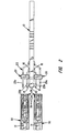
- the present invention includes a printed circuit board 10 having at least one signal trace (not shown) and at least one ground trace (not shown).
- the signal trace is connected to a signal contact pad 16, while the ground trace is connected to a ground contact pad 18.
- a pin header 20 includes a plurality of contact pins 22 extending from a first pin end 22a attached to circuit board 10 to a second pin end 22b.
- pin header 20 is shown and described herein as a surface mount pin header, pin header 20 may also be a through-hole pin header or any other suitable type of pin header known in the art. Pin headers are commonly available from a variety of sources, including, for example, Samtec of New Albany, IN, AMP of Harrisburg, PA, and Minnesota Mining and Manufacturing Company of St. Paul, MN.
- the commonly available pin headers 20 include two rows 23a, 23b of contact pins 22. Typically, one row of pins is connected to a ground plane, while the second row of pins is connected to the circuit board signal traces. Most commonly, first row 23a (the row that is farthest from the printed circuit board 10) is connected to a ground plane, while second row 23b (the row that is closes to the printed circuit board 10) is connected to the signal traces of the printed circuit board 10. Of course, various combinations of pins 22 in rows 23a and 23b may be electrically connected to circuit board 10 in any number of ways.
- first row 23a of pins 22 is secured to the printed circuit board 10 only to lend additional mechanical stability to the pin header 20. That is, the pins 22 in row 23a are not electrically connected to any elements on printed circuit board 10 and could be eliminated. Alternately, pins 22 of row 23a may remain in electrical contact with the ground plane of circuit board 10. It should be noted that first row 23a is the row with the longest unshielded path through the interconnection, and for that reason the pins 22 of first row 23b are preferably used for electrical connection to the signal traces on printed circuit board 10. It will also be recognized that a pin header having only a single row of pins (for connection to signal contact pads 16) could be used, with the pin header being stabilized on circuit board 10 by means other than a second row of pins 22 as is illustrated in the Figures.
- circuit board 10 may include a pin header 20 on both sides of the circuit board 10, with similarly positioned signal pads 16 and ground contact pads 18.
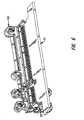
- the inventive assembly also includes a connector carrier 30 for receiving the second ends 22b of the contact pins 22 and connecting them to coaxial cable 31.
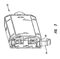
- the connector carrier 30 includes a plurality of coaxial cable terminations 32 positioned within the connector housing 34. An enlarged view of a single coaxial cable termination 32 is shown in Figure 3. Each of the plurality of coaxial cable terminations 32 is adapted to receive second ends 22b of a mating signal contact pins 22.
- each coaxial cable termination 32 includes a contact beam 36 adjacent its leading edge 38 for making electrical contact with the ground contact pad 18 on the printed circuit board 10 as the connector carrier 30 engages the pin header 20.
- the electrical path from the printed circuit board 10 to the coaxial cable 31 is made as short as possible, thereby dramatically improving the performance of the connector carrier 30 over what would be otherwise expected with a surface mount pin header 20.
- a connector carrier 30 is provided for each pin header 20 on printed circuit board 10, with one connector positioned on either side of the printed circuit board 10.
- the use of connector carrier 30 on either side of printed circuit board 10 is preferred to balance the mechanical contacting force between the printed circuit board 10 and the coaxial cable terminations 32, thereby preventing the printed circuit board 10 from bending or warping over time.
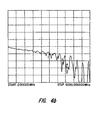
- Figures 4a-4c plot the attenuation or loss of a sine wave signal traveling through an interconnection system over a range of frequencies.
- the test method for creating this data is well known in the art. The data was generated using a Tektronix CSA 803 Communications Signal Analyzer with an SD-24 TDR Sampling Head.
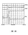
- Figure 4a illustrates the interconnect performance when the ground path is routed through a contact pin 22 of row 23a in the conventional manner. It is generally accepted that an attenuation of greater than -3dB (equating approximately to V out /V in of 0.707) is not acceptable. It can be easily seen from Figure 4a that the conventional type of interconnection system provides satisfactory performance only up to about 800 megahertz. This low interconnection system bandwidth is clearly not acceptable for current high performance systems.
- Figure 4b illustrates the improved performance of the interconnect system when the ground path is routed only through contact beam 36 to contact pad 18 at edge 42 of printed circuit board 10. It can be seen that routing the ground path through contact beam 36 and ground contact pad 18 immediately adjacent edge 42 of printed circuit board 10 provides an improved system performance.
- the inventive interconnection system described herein provides satisfactory performance up to about 4.3 gigahertz. This is clearly a dramatic and unexpected improvement over the conventional interconnection system of Figure 4a.
- Figure 4c illustrates the improved performance of the interconnect system when the ground path is routed both through contact beam 36 to contact pad 18 and through contact pin 22 of first row 23a.
- the combination of grounding through both contact beam 36 and contact pin 22 of row 23 provides even better performance than using contact beam 36 alone. As shown in Figure 4c, this combination yields satisfactory performance up to about 4.8 gigahertz.
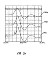
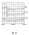
- FIGS 5a-5c show Time Domain Reflectometer (TDR) plots for the connectors of Figures 4a-4e.
- the TDR plots illustrate the changes in impedance as a signal travels through the interconnection system, with rise times of 250 picoseconds, 100 picoseconds, and 35 picoseconds.
- a TDR plot of a system will have a constant impedance.
- one goal is to minimize the changes in impedance as the signal travels through the interconnection system. By minimizing the changes in impedance, distortion and attenuation of the signal are reduced, thereby improving the system performance.
- a separate power connector 50 may be mated to signal connector carrier 30 as is shown in Figure 1.
- Power connector 50 connects to pin header 52 in a manner known in the art.
- the connectors 30, 50 placed on opposite sides of printed circuit board 10 include guides 60 with lead-in features 62 to properly position connectors 30, 50 on printed circuit board 10.
- Connectors 30, 50 are shown mated .to pin headers 20 on circuit board 10 in Figure 6.
- Connectors 30, 50 are preferably resiliently secured against each other, such as by an elastic band or other means (not shown) which urges the connectors toward each other and against printed circuit board 10. In this manner, the connectors 30, 50 are allowed to independently "float” on circuit board 10. The ability to float on circuit board 10 permits accommodation of variations in circuit board thickness which are normal in the industry.
- Connectors 30, 50 also include mounting tabs or ears 64 for receiving screws 66 for securing connectors 30, 50 to the electronic device (not shown) holding printed circuit board 10.
Landscapes
- Coupling Device And Connection With Printed Circuit (AREA)
- Details Of Connecting Devices For Male And Female Coupling (AREA)
- Multi-Conductor Connections (AREA)
Claims (11)
- Elektrische Verbinderbaugruppe zum Übertragen elektrischer Hochgeschwindigkeitssignale, wobei die Baugruppe aufweist:dadurch gekennzeichnet, dass sie ferner aufweist:eine Leiterplatte (10), die mindestens eine Signalleiterbahn und mindestens eine Erdungsleiterbahn aufweist, wobei die Signalleiterbahn mit einer Signalkontaktanschlussfläche (16) verbunden ist und die Erdungsleiterbahn mit einer Erdungskontaktanschlussfläche (18) verbunden ist,einen ersten Pin-Header (20), der mindestens einen Kontaktstift (22) aufweist, wobei ein erstes Ende des Kontaktstiftes mit der Signalkontaktanschlussfläche verbunden ist, undeinen ersten Verbinder (30) zum Aufnehmen eines zweiten Endes des mindestens einen Kontaktstiftes, wobei der Verbinder einen Kontaktstreifen zum direkten Kontaktieren der Erdungskontaktanschlussfläche aufweist.
- Elektrische Verbinderbaugruppe nach Anspruch 1, wobei die Erdungskontaktanschlussfläche einem Rand der Leiterplatte benachbart positioniert ist.
- Elektrische Verbinderbaugruppe nach Anspruch 1 oder 2, wobei der erste Verbinder Abschlüsse für Koaxialkabel aufweist, wobei die Abschlüsse derart ausgebildet sind, dass sie das zweite Ende des Kontaktstiftes aufzunehmen und den Kontaktstreifen halten.
- Elektrische Verbinderbaugruppe nach einem der Ansprüche 1 bis 3, wobei die Baugruppe einen Signalverlust von weniger als -3 dB bei Frequenzen größer als 1 Gigahertz aufweist.
- Elektrische Verbinderbaugruppe nach einem der Ansprüche 1 bis 4, wobei die Baugruppe einen Signalverlust von weniger als -3 dB bei Frequenzen innerhalb des Bereiches von 1 bis 5 Gigahertz aufweist.
- Elektrische Verbinderbaugruppe nach einem der Ansprüche 1 bis 5, wobei die Baugruppe eine Variation in der Impedanz von weniger als 10 Ohm bei einem Signal aufweist, das eine Anstiegszeit von 250 Picosekunden aufweist.
- Elektrische Verbinderbaugruppe nach einem der Ansprüche 1 bis 6, wobei die Leiterplatte mindestens eine Signalkontaktanschlussfläche und mindestens eine Erdungskontaktanschlussfläche auf jeder Seite der Leiterplatte aufweist, ferner mit einem zweiten Pin-Header und einen zweiten Verbinder auf jeder Seite der Leiterplatte aufweist.
- Elektrische Verbinderbaugruppe nach Anspruch 7, wobei die ersten und zweiten Verbinder unabhängig auf der Leiterplatte auf freiem Potential liegen.
- Elektrische Verbinderbaugruppe nach Anspruch 7 oder 8, wobei die ersten und zweiten Verbinder federnd aneinander gesichert sind.
- Elektrische Verbinderbaugruppe nach einem der Ansprüche 1 bis 9, wobei der Pin-Header ein Pin-Header für Oberflächenmontage ist.
- Elektrische Verbinderbaugruppe nach einem der Ansprüche 1 bis 9, wobei der Pin-Header ein Pin-Header für Durchkontaktierung ist.
Priority Applications (1)
| Application Number | Priority Date | Filing Date | Title |
|---|---|---|---|
| EP05101450A EP1553664B1 (de) | 2000-05-05 | 2000-11-09 | Hochgeschwindigkeitsstecker und Verbindung für Leiterplatte |
Applications Claiming Priority (3)
| Application Number | Priority Date | Filing Date | Title |
|---|---|---|---|
| US09/565,707 US6368120B1 (en) | 2000-05-05 | 2000-05-05 | High speed connector and circuit board interconnect |
| US565707 | 2000-05-05 | ||
| PCT/US2000/031137 WO2001086757A1 (en) | 2000-05-05 | 2000-11-09 | High speed connector and circuit board interconnect |
Related Child Applications (1)
| Application Number | Title | Priority Date | Filing Date |
|---|---|---|---|
| EP05101450A Division EP1553664B1 (de) | 2000-05-05 | 2000-11-09 | Hochgeschwindigkeitsstecker und Verbindung für Leiterplatte |
Publications (2)
| Publication Number | Publication Date |
|---|---|
| EP1279207A1 EP1279207A1 (de) | 2003-01-29 |
| EP1279207B1 true EP1279207B1 (de) | 2005-03-30 |
Family
ID=24259772
Family Applications (2)
| Application Number | Title | Priority Date | Filing Date |
|---|---|---|---|
| EP00978580A Expired - Lifetime EP1279207B1 (de) | 2000-05-05 | 2000-11-09 | Hochgeschwindigkeitsstecker und verbindung für leiterplatte |
| EP05101450A Expired - Lifetime EP1553664B1 (de) | 2000-05-05 | 2000-11-09 | Hochgeschwindigkeitsstecker und Verbindung für Leiterplatte |
Family Applications After (1)
| Application Number | Title | Priority Date | Filing Date |
|---|---|---|---|
| EP05101450A Expired - Lifetime EP1553664B1 (de) | 2000-05-05 | 2000-11-09 | Hochgeschwindigkeitsstecker und Verbindung für Leiterplatte |
Country Status (7)
| Country | Link |
|---|---|
| US (1) | US6368120B1 (de) |
| EP (2) | EP1279207B1 (de) |
| JP (1) | JP4825390B2 (de) |
| AT (1) | ATE292330T1 (de) |
| AU (1) | AU2001216032A1 (de) |
| DE (2) | DE60032954T2 (de) |
| WO (1) | WO2001086757A1 (de) |
Families Citing this family (32)
| Publication number | Priority date | Publication date | Assignee | Title |
|---|---|---|---|---|
| US6780069B2 (en) * | 2002-12-12 | 2004-08-24 | 3M Innovative Properties Company | Connector assembly |
| DE102004043763B3 (de) * | 2004-09-10 | 2006-02-02 | Adc Gmbh | Verteilermodul zur Umsetzung zwischen symmetrischen und unsymmetrischen Datenübertragungsstrecken |
| US7090501B1 (en) | 2005-03-22 | 2006-08-15 | 3M Innovative Properties Company | Connector apparatus |
| US20070141871A1 (en) * | 2005-12-19 | 2007-06-21 | 3M Innovative Properties Company | Boardmount header to cable connector assembly |
| US7731528B2 (en) * | 2006-01-31 | 2010-06-08 | 3M Innovative Properties Company | Electrical termination device |
| US7553187B2 (en) * | 2006-01-31 | 2009-06-30 | 3M Innovative Properties Company | Electrical connector assembly |
| US7651355B2 (en) * | 2006-06-30 | 2010-01-26 | 3M Innovative Properties Company | Floating panel mount connection system |
| US7744403B2 (en) * | 2006-11-29 | 2010-06-29 | 3M Innovative Properties Company | Connector for electrical cables |
| US7445471B1 (en) | 2007-07-13 | 2008-11-04 | 3M Innovative Properties Company | Electrical connector assembly with carrier |
| US8007308B2 (en) * | 2007-10-17 | 2011-08-30 | 3M Innovative Properties Company | Electrical connector assembly |
| CN101828308B (zh) * | 2007-10-19 | 2013-06-12 | 3M创新有限公司 | 电连接器组件 |
| US7722394B2 (en) | 2008-02-21 | 2010-05-25 | 3M Innovative Properties Company | Electrical termination device |
| US7651374B2 (en) * | 2008-06-10 | 2010-01-26 | 3M Innovative Properties Company | System and method of surface mount electrical connection |
| US7744414B2 (en) * | 2008-07-08 | 2010-06-29 | 3M Innovative Properties Company | Carrier assembly and system configured to commonly ground a header |
| US7892007B2 (en) | 2008-08-15 | 2011-02-22 | 3M Innovative Properties Company | Electrical connector assembly |
| US7789676B2 (en) * | 2008-08-19 | 2010-09-07 | Tyco Electronics Corporation | Electrical connector with electrically shielded terminals |
| US20100068944A1 (en) * | 2008-09-18 | 2010-03-18 | 3M Innovative Properties Company | Electrical connector and circuit board interconnect |
| US9011177B2 (en) | 2009-01-30 | 2015-04-21 | Molex Incorporated | High speed bypass cable assembly |
| US7850489B1 (en) | 2009-08-10 | 2010-12-14 | 3M Innovative Properties Company | Electrical connector system |
| US7909646B2 (en) * | 2009-08-10 | 2011-03-22 | 3M Innovative Properties Company | Electrical carrier assembly and system of electrical carrier assemblies |
| US7997933B2 (en) * | 2009-08-10 | 2011-08-16 | 3M Innovative Properties Company | Electrical connector system |
| US7927144B2 (en) * | 2009-08-10 | 2011-04-19 | 3M Innovative Properties Company | Electrical connector with interlocking plates |
| CN102823073A (zh) | 2010-02-01 | 2012-12-12 | 3M创新有限公司 | 电连接器和组件 |
| US9136652B2 (en) * | 2012-02-07 | 2015-09-15 | Fci Americas Technology Llc | Electrical connector assembly |
| US9142921B2 (en) | 2013-02-27 | 2015-09-22 | Molex Incorporated | High speed bypass cable for use with backplanes |
| EP3042420A4 (de) | 2013-09-04 | 2017-04-05 | Molex, LLC | Steckverbindersystem mit kabelbypass |
| KR102299742B1 (ko) | 2015-01-11 | 2021-09-09 | 몰렉스 엘엘씨 | 회로 기판 바이패스 조립체 및 그를 위한 구성요소 |
| KR20170102011A (ko) | 2015-01-11 | 2017-09-06 | 몰렉스 엘엘씨 | 바이패스 루트설정 조립체에 사용하기 적합한 와이어-대-기판 커넥터 |
| WO2016179263A1 (en) | 2015-05-04 | 2016-11-10 | Molex, Llc | Computing device using bypass assembly |
| US10424878B2 (en) | 2016-01-11 | 2019-09-24 | Molex, Llc | Cable connector assembly |
| KR102092627B1 (ko) | 2016-01-11 | 2020-03-24 | 몰렉스 엘엘씨 | 루트설정 조립체 및 이를 사용한 시스템 |
| US11151300B2 (en) | 2016-01-19 | 2021-10-19 | Molex, Llc | Integrated routing assembly and system using same |
Family Cites Families (11)
| Publication number | Priority date | Publication date | Assignee | Title |
|---|---|---|---|---|
| JPS4934430B1 (de) * | 1969-12-26 | 1974-09-13 | ||
| US4628410A (en) | 1985-04-10 | 1986-12-09 | Itt Corporation | Surface mounting connector |
| US4690479A (en) * | 1985-10-10 | 1987-09-01 | Amp Incorporated | Filtered electrical header assembly |
| US4659155A (en) * | 1985-11-19 | 1987-04-21 | Teradyne, Inc. | Backplane-daughter board connector |
| US4795352A (en) * | 1988-02-01 | 1989-01-03 | Amp Incorporated | Microcoaxial connector family |
| DE9016083U1 (de) | 1990-11-27 | 1991-02-14 | Thomas & Betts Corp., Bridgewater, N.J. | Stecker |
| JP3294634B2 (ja) * | 1991-04-26 | 2002-06-24 | アンプ インコーポレイテッド | 電気コネクタ |
| FR2747516B1 (fr) | 1996-04-12 | 1998-06-05 | Framatome Connectors France | Connecteur blinde, notamment du type comprenant une fiche et une embase destinee a etre fixee a un support plan |
| US5944536A (en) * | 1996-10-31 | 1999-08-31 | Thomas & Betts Corporation | Cover for an edge mounted printed circuit board connector |
| US6024587A (en) | 1997-06-26 | 2000-02-15 | Garth; Emory C. | High speed circuit interconnection apparatus |
| JP2000171724A (ja) * | 1998-12-04 | 2000-06-23 | Olympus Optical Co Ltd | 電気的コネクタ |
-
2000
- 2000-05-05 US US09/565,707 patent/US6368120B1/en not_active Expired - Lifetime
- 2000-11-09 WO PCT/US2000/031137 patent/WO2001086757A1/en active IP Right Grant
- 2000-11-09 EP EP00978580A patent/EP1279207B1/de not_active Expired - Lifetime
- 2000-11-09 JP JP2001582871A patent/JP4825390B2/ja not_active Expired - Fee Related
- 2000-11-09 EP EP05101450A patent/EP1553664B1/de not_active Expired - Lifetime
- 2000-11-09 AT AT00978580T patent/ATE292330T1/de not_active IP Right Cessation
- 2000-11-09 AU AU2001216032A patent/AU2001216032A1/en not_active Abandoned
- 2000-11-09 DE DE60032954T patent/DE60032954T2/de not_active Expired - Lifetime
- 2000-11-09 DE DE60019170T patent/DE60019170T2/de not_active Expired - Lifetime
Also Published As
| Publication number | Publication date |
|---|---|
| DE60032954T2 (de) | 2007-10-25 |
| DE60032954D1 (de) | 2007-02-22 |
| EP1553664B1 (de) | 2007-01-10 |
| ATE292330T1 (de) | 2005-04-15 |
| JP2003533845A (ja) | 2003-11-11 |
| AU2001216032A1 (en) | 2001-11-20 |
| EP1553664A1 (de) | 2005-07-13 |
| US6368120B1 (en) | 2002-04-09 |
| DE60019170D1 (de) | 2005-05-04 |
| DE60019170T2 (de) | 2006-01-26 |
| WO2001086757A1 (en) | 2001-11-15 |
| JP4825390B2 (ja) | 2011-11-30 |
| EP1279207A1 (de) | 2003-01-29 |
Similar Documents
| Publication | Publication Date | Title |
|---|---|---|
| EP1279207B1 (de) | Hochgeschwindigkeitsstecker und verbindung für leiterplatte | |
| JP6676019B2 (ja) | ケーブルバイパスを備えるコネクタシステム | |
| US20230253737A1 (en) | Electrical connector system | |
| US7651374B2 (en) | System and method of surface mount electrical connection | |
| US6776659B1 (en) | High speed, high density electrical connector | |
| US6814619B1 (en) | High speed, high density electrical connector and connector assembly | |
| CN112930628B (zh) | 用于高频信号的混合电连接器 | |
| US7508681B2 (en) | Printed circuit board for high speed, high density electrical connector with improved cross-talk minimization attenuation and impedance mismatch characteristics | |
| US20090215309A1 (en) | Direct attach electrical connector | |
| US6780059B1 (en) | High speed, high density electrical connector | |
| EP2212971A2 (de) | Elektrische verbinderbaugruppe | |
| US7285025B2 (en) | Enhanced jack with plug engaging printed circuit board | |
| US5823795A (en) | Connector between a daughterboard and a motherboard for high-speed single-ended electrical signals | |
| US6695646B1 (en) | Electrical connector having floatable chicklets | |
| JPS6367845A (ja) | 一定の電気特性を有するバス構造 | |
| US11495898B2 (en) | Connector paddle card with improved wiring connection geometry | |
| US20230299520A1 (en) | Interconnection system, case assembly, electrical connector, assembly and connector assembly using detachable, cabled front-panel connector | |
| US6283795B1 (en) | Electrical connector with reduced attenuation, near-end cross talk, and return loss | |
| KR100541246B1 (ko) | 차동 쌍 접속 장치 | |
| WO2003092121A2 (en) | Three dimensional, high speed back-panel interconnection system |
Legal Events
| Date | Code | Title | Description |
|---|---|---|---|
| PUAI | Public reference made under article 153(3) epc to a published international application that has entered the european phase |
Free format text: ORIGINAL CODE: 0009012 |
|
| 17P | Request for examination filed |
Effective date: 20021105 |
|
| AK | Designated contracting states |
Designated state(s): AT BE CH CY DE DK ES FI FR GB GR IE IT LI LU MC NL PT SE |
|
| AX | Request for extension of the european patent |
Extension state: AL LT LV MK RO SI |
|
| GRAP | Despatch of communication of intention to grant a patent |
Free format text: ORIGINAL CODE: EPIDOSNIGR1 |
|
| RIC1 | Information provided on ipc code assigned before grant |
Ipc: 7H 01R 12/20 B Ipc: 7H 01R 23/70 B Ipc: 7H 01R 12/16 A |
|
| RIC1 | Information provided on ipc code assigned before grant |
Ipc: 7H 01R 12/16 A Ipc: 7H 01R 12/20 B Ipc: 7H 01R 23/70 B |
|
| RBV | Designated contracting states (corrected) |
Designated state(s): AT BE CH CY DE DK ES FI FR GB GR IE IT LI LU MC NL PT SE TR |
|
| GRAS | Grant fee paid |
Free format text: ORIGINAL CODE: EPIDOSNIGR3 |
|
| GRAA | (expected) grant |
Free format text: ORIGINAL CODE: 0009210 |
|
| AK | Designated contracting states |
Kind code of ref document: B1 Designated state(s): AT BE CH CY DE DK ES FI FR GB GR IE IT LI LU MC NL PT SE TR |
|
| PG25 | Lapsed in a contracting state [announced via postgrant information from national office to epo] |
Ref country code: IT Free format text: LAPSE BECAUSE OF FAILURE TO SUBMIT A TRANSLATION OF THE DESCRIPTION OR TO PAY THE FEE WITHIN THE PRESCRIBED TIME-LIMIT;WARNING: LAPSES OF ITALIAN PATENTS WITH EFFECTIVE DATE BEFORE 2007 MAY HAVE OCCURRED AT ANY TIME BEFORE 2007. THE CORRECT EFFECTIVE DATE MAY BE DIFFERENT FROM THE ONE RECORDED. Effective date: 20050330 Ref country code: LI Free format text: LAPSE BECAUSE OF FAILURE TO SUBMIT A TRANSLATION OF THE DESCRIPTION OR TO PAY THE FEE WITHIN THE PRESCRIBED TIME-LIMIT Effective date: 20050330 Ref country code: FI Free format text: LAPSE BECAUSE OF FAILURE TO SUBMIT A TRANSLATION OF THE DESCRIPTION OR TO PAY THE FEE WITHIN THE PRESCRIBED TIME-LIMIT Effective date: 20050330 Ref country code: TR Free format text: LAPSE BECAUSE OF FAILURE TO SUBMIT A TRANSLATION OF THE DESCRIPTION OR TO PAY THE FEE WITHIN THE PRESCRIBED TIME-LIMIT Effective date: 20050330 Ref country code: CH Free format text: LAPSE BECAUSE OF FAILURE TO SUBMIT A TRANSLATION OF THE DESCRIPTION OR TO PAY THE FEE WITHIN THE PRESCRIBED TIME-LIMIT Effective date: 20050330 Ref country code: BE Free format text: LAPSE BECAUSE OF FAILURE TO SUBMIT A TRANSLATION OF THE DESCRIPTION OR TO PAY THE FEE WITHIN THE PRESCRIBED TIME-LIMIT Effective date: 20050330 Ref country code: AT Free format text: LAPSE BECAUSE OF FAILURE TO SUBMIT A TRANSLATION OF THE DESCRIPTION OR TO PAY THE FEE WITHIN THE PRESCRIBED TIME-LIMIT Effective date: 20050330 Ref country code: NL Free format text: LAPSE BECAUSE OF FAILURE TO SUBMIT A TRANSLATION OF THE DESCRIPTION OR TO PAY THE FEE WITHIN THE PRESCRIBED TIME-LIMIT Effective date: 20050330 |
|
| REG | Reference to a national code |
Ref country code: GB Ref legal event code: FG4D |
|
| RIC1 | Information provided on ipc code assigned before grant |
Ipc: 7H 01R 12/16 A Ipc: 7H 01R 12/20 B |
|
| REG | Reference to a national code |
Ref country code: CH Ref legal event code: EP |
|
| REF | Corresponds to: |
Ref document number: 60019170 Country of ref document: DE Date of ref document: 20050504 Kind code of ref document: P |
|
| REG | Reference to a national code |
Ref country code: IE Ref legal event code: FG4D |
|
| PG25 | Lapsed in a contracting state [announced via postgrant information from national office to epo] |
Ref country code: DK Free format text: LAPSE BECAUSE OF FAILURE TO SUBMIT A TRANSLATION OF THE DESCRIPTION OR TO PAY THE FEE WITHIN THE PRESCRIBED TIME-LIMIT Effective date: 20050630 Ref country code: GR Free format text: LAPSE BECAUSE OF FAILURE TO SUBMIT A TRANSLATION OF THE DESCRIPTION OR TO PAY THE FEE WITHIN THE PRESCRIBED TIME-LIMIT Effective date: 20050630 |
|
| PG25 | Lapsed in a contracting state [announced via postgrant information from national office to epo] |
Ref country code: ES Free format text: LAPSE BECAUSE OF FAILURE TO SUBMIT A TRANSLATION OF THE DESCRIPTION OR TO PAY THE FEE WITHIN THE PRESCRIBED TIME-LIMIT Effective date: 20050711 |
|
| PG25 | Lapsed in a contracting state [announced via postgrant information from national office to epo] |
Ref country code: PT Free format text: LAPSE BECAUSE OF FAILURE TO SUBMIT A TRANSLATION OF THE DESCRIPTION OR TO PAY THE FEE WITHIN THE PRESCRIBED TIME-LIMIT Effective date: 20050908 |
|
| REG | Reference to a national code |
Ref country code: CH Ref legal event code: PL |
|
| NLV1 | Nl: lapsed or annulled due to failure to fulfill the requirements of art. 29p and 29m of the patents act | ||
| PG25 | Lapsed in a contracting state [announced via postgrant information from national office to epo] |
Ref country code: IE Free format text: LAPSE BECAUSE OF NON-PAYMENT OF DUE FEES Effective date: 20051109 Ref country code: GB Free format text: LAPSE BECAUSE OF NON-PAYMENT OF DUE FEES Effective date: 20051109 Ref country code: CY Free format text: LAPSE BECAUSE OF FAILURE TO SUBMIT A TRANSLATION OF THE DESCRIPTION OR TO PAY THE FEE WITHIN THE PRESCRIBED TIME-LIMIT Effective date: 20051109 |
|
| PG25 | Lapsed in a contracting state [announced via postgrant information from national office to epo] |
Ref country code: MC Free format text: LAPSE BECAUSE OF NON-PAYMENT OF DUE FEES Effective date: 20051130 Ref country code: LU Free format text: LAPSE BECAUSE OF NON-PAYMENT OF DUE FEES Effective date: 20051130 |
|
| PLBE | No opposition filed within time limit |
Free format text: ORIGINAL CODE: 0009261 |
|
| STAA | Information on the status of an ep patent application or granted ep patent |
Free format text: STATUS: NO OPPOSITION FILED WITHIN TIME LIMIT |
|
| ET | Fr: translation filed | ||
| 26N | No opposition filed |
Effective date: 20060102 |
|
| GBPC | Gb: european patent ceased through non-payment of renewal fee |
Effective date: 20051109 |
|
| REG | Reference to a national code |
Ref country code: IE Ref legal event code: MM4A |
|
| PG25 | Lapsed in a contracting state [announced via postgrant information from national office to epo] |
Ref country code: SE Free format text: LAPSE BECAUSE OF FAILURE TO SUBMIT A TRANSLATION OF THE DESCRIPTION OR TO PAY THE FEE WITHIN THE PRESCRIBED TIME-LIMIT Effective date: 20050630 |
|
| PGFP | Annual fee paid to national office [announced via postgrant information from national office to epo] |
Ref country code: DE Payment date: 20101104 Year of fee payment: 11 |
|
| PGFP | Annual fee paid to national office [announced via postgrant information from national office to epo] |
Ref country code: FR Payment date: 20111118 Year of fee payment: 12 |
|
| REG | Reference to a national code |
Ref country code: FR Ref legal event code: ST Effective date: 20130731 |
|
| REG | Reference to a national code |
Ref country code: DE Ref legal event code: R119 Ref document number: 60019170 Country of ref document: DE Effective date: 20130601 |
|
| PG25 | Lapsed in a contracting state [announced via postgrant information from national office to epo] |
Ref country code: DE Free format text: LAPSE BECAUSE OF NON-PAYMENT OF DUE FEES Effective date: 20130601 |
|
| PG25 | Lapsed in a contracting state [announced via postgrant information from national office to epo] |
Ref country code: FR Free format text: LAPSE BECAUSE OF NON-PAYMENT OF DUE FEES Effective date: 20121130 |