EP1278204A2 - Semiconductor integrated circuit - Google Patents
Semiconductor integrated circuit Download PDFInfo
- Publication number
- EP1278204A2 EP1278204A2 EP02254341A EP02254341A EP1278204A2 EP 1278204 A2 EP1278204 A2 EP 1278204A2 EP 02254341 A EP02254341 A EP 02254341A EP 02254341 A EP02254341 A EP 02254341A EP 1278204 A2 EP1278204 A2 EP 1278204A2
- Authority
- EP
- European Patent Office
- Prior art keywords
- circuit blocks
- circuit
- cam
- circuits
- memory cell
- Prior art date
- Legal status (The legal status is an assumption and is not a legal conclusion. Google has not performed a legal analysis and makes no representation as to the accuracy of the status listed.)
- Granted
Links
Images


Classifications
-
- G—PHYSICS
- G11—INFORMATION STORAGE
- G11C—STATIC STORES
- G11C29/00—Checking stores for correct operation ; Subsequent repair; Testing stores during standby or offline operation
-
- G—PHYSICS
- G11—INFORMATION STORAGE
- G11C—STATIC STORES
- G11C29/00—Checking stores for correct operation ; Subsequent repair; Testing stores during standby or offline operation
- G11C29/70—Masking faults in memories by using spares or by reconfiguring
- G11C29/78—Masking faults in memories by using spares or by reconfiguring using programmable devices
- G11C29/80—Masking faults in memories by using spares or by reconfiguring using programmable devices with improved layout
-
- G—PHYSICS
- G11—INFORMATION STORAGE
- G11C—STATIC STORES
- G11C15/00—Digital stores in which information comprising one or more characteristic parts is written into the store and in which information is read-out by searching for one or more of these characteristic parts, i.e. associative or content-addressed stores
-
- G—PHYSICS
- G11—INFORMATION STORAGE
- G11C—STATIC STORES
- G11C15/00—Digital stores in which information comprising one or more characteristic parts is written into the store and in which information is read-out by searching for one or more of these characteristic parts, i.e. associative or content-addressed stores
- G11C15/04—Digital stores in which information comprising one or more characteristic parts is written into the store and in which information is read-out by searching for one or more of these characteristic parts, i.e. associative or content-addressed stores using semiconductor elements
- G11C15/046—Digital stores in which information comprising one or more characteristic parts is written into the store and in which information is read-out by searching for one or more of these characteristic parts, i.e. associative or content-addressed stores using semiconductor elements using non-volatile storage elements
-
- H—ELECTRICITY
- H10—SEMICONDUCTOR DEVICES; ELECTRIC SOLID-STATE DEVICES NOT OTHERWISE PROVIDED FOR
- H10D—INORGANIC ELECTRIC SEMICONDUCTOR DEVICES
- H10D89/00—Aspects of integrated devices not covered by groups H10D84/00 - H10D88/00
- H10D89/10—Integrated device layouts
Definitions
- the present invention relates to a semiconductor integrated circuit, and more particularly to a semiconductor integrated circuit used as a semiconductor memory device or the like having a redundancy relief function for substituting a normal memory cell for a malfunctioning memory cell.
- a conventionally-known semiconductor integrated circuit includes a plurality of adjacent output circuit blocks having the same circuit layouts, i.e., shapes and areas of the output circuit blocks, positions of signal terminals thereof, etc., are the same, and a plurality of adjacent input circuit blocks having the same circuit layouts.
- an output signal provided from each output circuit block is input to a corresponding one of the input circuit blocks.
- the input and output circuit blocks can be connected using straight conductor lines such that a distance between the input circuit blocks and their corresponding output circuit blocks is the shortest possible, and therefore there are no unnecessary areas in the circuit layout.
- the pitch between the adjacent output circuit blocks is not identical to the pitch between the adjacent input circuit blocks, the conductor lines for connecting the input and output circuit blocks are required to be bent so as not cross one another avoiding a short circuit, thereby increasing an area of a conductor region in which the conductor lines are provided.
- the flash memory which is a nonvolatile semiconductor memory.
- the flash memory includes spare flash memory cells.
- the spare flash memory cell When there is a malfunction in a main memory cell, the spare flash memory cell is substituted for the malfunctioning main memory cell (malfunctioning memory cell) such that data read/write operations or the like can be performed on the spare flash memory cell.
- the flash memory usually uses a redundant circuit so as to substitute the spare flash memory cell for the malfunctioning memory cell.
- the redundant circuit includes a memory circuit for storing address information of the malfunctioning memory cell when the malfunctioning memory cell is present and a redundancy relief comparison circuit for comparing the address information of the malfunctioning memory cell and address information externally input to the redundant circuit.
- a plurality of fuses made of polysilicon, metal or the like are provided in order to store the address information of the malfunctioning memory cell.
- the plurality of fuses are electrically disconnected, for example.
- the flash memory which is a nonvolatile semiconductor memory for example, memory cells, which are nonvolatile semiconductor memory elements, are used instead of using fuses so as to store address information of a malfunctioning memory cell on which redundancy relief is performed and other information specific to the flash memory.
- the memory circuit using the memory cells which are the nonvolatile semiconductor memory elements is referred to as a CAM (contents addressable memory) circuit.
- a CAM circuit usually includes two floating gate-type transistors 2 and 3 , four N-type transistors 4 , 5 , 6 and 7 , and two P-type transistors 8 and 9 .
- the P-type transistor 8, the N-type transistor 4 and the floating gate-type transistor 2 are serially connected together in this order.
- a power supply voltage VCC is applied to a source of the P-type transistor 8.
- the floating gate-type transistor 2 is connected to a drain of the P-type transistor 8 via the N-type transistor 4.
- a ground potential Vss is applied to a source of the floating gate-type transistor 2.
- the P-type transistor 9 , the N-type transistor 5 and the floating gate-type transistor 3 are serially connected together in this order.
- the power supply voltage VCC is applied to a source of the P-type transistor 9.
- the floating gate-type transistor 3 is connected to a drain of the P-type transistor 9 via the N-type transistor 5.
- the ground potential Vss is applied to a source of the floating gate-type transistor 3.
- An output Vgate is provided by a bias voltage generation circuit 10 to a gate of each of the floating gate-type transistors 2 and 3 .
- An output VB is provided by a bias voltage generation circuit 11 to a gate of each of the N-type transistors 4 and 5.
- a gate of the P-type transistor 8 is connected to a node N4 to which the P-type transistor 9 and the N-type transistor 5 are connected.
- a gate of the P-type transistor 9 is connected to a node N3 to which the P-type transistor 8 and the N-type transistor 4 are connected.
- a program voltage Vprg is applied by a voltage supply circuit (not shown) to a drain of each of the N-type transistors 6 and 7.
- Program signals PRG1 and PRG2 are applied by their respective control circuits (not shown) to gates of the N-type transistors 6 and 7 , respectively.
- a source of the N-type transistor 6 is connected to a node N1 to which the floating gate-type transistor 2 and the N-type transistor 4 are connected.
- a source of the N-type transistor 7 is connected to a node N2 to which the floating gate-type transistor 3 and the N-type transistor 5 are connected.
- the CAM circuit configured as described above can store only one bit of address information of the malfunctioning memory cell on which redundancy relief is performed.
- a plurality of CAM circuits together store the entire address information of the malfunctioning memory cell.
- an output terminal OUT1 of the CAM circuit is connected to a redundancy relief address comparison circuit (not shown).
- Outputs from the plurality of CAM circuits which together store the address information of the malfunctioning memory cell are compared to an externally-input address by the redundancy relief comparison circuit.
- the comparison results in a mismatch access to a memory cell corresponding to the externally-input address is performed.
- access to the spare memory cell is performed.
- the CAM circuit includes two flash memory cells each being similar to the main memory cell, a circuit layout with respect to a position in which the CAM circuit is provided, a pitch between the CAM circuits, etc., is considerably restricted by a layout of the main memory cells.
- Figure 3 is a diagram for explaining that the position of the CAM circuit is restricted by the layout of the main memory cells.
- the flash memory includes in a main memory region 21 a plurality of floating gate-type transistors 20 which are the flash memories constituting the main memory and are provided in a matrix form.
- Each control gate of the plurality of floating gate-type transistors (flash memory cells) 20 provided in one direction is connected to word lines 22 or 26 (i.e., the word lines 22 are provided in odd columns and word lines 26 are provided in even columns).
- the word lines 22 and 26 are connected to a word line voltage control circuit 23.
- the word line voltage control circuit 23 controls an operation so as to write/read/erase data in/from/from the flash memory cell 20
- the externally-input address information is decoded so as to select one of the word lines 22 or 26 corresponding to the decoded address information, and then a voltage having a prescribed value is applied to the selected word lines 22 or 26 .
- the CAM circuit is positioned in regions 24 or 25 which are provided so as to adjacent to the main memory region 21 along a direction perpendicular to the word lines 22 and 26 .
- the position of the CAM circuit is restricted by the layout of the main memory cells, by providing the CAM circuit and the main memory cell region 21 so as to be adjacent to each other, a decoder element which constitutes the word line voltage control circuit 23 is shared by the main memory and the CAM circuit, thereby suppressing an increase in area of a semiconductor chip.
- Figure 4 is a diagram for explaining that the pitches between a plurality of CAM circuits are restricted by the layout of the main memory cells.
- the plurality of CAM circuits are provided in the region 25 shown in Figure 3.
- the plurality of CAM circuits each having a same structure as that of a CAM circuit 30 are provided along the word line voltage control circuit 23 .
- the sources of the N-type transistors 6 and 7 are respectively connected to the drains of the floating gate-type transistors (flash memory cells) 2 and 3 included in the CAM circuit 30 .
- the N-type transistors 6 and 7 serve as switches for applying the voltage Vprg to the drains of the floating gate-type transistors 2 and 3.
- the gates of the N-type transistors 6 and 7 are respectively connected to word lines 31 and 32 . Therefore, the pitches between the plurality of CAM circuits 30 are restricted by pitches between the word lines 31 and 32.
- each CAM circuit 30 includes two flash memory cells 2 and 3.
- the word line 31 is connected to the gate of the N-type transistor 6 included in the CAM circuit 30 and the word line 32 is connected to the gate of the N-type transistor 7 included in the CAM circuit 30
- length 33 of the CAM circuit 30 along the longitudinal direction thereof corresponds to a length of 4x (i.e., four times the length of x shown in Figure 4) of a region including the two adjacent even word lines 26.
- the pitch between the word lines 31 and 32 of the CAM circuit 30 is restricted by the layout of the main memory cells, and therefore the pitches between the plurality of CAM circuits 30 are restricted by the layout of the main memory cells.
- Figure 5 shows an example of a layout of a CAM region 35 including the CAM circuits and redundancy relief address comparison circuits.
- the CAM region 35 includes n first CAM circuits 30, m second CAM circuits 30' and n redundancy relief address comparison circuits 40 (hereinafter, simply referred to as “comparison circuit " 40 ").
- Each of the n first CAM circuits 30 is connected by its respective conductor line 50 to a corresponding one of the n comparison circuits 40 .
- Each of the m second CAM circuits 30' is connected by its respective conductor line 51 to a corresponding buffer circuit or the like (not shown).
- Each first CAM circuit 30 stores address information of a malfunctioning memory cell on which the redundancy relief is performed.
- Each second CAM circuit 30' stores information, such as a device code or the like, which is specific to the memory device and excludes the address information of the malfunctioning memory cell. Although the first and second CAM circuits 30 and 30' store different types of information and are connected to different types of elements, they are laid out in a similar manner.
- Figure 6 shows another example of the layout of the CAM region 35.
- the first CAM circuits 30 cannot be connected to corresponding comparison circuits 40 using straight conductor lines, and therefore the conductor lines 50 are required to be bent. Because of this, conductor lines 51 connected to the CAM circuits 30' are also required to be bent. This is the case regardless of whether or not the number n of the CAM circuits 30 and the number m of the CAM circuits 30' are the same.
- pitches between the adjacent conductor lines 50 and/or 51 along a direction denoted by y shown in Figure 6 is required to be equal to or more than a prescribed minimum value P due to the necessities in a production process of the semiconductor integrated circuit (i.e., design rules).
- a length along a direction denoted by y shown in Figure 6 of a conductor region 62' is longer than length L along a direction denoted by y of a corresponding conductor region of Figure 5, thereby increasing the size of the unnecessary area in the circuit layout.
- an area of the semiconductor chip is increased, thereby decreasing the number of semiconductor chips which can be fabricated on a single semiconductor wafer and increasing the cost of a single semiconductor chip.
- the use of multilayer interconnections is considered.
- conductor lines can be provided so as to overlap with one another in the different conductor layers, and therefore there is no need to provide pitches between the adjacent conductor lines along the y direction of Figure 6. Accordingly, it is possible to prevent an increase in the length along the y direction of the conductor region 62' so as not to increase an area of the conductor region 62' as compared to the corresponding conductor region of Figure 5 , thereby increasing the number of semiconductor chips which can be fabricated on the semiconductor wafer so as to reduce the cost of producing a single semiconductor chip.
- the semiconductor integrated circuit includes circuit blocks other than the CAM circuits in an area around the CAM region.
- conductor lines for connecting the circuit blocks other than the CAM circuits are required to be provided so as to avoid the CAM region, or conductor lines used in another layer are required to be used in the CAM region.
- a semiconductor integrated circuit which includes: n first output circuit blocks and m second output circuit blocks which are provided such that adjacent first and second output circuit blocks are spaced at a regular first pitch; and n input circuit blocks provided parallel to a direction along which the first and second output circuit blocks are provided, the input circuit blocks being provided such that adjacent input circuit blocks are spaced at a regular second pitch, in which the first and second output circuit blocks are provided such that at least part of ones of the first and second output circuit blocks alternate with the other ones of the first and second output circuit blocks and each of the first output circuit blocks is connected to a corresponding one of input circuit blocks by a first conductor line such that a length of the first conductor line is shortest between the first output circuit blocks and the corresponding ones of input circuit blocks, and second conductor lines are connected to the second output circuit blocks such that each second conductor line passes through a gap between the input circuit blocks.
- each of the first output blocks can be connected to a corresponding one of the input circuit blocks by its respective first conductor line such that the first conductor line is kept straight and has a length which is shortest between the first output circuit blocks and the corresponding ones of input circuit blocks.
- the second conductor lines are connected to the second output circuit blocks such that each second conductor line passes through the gap between the input circuit blocks, and therefore it is not necessary to provide the pitches (a minimum value P ) between the conductor wires which are required due to the necessities of production processes of the semiconductor integrated circuit, thereby preventing an increase in a length along a direction denoted by x as shown in Figure 6 of a region in which the second conductor lines are provided.
- this structure it is possible to reduce an area of the conductor line region, and therefore it is possible to increase the number of semiconductor chips which can be fabricated on a single semiconductor wafer without using multilayer interconnections.
- layouts of the first and second output circuit blocks are identical.
- the semiconductor integrated circuit has a redundancy relief function for substituting a normal spare memory cell for a malfunctioning memory cell
- each of the first output circuit blocks is a memory circuit for storing address information of the malfunctioning memory cell
- each of the input circuit blocks is a comparison circuit for comparing the address information stored in the memory circuit and externally-input address information in which when the comparison results in a mismatch, access to a memory cell corresponding to the externally-input address is performed and when the comparison results in a match, access to the spare memory cell is performed.
- the second pitch is twice as long as the first pitch.
- the invention described herein makes possible the advantages of providing a semiconductor integrated circuit which can reduce an area of a conductor region provided for connecting a plurality of output circuits to a plurality of input circuits without using multilayer interconnections.
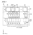
- Figure 1 is a layout showing an example of a position of a CAM region in a semiconductor integrated circuit according to the present invention.
- Figure 2 is a circuit diagram for explaining a structure of a conventional CAM circuit.
- Figure 3 is a circuit diagram showing the position of the conventional CAM circuit in a conventional memory device.
- Figure 4 is a circuit diagram for explaining that a pitch between the conventional CAM circuits is restricted by a position of main memory cells.
- Figure 5 is a layout of an example of a position of a conventional CAM region in a conventional semiconductor integrated circuit.
- Figure 6 is a layout of another example of the position of the conventional CAM region in the conventional semiconductor integrated circuit.
- Figure 1 shows an example of a layout of the CAM region 35 including CAM circuits and redundancy relief address comparison circults of a semiconductor integrated circuit according to the present invention.
- the CAM region 35 includes n first CAM circuits 30, m second CAM circuits 30' and n redundancy relief address comparison circuits 40 (hereinafter, each referred to as "comparison circuit 40" ).
- Each first CAM circuit 30 stores address information of the malfunctioning memory cell on which the redundancy relief is performed.
- Each second CAM circuit 30' stores information, such as a device code or the like, which is specific to the memory device and excludes the address information of the malfunctioning memory cell.
- first CAM circuits 30 and the m second CAM circuits 30' are provided such that the first CAM circuits 30 and the second CAM circuits 30' are alternately adjacent to each other and two adjacent comparison circuits 30 and 30' are spaced at a regular pitch p1 .
- the n comparison circuits 40 are provided along a direction parallel to a direction along which the CAM circuits 30 and 30' are provided, such that two adjacent comparison circuits 40 are spaced at a regular pitch p2 + W, where W denotes a width (not shown) of a conductor line 51 .
- W denotes a width (not shown) of a conductor line 51 .
- Each of the n first CAM circuits 30 is connected to a corresponding one of the n comparison circuits 40 by its respective n conductor line 50.
- Each of the m second CAM circuits 30' is connected to a corresponding buffer circuit or the like (not shown) by its respective m conductor line 51.
- the comparison circuit 40 has a function of comparing the address information of the malfunctioning memory cell stored in the first CAM circuit 30 to externally-input address information. When the comparison results in a mismatch, a voltage required to perform read/write operations or the like is applied to a word line connected to a memory cell corresponding to the externally-input address.
- the comparison circuit 40 is preferably positioned in the vicinity of the word line voltage control circuit 23 ( Figures 3 and 4 ).
- the CAM circuit 30' does not store the address information of the malfunctioning memory cell, and therefore unlike the comparison circuit 40, the buffer circuit or the like connected to the CAM circuit 30 is not severely restricted in its position and can be positioned away from the word line voltage control circuit 23 .
- the CAM circuits 30, which store the address information required for performing the redundancy relief on the flash memory and have outputs connected to a corresponding one of the comparison circuits 40, and the second CAM circuits 30', which store the information specific to the memory device, are alternately positioned so as to be adjacent to one another.
- the pitch between two adjacent first CAM circuits 30 and the pitch between two adjacent comparison circuits 40 can be made substantially the same such that corresponding pairs of the first CAM circuit 30 and the comparison circuit 40 can be connected together by the straight conductor lines 50 .
- the conductor line 51 for connecting the second CAM circuit 30' and the buffer circuit or the like can be provided so as to pass through a gap between the adjacent comparison circuits 40, and therefore there is no need to keep spaces so as to provide prescribed pitches between the adjacent conductor lines 51, i.e., the comparison circuit 40 fills each space between the adjacent conductor lines 51 in a region 61 shown in Figure 1 .
- an area of the CAM region 60 in which the first CAM circuits 30 and the second CAM circuits 30' are alternately positioned so as to be adjacent to one another and an area of the CAM region 60' ( Figure 6 ) in which the first CAM circuits 30 and the second CAM circuits 30' are separately positioned are determined by length x1 along the x direction and length y1 along they direction of the CAM circuits 30 and 30', the number n of the CAM circuits 30 and the number m of the CAM circuits 30' , and therefore the areas of the regions 60 and 60' are substantially the same.
- the conductor lines 51 in the region 61' shown in Figure 6 are spaced at a pitch P .
- a width of each of the conductor lines 51 shown in Figure 6 and the conductor lines 51 is represented by W
- a length along they direction of the comparison circuit 40 is represented by y2
- a pitch between the comparison circuits 40 is represented by p2
- W and P are positive numbers and satisfy the relationship P > W, and therefore the area of the region 61 is smaller than that of the region 61' by an area corresponding to a difference between the entire width of the conductor lines 51 and the entire space provided due to the pitches P between the adjacent conductor lines 51 .
- pitches P between the conductor lines are required along the y direction, and therefore the area of the conductor region 62 shown in Figure 1 is smaller than that of the conductor region 62' .
- the present invention by alternately positioning the first and second CAM circuits 30 and 30' so as to be adjacent to one another, it is possible to reduce the entire area of the CAM region.
- n and m are equal to each other
- the same effects can also be achieved in the case where the n and m are not equal to each other.
- the equal number of the first and second CAM circuits 30 and 30' are alternately positioned and the remaining first or second CAM circuits 30 or 30' are positioned together.
- both the pitches between the adjacent conductor lines 50 connected to the first CAM circuit 30 and the pitches between the adjacent conductor lines 51 connected to the second CAM circuits 30' are p1 which is greater than the minimum value P for a pitch determined by the necessities of the semiconductor production process, and therefore it is not necessary to further increase the pitches between the conductor lines 50 and 51 which are provided in the same layer of the circuit.
- each CAM circuit is used as an output circuit block and each comparison circuit is used as an input circuit block
- the present invention is not limited to such a configuration and is widely applicable to typical semiconductor integrated circuits including output circuit blocks and the input circuit blocks which are connected together by the conduotor lines.
- the present invention even when the pitch between the adjacent CAM circuits is different from that between the adjacent comparison circuits, by alternately positioning the first CAM circuits connected tc the comparison circuits and the second CAM circuits connected to the buffer circuits or the like, it is possible to connect the first CAM circuits to the comparison circuits by conductor lines which are kept straight. Accordingly, as compared to the conventional technique using the conductor lines which are required to be bent so as to connect the circuit blocks together, according to the present invention, it is possible to reduce the load provided on the conductor lines by shortening the length thereof and prevent the size of the semiconductor integrated circuit from being increased along the y direction as shown in the drawings, e.g., Figure 1.
Landscapes
- Semiconductor Integrated Circuits (AREA)
- For Increasing The Reliability Of Semiconductor Memories (AREA)
- Semiconductor Memories (AREA)
- Internal Circuitry In Semiconductor Integrated Circuit Devices (AREA)
Abstract
Description
Claims (8)
- A semiconductor integrated circuit comprising:n first output circuit blocks and m second output circuit blocks which are provided such that adjacent first and second output circuit blocks are spaced at a regular first pitch; andn input circuit blocks provided parallel to a direction along which the first and second output circuit blocks are provided, the input circuit blocks being provided such that adjacent input circuit blocks are spaced at a regular second pitch,wherein the first and second output circuit blocks are provided such that at least part of ones of the first and second output circuit blocks alternate with the other ones of the first and second output circuit blocks and each of the first output circuit blocks is connected to a corresponding one of input circuit blocks by a first conductor line such that a length of the first conductor line is shortest between the first output circuit blocks and the corresponding ones of input circuit blocks, andsecond conductor lines are connected to the second output circuit blocks such that each second conductor line passes through a gap between the input circuit blocks.
- A semiconductor integrated circuit according to claim 1, wherein layouts of the first and second output circuit blocks are identical.
- A semiconductor integrated circuit according to claim 1, wherein:the semiconductor integrated circuit has a redundancy relief function for substituting a normal spare memory cell for a malfunctioning memory cell;each of the first output circuit blocks is a memory circuit for storing address information of the malfunctioning memory cell;each of the input circuit blocks is a comparison circuit for comparing the address information stored in the memory circuit and externally-input address information in which when the comparison results in a mismatch, access to a memory cell corresponding to the externally-input address is performed and when the comparison results in a match, access to the spare memory cell is performed.
- A semiconductor integrated circuit according to claim 1, wherein the second pitch is twice as long as the first pitch.
- A semiconductor integrated circuit according to claim 2, wherein:the semiconductor integrated circuit has a redundancy relief function for substituting a normal spare memory cell for a malfunctioning memory cell;each of the first output circuit blocks is a memory circuit for storing address information of the malfunctioning memory cell;each of the input circuit blocks is a comparison circuit for comparing the address information stored in the memory circuit and externally-input address information in which when the comparison results in a mismatch, access to a memory cell corresponding to the externally-input address is performed and when the comparison results in a match, access to the spare memory cell is performed.
- A semiconductor integrated circuit according to claim 2, wherein the second pitch is twice as long as the first pitch.
- A semiconductor integrated circuit according to claim 3, wherein the second pitch is twice as long as the first pitch.
- A semiconductor integrated circuit according to claim 5, wherein the second pitch is twice as long as the first pitch.
Applications Claiming Priority (2)
| Application Number | Priority Date | Filing Date | Title |
|---|---|---|---|
| JP2001192712A JP3815717B2 (en) | 2001-06-26 | 2001-06-26 | Semiconductor integrated circuit |
| JP2001192712 | 2001-06-26 |
Publications (3)
| Publication Number | Publication Date |
|---|---|
| EP1278204A2 true EP1278204A2 (en) | 2003-01-22 |
| EP1278204A3 EP1278204A3 (en) | 2005-10-19 |
| EP1278204B1 EP1278204B1 (en) | 2015-12-23 |
Family
ID=19031126
Family Applications (1)
| Application Number | Title | Priority Date | Filing Date |
|---|---|---|---|
| EP02254341.7A Expired - Lifetime EP1278204B1 (en) | 2001-06-26 | 2002-06-21 | Semiconductor integrated circuit |
Country Status (5)
| Country | Link |
|---|---|
| US (1) | US6661692B2 (en) |
| EP (1) | EP1278204B1 (en) |
| JP (1) | JP3815717B2 (en) |
| KR (1) | KR100451009B1 (en) |
| TW (1) | TW559825B (en) |
Families Citing this family (5)
| Publication number | Priority date | Publication date | Assignee | Title |
|---|---|---|---|---|
| KR100624287B1 (en) * | 2004-05-11 | 2006-09-18 | 에스티마이크로일렉트로닉스 엔.브이. | Redundancy Circuit for NAND Flash Memory Devices |
| US7638850B2 (en) | 2004-10-14 | 2009-12-29 | Saifun Semiconductors Ltd. | Non-volatile memory structure and method of fabrication |
| EP1746645A3 (en) * | 2005-07-18 | 2009-01-21 | Saifun Semiconductors Ltd. | Memory array with sub-minimum feature size word line spacing and method of fabrication |
| KR100823706B1 (en) * | 2006-07-21 | 2008-04-21 | 삼성전자주식회사 | Signal line structure of a semiconductor device and method of manufacturing the same |
| DE102017127276A1 (en) * | 2017-08-30 | 2019-02-28 | Taiwan Semiconductor Manufacturing Co., Ltd. | STANDARD CELLS AND ADAPTATIONS FROM THEREOF WITHIN A STANDARD CELL LIBRARY |
Family Cites Families (9)
| Publication number | Priority date | Publication date | Assignee | Title |
|---|---|---|---|---|
| JPS5835963A (en) * | 1981-08-28 | 1983-03-02 | Fujitsu Ltd | Integrated circuit device |
| DE69024427T2 (en) * | 1989-08-30 | 1996-07-18 | Nippon Electric Co | Semiconductor memory device |
| US5150330A (en) * | 1990-01-24 | 1992-09-22 | Vlsi Technology, Inc. | Interblock dispersed-word memory architecture |
| JP2590712B2 (en) | 1993-12-02 | 1997-03-12 | 日本電気株式会社 | Memory controller |
| TW332923B (en) * | 1996-04-19 | 1998-06-01 | Matsushita Electric Industrial Co Ltd | Semiconductor IC |
| JP3597706B2 (en) * | 1997-07-25 | 2004-12-08 | 株式会社東芝 | Logic embedded memory |
| JP3092558B2 (en) * | 1997-09-16 | 2000-09-25 | 日本電気株式会社 | Semiconductor integrated circuit device |
| JP3469074B2 (en) * | 1997-12-12 | 2003-11-25 | 株式会社東芝 | Semiconductor memory device |
| JP2001077322A (en) * | 1999-09-02 | 2001-03-23 | Toshiba Corp | Semiconductor integrated circuit device |
-
2001
- 2001-06-26 JP JP2001192712A patent/JP3815717B2/en not_active Expired - Fee Related
-
2002
- 2002-06-21 EP EP02254341.7A patent/EP1278204B1/en not_active Expired - Lifetime
- 2002-06-24 US US10/179,710 patent/US6661692B2/en not_active Expired - Lifetime
- 2002-06-25 TW TW091113871A patent/TW559825B/en not_active IP Right Cessation
- 2002-06-26 KR KR10-2002-0035968A patent/KR100451009B1/en not_active Expired - Fee Related
Also Published As
| Publication number | Publication date |
|---|---|
| KR100451009B1 (en) | 2004-10-02 |
| TW559825B (en) | 2003-11-01 |
| EP1278204B1 (en) | 2015-12-23 |
| US6661692B2 (en) | 2003-12-09 |
| KR20030004066A (en) | 2003-01-14 |
| JP2003007079A (en) | 2003-01-10 |
| US20030011004A1 (en) | 2003-01-16 |
| JP3815717B2 (en) | 2006-08-30 |
| EP1278204A3 (en) | 2005-10-19 |
Similar Documents
| Publication | Publication Date | Title |
|---|---|---|
| US7177173B2 (en) | Pattern layout of word line transfer transistors in NAND flash memory which executes subblock erase | |
| US7505318B2 (en) | Nonvolatile semiconductor memory device | |
| KR102123736B1 (en) | Semiconductor memory device | |
| US20250118354A1 (en) | Semiconductor memory device having memory chip bonded to a cmos chip including a peripheral circuit | |
| JP2635810B2 (en) | Semiconductor storage device | |
| US6822900B2 (en) | Non-volatile semiconductor memory device | |
| US10559350B2 (en) | Memory circuit and electronic device | |
| US7274617B2 (en) | Non-volatile semiconductor memory | |
| TWI802199B (en) | semiconductor memory device | |
| US20080123424A1 (en) | Non-volatile semiconductor memory device | |
| US20100328985A1 (en) | Semiconductor device having plural circuit blocks laid out in a matrix form | |
| US5637895A (en) | Non-volatile semiconductor memory device | |
| US6016265A (en) | Fuse-latch circuit having high integration density | |
| JP3559415B2 (en) | Semiconductor storage device | |
| US6661692B2 (en) | Semiconductor integrated circuit | |
| US7142453B2 (en) | Semiconductor memory device and memory card | |
| US7541654B2 (en) | Semiconductor memory device and semiconductor device including multilayer gate electrode | |
| JP2009141222A (en) | Semiconductor integrated circuit device | |
| US7167393B2 (en) | Nonvolatile semiconductor memory device containing reference capacitor circuit | |
| US6606268B2 (en) | Non-volatile semiconductor integrated circuit | |
| US7463518B2 (en) | Layout structure for use in flash memory device | |
| KR20070021758A (en) | X-Decoder of NAND Flash Memory and Its Decoder Placement Method | |
| JP4033438B2 (en) | Semiconductor memory device | |
| JPH11177059A (en) | Semiconductor memory device | |
| JP4634973B2 (en) | Semiconductor memory device |
Legal Events
| Date | Code | Title | Description |
|---|---|---|---|
| PUAI | Public reference made under article 153(3) epc to a published international application that has entered the european phase |
Free format text: ORIGINAL CODE: 0009012 |
|
| AK | Designated contracting states |
Kind code of ref document: A2 Designated state(s): AT BE CH CY DE DK ES FI FR GB GR IE IT LI LU MC NL PT SE TR |
|
| AX | Request for extension of the european patent |
Free format text: AL;LT;LV;MK;RO;SI |
|
| PUAL | Search report despatched |
Free format text: ORIGINAL CODE: 0009013 |
|
| AK | Designated contracting states |
Kind code of ref document: A3 Designated state(s): AT BE CH CY DE DK ES FI FR GB GR IE IT LI LU MC NL PT SE TR |
|
| AX | Request for extension of the european patent |
Extension state: AL LT LV MK RO SI |
|
| RIC1 | Information provided on ipc code assigned before grant |
Ipc: 7H 01L 27/02 B Ipc: 7G 11C 5/02 A Ipc: 7G 11C 29/00 B |
|
| 17P | Request for examination filed |
Effective date: 20060331 |
|
| AKX | Designation fees paid |
Designated state(s): DE FR GB IT NL |
|
| 17Q | First examination report despatched |
Effective date: 20071123 |
|
| RAP1 | Party data changed (applicant data changed or rights of an application transferred) |
Owner name: INTELLECTUAL PROPERTIES I KFT. |
|
| RAP1 | Party data changed (applicant data changed or rights of an application transferred) |
Owner name: SAMSUNG ELECTRONICS CO., LTD. |
|
| GRAP | Despatch of communication of intention to grant a patent |
Free format text: ORIGINAL CODE: EPIDOSNIGR1 |
|
| INTG | Intention to grant announced |
Effective date: 20150616 |
|
| GRAS | Grant fee paid |
Free format text: ORIGINAL CODE: EPIDOSNIGR3 |
|
| GRAA | (expected) grant |
Free format text: ORIGINAL CODE: 0009210 |
|
| AK | Designated contracting states |
Kind code of ref document: B1 Designated state(s): DE FR GB IT NL |
|
| REG | Reference to a national code |
Ref country code: GB Ref legal event code: FG4D |
|
| REG | Reference to a national code |
Ref country code: DE Ref legal event code: R096 Ref document number: 60247683 Country of ref document: DE |
|
| REG | Reference to a national code |
Ref country code: NL Ref legal event code: MP Effective date: 20151223 |
|
| PG25 | Lapsed in a contracting state [announced via postgrant information from national office to epo] |
Ref country code: NL Free format text: LAPSE BECAUSE OF FAILURE TO SUBMIT A TRANSLATION OF THE DESCRIPTION OR TO PAY THE FEE WITHIN THE PRESCRIBED TIME-LIMIT Effective date: 20151223 |
|
| PG25 | Lapsed in a contracting state [announced via postgrant information from national office to epo] |
Ref country code: IT Free format text: LAPSE BECAUSE OF FAILURE TO SUBMIT A TRANSLATION OF THE DESCRIPTION OR TO PAY THE FEE WITHIN THE PRESCRIBED TIME-LIMIT Effective date: 20151223 |
|
| REG | Reference to a national code |
Ref country code: DE Ref legal event code: R097 Ref document number: 60247683 Country of ref document: DE |
|
| PLBE | No opposition filed within time limit |
Free format text: ORIGINAL CODE: 0009261 |
|
| STAA | Information on the status of an ep patent application or granted ep patent |
Free format text: STATUS: NO OPPOSITION FILED WITHIN TIME LIMIT |
|
| 26N | No opposition filed |
Effective date: 20160926 |
|
| GBPC | Gb: european patent ceased through non-payment of renewal fee |
Effective date: 20160621 |
|
| REG | Reference to a national code |
Ref country code: FR Ref legal event code: ST Effective date: 20170228 |
|
| PG25 | Lapsed in a contracting state [announced via postgrant information from national office to epo] |
Ref country code: FR Free format text: LAPSE BECAUSE OF NON-PAYMENT OF DUE FEES Effective date: 20160630 |
|
| PG25 | Lapsed in a contracting state [announced via postgrant information from national office to epo] |
Ref country code: GB Free format text: LAPSE BECAUSE OF NON-PAYMENT OF DUE FEES Effective date: 20160621 |
|
| PGFP | Annual fee paid to national office [announced via postgrant information from national office to epo] |
Ref country code: DE Payment date: 20210525 Year of fee payment: 20 |
|
| REG | Reference to a national code |
Ref country code: DE Ref legal event code: R071 Ref document number: 60247683 Country of ref document: DE |