EP1278155A2 - Card device comprising an antenna and connected with an electronic apparatus or a wireless device - Google Patents
Card device comprising an antenna and connected with an electronic apparatus or a wireless device Download PDFInfo
- Publication number
- EP1278155A2 EP1278155A2 EP02015168A EP02015168A EP1278155A2 EP 1278155 A2 EP1278155 A2 EP 1278155A2 EP 02015168 A EP02015168 A EP 02015168A EP 02015168 A EP02015168 A EP 02015168A EP 1278155 A2 EP1278155 A2 EP 1278155A2
- Authority
- EP
- European Patent Office
- Prior art keywords
- antenna
- wireless device
- electronic apparatus
- coupling element
- card
- Prior art date
- Legal status (The legal status is an assumption and is not a legal conclusion. Google has not performed a legal analysis and makes no representation as to the accuracy of the status listed.)
- Granted
Links
Images


Classifications
-
- H—ELECTRICITY
- H01—ELECTRIC ELEMENTS
- H01Q—ANTENNAS, i.e. RADIO AERIALS
- H01Q1/00—Details of, or arrangements associated with, antennas
- H01Q1/12—Supports; Mounting means
- H01Q1/22—Supports; Mounting means by structural association with other equipment or articles
-
- H—ELECTRICITY
- H01—ELECTRIC ELEMENTS
- H01Q—ANTENNAS, i.e. RADIO AERIALS
- H01Q1/00—Details of, or arrangements associated with, antennas
- H01Q1/36—Structural form of radiating elements, e.g. cone, spiral, umbrella; Particular materials used therewith
- H01Q1/38—Structural form of radiating elements, e.g. cone, spiral, umbrella; Particular materials used therewith formed by a conductive layer on an insulating support
Definitions
- the present invention relates to a small-sized card device to be detachably inserted into a slot of an electronic apparatus and, particularly, to a wireless device wherein effects of diversity can be obtained even with a small size.
- wireless devices such as card devices which comprise antennas and provide electronic apparatuses with wireless communications functions have been widely used.
- Card devices of this type are typified by wireless LAN cards, card-type modems and the like.
- card devices for the addition of wireless communications functions simultaneously with the addition of system resources such as memories are provided.
- the present invention covers any type of wireless device as long as the wireless device is equipped with an antenna.
- wireless devices of this type include devices that have a plurality of antennas and in that antenna diversity has been realized. With such a construction, antenna diversity relieves harmful influences due to phasing and, accordingly, a satisfactory communications condition is easily obtained, which is preferable.
- a space diversity scheme wherein two or more antennas are arranged so as to be physically separated and one of the antennas with the superior communications condition is selected. Namely, a contrivance has been made so that, by separating the antenna positions, the antennas are not electrically coupled to each other and the individual antennas have unique radiation characteristics.
- a card device is to be inserted into a slot of an electronic apparatus having an electronic apparatus ground and electrically connected to this electronic apparatus and comprises:
- radiation characteristics of an antenna depend on characteristics of the antenna itself, a card ground pattern and the like, however, if a card ground is connected to an electronic apparatus ground with a high frequency, radiation characteristics of the antenna are influenced by the electronic apparatus ground.
- two types of radiation characteristics can be selected by only the single antenna, effects similar to those of antenna diversity can be obtained, whereby communications states can be improved.
- a reduction in size of the card device can be promoted in reality.
- a card device according to the second aspect of the invention comprises:
- the card device itself selects a more preferable condition, therefore, convenience can be improved.
- the card device since it is unnecessary to control an antenna changeover at the electronic apparatus side, no additional load is imposed on the electronic apparatus.
- the antenna is a w1/4 chip antenna exposed outside the carrier.
- a wireless device according to the fifth aspect of the invention comprises:
- a wireless device according to the sixth aspect of the invention comprises:
- the present invention has tried to make use of such electrical coupling to the contrary and has revealed that by changing the degree of electrical coupling, a plurality of radiation characteristics can be obtained per one antenna (that is, effects of diversity can be provided), which will be described later in the section of embodiments.
- variable impedance device varies impedance between the two levels of high impedance and low impedance.
- variable impedance device can be a simple switch (with ON, the impedance is 0: with OFF, the impedance is infinite).
- the coupling element is an antenna element to which no electrical power is fed.
- the coupling element can be provided as a component of the same type as the antenna, therefore, the number of component types can be reduced, whereby a reduction in costs can be realized.
- the coupling element is a circuit pattern.
- the coupling element is a component of an electronic apparatus to which this wireless device is attached.
- a wireless device according to the thirteenth aspect of the invention comprises:
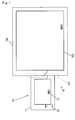
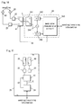
- Fig. 1 is a schematic plan view of a card device and an electronic apparatus according to Embodiment 1 of the present invention.
- a card device 10 is detachably inserted (in the direction of arrow N1) into a slot 101 of an electronic apparatus 100, thereby providing the electronic apparatus 100 with wireless communications functions.
- electronic apparatuses 100 a variety of information processing units such as personal computers (either laptops or desktops will suffice), personal digital assistants (PDAs), digital cameras and the like can be considered.
- PDAs personal digital assistants
- these electronic apparatuses 100 have electronic apparatus grounds 102 inside thereof.
- the electronic apparatus grounds 102 vary in size, etc., depending on the individual apparatuses, and in general, whether or not the electronic apparatus ground 102 contributes to an improvement in characteristics of the antenna 12 or the degree of contribution is unknown.
- the card device 10 has a carrier 11 formed into a card shape and a single antenna 12 provided on the carrier 11.
- the antenna 12 where the wavelength of a radio wave to be used for communications is provided as w1
- a w1/4 chip antenna is used. According thereto, a reduction in size of the card device can be easily carried out, therefore, this is convenient.
- the antenna 12 can also be constructed by a circuit pattern.
- the card device 10 also has a card ground 13 inside the carrier 11.
- the card ground 13 and the electronic apparatus ground 102 are formed as circuit patterns on a printed circuit board.
- a printed circuit board is provided inside the carrier 11.
- Fig. 2 is a functional block diagram of the card device according to Embodiment 1 of the present invention.
- a switch 14 connects/disconnects, with a high frequency, between the card ground 13 and electronic apparatus ground 10 in response to a changeover signal from a control unit 17.
- the card ground 13 and the electronic apparatus ground 102 are conductive to each other in terms of a direct current.
- a demodulating unit 15 accepts a signal received by the antenna 12 for demodulation and outputs the demodulated signal to a judging unit 16.
- the judging unit 16 accepts the demodulated signal of the demodulating unit 15 and judges whether or not the communications state by the current antenna 12 is satisfactory.
- any criterion such as a bit error rate, a cyclic redundancy check (CRC), intensity of the demodulated signal or the like can be arbitrarily selected as long as it can be an objective indicator of the communications state of the antenna 12.
- CRC cyclic redundancy check
- the control unit 17 is for controlling the demodulating unit 15, the judging unit 16, the switch 14 and the like, and this control unit 17 stores judgment results of the judging unit 16 in a memory 18 and also outputs, with reference to the information stored in the memory 18, a changeover signal to the switch 14 so as to reach a more preferable communications condition.
- control unit 17 may output, with reference to the information of the memory 18, a changeover signal to the switch 14 so as to maintain one condition at all times, or alternatively, when communications are carried out by use of a plurality of channels with different frequencies, the control unit 17 may change over the switch 14 for each channel, if necessary.
- Embodiment 1 the demodulating unit 15, the judging unit 16, the control unit 17, and the memory 18 correspond to a wireless module in Embodiments 2 and 3.
- this wireless device comprises an antenna and a coupling element which is electrically coupled to this antenna.
- the antenna and coupling element are intentionally electrically coupled to each other. Then, the degree of coupling is varied.
- Fig. 3 is a block diagram of the wireless device according to Embodiment 2 of the present invention.
- an antenna 20 and a coupling element 21 are arranged in contiguity with each other, and the coupling element 21 is electrically coupled to the antenna 20.
- the antenna 20 is not necessarily a special antenna and, for example, when the frequency band is approximately 2.4GHz or 5GHz and a small-sized wireless device is constructed, a surface-mounting laminated ceramic chip antenna, micro-strip line antenna, patch antenna, spiral antenna or the like can be used.
- a component whose specifications are clear at the design phase (such as an antenna similar to the antenna 20) is desirable, however, a component whose specifications are unclear at the design phase (such as a component of an electronic apparatus to which this wireless device is attached) may also be used.
- a crucial point in the present embodiment is that while electrical power feeding is carried out to the antenna 20 for information communications, such electrical power feeding is not carried out to a coupling element 21. Accordingly, even if a part that originally assumes use as an antenna is used, this part does not act as an antenna but consistently acts only as a coupling element to be coupled to the antenna 20.
- a matching circuit 22 is connected, and after the coupling element 21, a matching circuit 23 is connected.
- These matching circuits 22 and 23 contain respective filters.
- a wireless module 24 is connected via a feed line L.
- a variable impedance device 25 is connected, and the variable impedance device 25 is further connected to a ground point of the wireless device.
- the variable impedance device 25 determines an impedance between the coupling element 21 and ground point.
- a switch for varying impedance between the two levels of high impedance (impedance: infinite) and low impedance (impedance: 0) is used as the variable impedance device 25.
- variable impedance device 25 may be constructed by an impedance bridge or a variable resistance, and with this construction, the impedance can be varied among a greater number of levels or without levels, thus a greater number of types of radiation characteristics can be obtained.
- the wireless module 24 has the following factors. First, a switch 241 alternatively changes over the feed line L between the sending side and receiving side. To the sending side, an output terminal of a power amplifier 242 is connected, and to the receiving side, an input terminal of a low-noise amplifier 243 is connected. In addition, to the power amplifier 242 and low-noise amplifier 243, a power source 244 is connected.
- the wireless module 24 comprises a modulator/demodulator circuit 245, and this modulator/demodulator circuit 245, during sending, modulates sending information obtained from the outside of the wireless device and outputs the information to the power amplifier 242, and, during receiving, demodulates the waveform obtained from the low-noise amplifier 243 and outputs the receiving information to the outside of the wireless device.
- the modulator/demodulator circuit 245 outputs an impedance control signal S1 to the variable impedance device 25 and controls an impedance between the coupling element 21 and ground point. Namely, if this immediate control signal S1 is changed, radiation characteristics of the antenna 20 are changed.
- a laminated ceramic chip antenna 211 is used as the antenna 20. Then, on one side of a printed circuit board 26, the antenna 20 and the laminated ceramic chip antenna 211 are arranged in contiguity with each other so that the laminated ceramic chip antenna 211 and the antenna 20 are electrically coupled to each other.
- the size of the printed circuit board 26 is 50mm long and 25mm wide, and as the antenna 20 and the laminated ceramic chip antenna 211, an antenna with a model number YCE-5208 manufactured by YOKOWO, Co.,Ltd. was used, and as the variable impedance device 25, a switch with a model number UPG152TA manufactured by NEC Corporation was used.
- a measurement was carried out by using a 2.44GHz-frequency with a height of 2.5m from the floor surface and a 4m-distance from the receiving side and with a wireless device according to this mounting example arranged on the sending side.
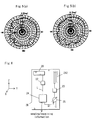
- Fig. 5(a) shows radiation characteristics of the antenna 20 resulting from a measurement with the switch opened (that is, the impedance is infinite), wherein the direction of 0[deg] is the X-direction, and the direction of -90[deg] is the Y-direction.
- Fig. 5(b) shows a result of a measurement with the switch closed (that is, the impedance is 0).
- a micro-strip line antenna formed by a circuit pattern of the printed circuit board 26 was used.
- Other aspects were identical to those of Mounting Example 1 and a measurement example thereof is as shown in Fig. 7(a) and Fig. 7(b).
- connection point 213 having conductivity is provided on the side of the printed circuit board 26, and the variable impedance device 25 is connected to this connection point 213. Then, when this wireless device is attached to an electronic apparatus such as a personal computer and used, the variable impedance device 25 is connected to this electronic apparatus ground 102 via the connection point 213.
- the present invention can also be applied to a headphone 30 having an inverse U-shaped belt portion 33 and two pad portions 31 and 32 to be fixed to both ends thereof.
- a headphone 30 is provided with a metal wire frame 311, in general, inside the belt portion 33 for reinforcement or other purposes.
- connection point 213 on the print circuit wire 26 it is satisfactory to provide a member similar to the connection point 213 on the print circuit wire 26 and electrically connect this connection point 213 to the wire frame 331.
- Fig. 10 is a block diagram of a wireless device according to Embodiment 3 of the present invention.
- components identical to those of Embodiment 2 are signified by identical symbols, whereby a description thereof will be omitted.
- two surface-mounting antennas 20 and 40 are arranged in contiguity with each other on one side of the printed circuit board 26, whereby these antennas 20 and 40 are electrically coupled to each other.
- the antennas 20 and 40 are not necessarily special antennas and, for example, when the frequency band is approximately 2.4GHz or 5GHz and a small-sized wireless device is constructed, surface-mounting laminated ceramic chip antennas, micro-strip line antennas, patch antennas, spiral antennas or the like can be used.
- an antenna changeover signal S2 is outputted from the modulator/demodulator circuit 245 to an antenna switch 41.
- the antenna switch 41 alternatively selects an antenna for use for communications out of these antennas 20 and 40 in accordance with the antenna changeover signal S2.
- the selected antenna (including the antenna 40) is fed with electrical power from the feed line L, and thereby acts as an antenna.
- the surface-mounting antennas are arranged on one surface of the circuit board in a concentrated fashion, therefore, a thin wireless device can be constructed.
Landscapes
- Support Of Aerials (AREA)
- Variable-Direction Aerials And Aerial Arrays (AREA)
- Coupling Device And Connection With Printed Circuit (AREA)
- Transceivers (AREA)
Abstract
Description
- The present invention relates to a small-sized card device to be detachably inserted into a slot of an electronic apparatus and, particularly, to a wireless device wherein effects of diversity can be obtained even with a small size.
- In recent years, wireless devices such as card devices which comprise antennas and provide electronic apparatuses with wireless communications functions have been widely used. Card devices of this type are typified by wireless LAN cards, card-type modems and the like. In addition, card devices for the addition of wireless communications functions simultaneously with the addition of system resources such as memories are provided. The present invention covers any type of wireless device as long as the wireless device is equipped with an antenna.
- In addition, wireless devices of this type include devices that have a plurality of antennas and in that antenna diversity has been realized. With such a construction, antenna diversity relieves harmful influences due to phasing and, accordingly, a satisfactory communications condition is easily obtained, which is preferable.
- In further detail, a space diversity scheme is used, wherein two or more antennas are arranged so as to be physically separated and one of the antennas with the superior communications condition is selected. Namely, a contrivance has been made so that, by separating the antenna positions, the antennas are not electrically coupled to each other and the individual antennas have unique radiation characteristics.
- As wireless devices of this type, smaller and lighter wireless devices have been demanded. Herein, for example, when a radio wave having a 2.4GHz band is used, it is possible to mount two antennas on wireless devices as long as they approximate the size of Personal Computer Memory Card International Association (PCMCIA) cards or less.
- However, if the size becomes smaller than this size, for reasons concerning space, etc., it is in reality difficult to mount two antennas in a separate fashion, and in most cases, only one antenna can be mounted. In these cases, no effects of the space diversity are obtained.
- In regard hereto, wireless devices having small-sized chips as antennas have been put into market circulation, however, even if such small-sized antennas are used, problems similar to the foregoing exist.
- Therefore, it is an object of the present invention to provide a card device in which, while a single antenna is used, effects similar to those of antenna diversity can also be obtained.
- In addition, it is another object of the present invention to provide a wireless device in which effects of diversity can be obtained even with a small size where effects of space diversity have been hardly obtained.
- A card device according to the first aspect of the invention is to be inserted into a slot of an electronic apparatus having an electronic apparatus ground and electrically connected to this electronic apparatus and comprises:
- a carrier,
- a single antenna provided on the carrier,
- a card ground which is disposed in the carrier and electrically connected to the antenna, and
- a switch for carrying out, with a high frequency, a connection/disconnection of the card ground to/from the electronic apparatus ground in a condition where this card device is inserted in the slot.
-
- In this construction, even with only a single antenna, two types of radiation characteristics concerning
- (1)a condition where the card ground and the electronic apparatus ground are connected with a high frequency and in
- (2)a condition where the card ground and the electric apparatus ground are disconnected with a high frequency can be obtained by changing over the switch.
-
- Herein, in general, radiation characteristics of an antenna depend on characteristics of the antenna itself, a card ground pattern and the like, however, if a card ground is connected to an electronic apparatus ground with a high frequency, radiation characteristics of the antenna are influenced by the electronic apparatus ground.
- It is not necessarily appropriate to determine which of these two conditions is more preferable, however, in a case where the electronic apparatus ground successfully resonates, an improvement in the antenna performance (antenna gain, directivity, etc.) can be expected in the connected condition rather than in the disconnected condition.
- As such, two types of radiation characteristics can be selected by only the single antenna, effects similar to those of antenna diversity can be obtained, whereby communications states can be improved. In addition, accordingly, a reduction in size of the card device can be promoted in reality.
- A card device according to the second aspect of the invention comprises:
- a demodulating unit which accepts a signal received by the antenna for demodulation,
- a judging unit which accepts the signal demodulated by the demodulating unit and judges the quality of the communications state of the antenna, and
- a control unit for controlling the switch with reference to the judgment result of the judging unit.
-
- With this construction, the card device itself selects a more preferable condition, therefore, convenience can be improved. In addition, since it is unnecessary to control an antenna changeover at the electronic apparatus side, no additional load is imposed on the electronic apparatus.
- In a card device according to the third aspect of the invention, the antenna is a w1/4 chip antenna exposed outside the carrier.
- With this construction, a reduction in size of the card device can be more easily carried out. In this antenna, a material having a high dielectric constant is used, and where a relative dielectric constant is dcrp, a reduction in size to w1/4 √(dcrp) can be achieved.
- A wireless device according to the fifth aspect of the invention comprises:
- an antenna and a coupling element which is electrically coupled to this antenna, wherein
- electrical characteristics of the coupling element are made variable, so that a plurality of radiation characteristics can be obtained by the antenna.
-
- A wireless device according to the sixth aspect of the invention comprises:
- an antenna,
- a wireless module which feeds electrical power to the antenna and transmits information via the antenna,
- a coupling element which is arranged in contiguity with the antenna and
- electrically coupled to the antenna, and
- a variable impedance device provided between the coupling element and a ground point, wherein
- the wireless module operates the variable impedance device to change the impedance between the coupling element and ground point, so that a plurality of radiation characteristics are obtained by the antenna.
-
- In the prior arts, research has been carried out so that a plurality of antennas have respectively unique radiation characteristics, that is, in only a direction so as to avoid electrical coupling between antennas.
- In contrast thereto, the present invention has tried to make use of such electrical coupling to the contrary and has revealed that by changing the degree of electrical coupling, a plurality of radiation characteristics can be obtained per one antenna (that is, effects of diversity can be provided), which will be described later in the section of embodiments.
- Based on this knowledge, since the present invention carries out construction as in the above, merits are provided such that:
- (1) effects of diversity can be obtained without preparing a plurality of antennas.
- (2) only electrical characteristics of the coupling element are changed and the antenna itself is not changed over, therefore, unlike the normal antenna diversity, no instantaneous interruption of a path for receiving a signal from the antenna occurs.
- (3) it is unnecessary to excessively separate the antenna and coupling element (in the prior art, this element corresponds to another antenna in terms of the arrangement) and it is rather preferable that these are made approximate, therefore, the components can be laid out in a concentrated fashion, which is advantageous in a case where the components are mounted onto a small-sized wireless device.
-
- In a wireless device according to the seventh aspect of the invention, the variable impedance device varies impedance between the two levels of high impedance and low impedance.
- With this construction, two types of radiation characteristics can be obtained and effects of diversity can be obtained with a simple construction. For example, the variable impedance device can be a simple switch (with ON, the impedance is 0: with OFF, the impedance is infinite).
- In a wireless device according to the eighth aspect of the invention, the coupling element is an antenna element to which no electrical power is fed.
- With this construction, the coupling element can be provided as a component of the same type as the antenna, therefore, the number of component types can be reduced, whereby a reduction in costs can be realized.
- In a wireless device according to the ninth aspect of the invention, the coupling element is a circuit pattern.
- With this construction, an original constituent of a wireless device can be utilized as a coupling element, whereby a reduction in costs can be realized.
- In a wireless device according to the tenth aspect of the invention, the coupling element is a component of an electronic apparatus to which this wireless device is attached.
- With this construction, by diverting a component of an electronic apparatus into the coupling element, the number of components can be reduced, which is advantageous in terms of cost and layout.
- A wireless device according to the thirteenth aspect of the invention comprises:
- a substrate,
- a plurality of surface-mounting antennas which are arranged in contiguity with each other on one surface of the substrate and electrically coupled to each other,
- an antenna switch for alternatively selecting an antenna for use for communications out of these antennas, and
- a wireless module which outputs an antenna changeover signal to the antenna switch, feeds electrical power to an antenna selected by the antenna switch, and
- transmits information via this antenna.
-
- With this construction, even in a case where the mounting area of the antenna is narrow and effects of space diversity are hardly obtainable, effects of directional diversity can be obtained. In addition, since surface-mounting antennas are arranged on one surface of the substrate in a concentrated fashion, the thickness of the wireless device can be reduced.
- The above, and other objects, features and advantages of the present invention will become apparent from the following description read in conjunction with the accompanying drawings, in which like reference numerals designate the same elements.
-
- Fig. 1 is a schematic plan view of a card device and an electronic apparatus
according to
Embodiment 1 of the present invention, - Fig. 2 is a functional block diagram of the card device according to Embodiment I of the present invention,
- Fig. 3 is a block diagram of the wireless device according to
Embodiment 2 of the present invention, - Fig. 4 is a plan view of the wireless device according to
Embodiment 2 of the present invention, - Fig. 5(a) and Fig. 5(b) are graphs showing radiation characteristics of the
antenna according to
Embodiment 2 of the present invention, - Fig. 6 is a plan view of a wireless device according to
Embodiment 2 of the present invention, - Fig. 7(a) and Fig. 7(b) are graphs showing radiation characteristics of the
antenna according to
Embodiment 2 of the present invention, - Fig. 8 is a plan view of the wireless device according to
Embodiment 2 of the present invention, - Fig. 9(a) is a front view of a headphone provided with the wireless device
according to
Embodiment 2 of the present invention, - Fig. 9(b) is a partially enlarged view of the same headphone,
- Fig. 10 is a block diagram of the wireless device according to Embodiment 3 of the present invention, and
- Fig. 11 is a plan view of the wireless device according to Embodiment 3 of the present invention.
-
- Hereinafter, embodiments of the present invention will be described with reference to the drawings.
- Fig. 1 is a schematic plan view of a card device and an electronic apparatus according to
Embodiment 1 of the present invention. - As shown in Fig. 1, a
card device 10 is detachably inserted (in the direction of arrow N1) into aslot 101 of anelectronic apparatus 100, thereby providing theelectronic apparatus 100 with wireless communications functions. - Herein, as
electronic apparatuses 100, a variety of information processing units such as personal computers (either laptops or desktops will suffice), personal digital assistants (PDAs), digital cameras and the like can be considered. - And, these
electronic apparatuses 100 haveelectronic apparatus grounds 102 inside thereof. However, theelectronic apparatus grounds 102 vary in size, etc., depending on the individual apparatuses, and in general, whether or not theelectronic apparatus ground 102 contributes to an improvement in characteristics of theantenna 12 or the degree of contribution is unknown. - In addition, the
card device 10 has acarrier 11 formed into a card shape and asingle antenna 12 provided on thecarrier 11. Herein, as theantenna 12, where the wavelength of a radio wave to be used for communications is provided as w1, a w1/4 chip antenna is used. According thereto, a reduction in size of the card device can be easily carried out, therefore, this is convenient. - Moreover, in place thereof, the
antenna 12 can also be constructed by a circuit pattern. Similar to theelectronic apparatus 100, thecard device 10 also has acard ground 13 inside thecarrier 11. In addition, in general, thecard ground 13 and theelectronic apparatus ground 102 are formed as circuit patterns on a printed circuit board. In general, a printed circuit board is provided inside thecarrier 11. - Now, by means of Fig. 2, construction of the
card device 10, which is a wireless device according toEmbodiment 1, will be described. Fig. 2 is a functional block diagram of the card device according toEmbodiment 1 of the present invention. - In Fig. 2, when the
card device 10 is inserted into theslot 101, aswitch 14 connects/disconnects, with a high frequency, between thecard ground 13 and electronic apparatus ground 10 in response to a changeover signal from acontrol unit 17. When thecard device 10 is inserted into theslot 101, irrespective of the changeover signal from thecontrol unit 17, thecard ground 13 and theelectronic apparatus ground 102 are conductive to each other in terms of a direct current. - In addition, a
demodulating unit 15 accepts a signal received by theantenna 12 for demodulation and outputs the demodulated signal to a judgingunit 16. - The judging
unit 16 accepts the demodulated signal of thedemodulating unit 15 and judges whether or not the communications state by thecurrent antenna 12 is satisfactory. As a judgment criterion of the judgingunit 16, any criterion such as a bit error rate, a cyclic redundancy check (CRC), intensity of the demodulated signal or the like can be arbitrarily selected as long as it can be an objective indicator of the communications state of theantenna 12. - The
control unit 17 is for controlling thedemodulating unit 15, the judgingunit 16, theswitch 14 and the like, and thiscontrol unit 17 stores judgment results of the judgingunit 16 in amemory 18 and also outputs, with reference to the information stored in thememory 18, a changeover signal to theswitch 14 so as to reach a more preferable communications condition. - Furthermore, the
control unit 17 may output, with reference to the information of thememory 18, a changeover signal to theswitch 14 so as to maintain one condition at all times, or alternatively, when communications are carried out by use of a plurality of channels with different frequencies, thecontrol unit 17 may change over theswitch 14 for each channel, if necessary. - In addition, in
Embodiment 1, thedemodulating unit 15, the judgingunit 16, thecontrol unit 17, and thememory 18 correspond to a wireless module inEmbodiments 2 and 3. - Now, a wireless device according to
Embodiment 2 of the present invention will be described. First, this wireless device comprises an antenna and a coupling element which is electrically coupled to this antenna. - As shown by a measurement example, which will be described later, if electrical characteristics of the coupling element are changed, radiation characteristics of the antenna, which is electrically coupled to this coupling element, are changed. By making use thereof, a plurality of radiation characteristics can be obtained by the single antenna, and by a changeover between these radiation characteristics, effects of antenna diversity are obtained.
- In the present embodiment, the antenna and coupling element are intentionally electrically coupled to each other. Then, the degree of coupling is varied.
- Fig. 3 is a block diagram of the wireless device according to
Embodiment 2 of the present invention. In Fig. 3, anantenna 20 and acoupling element 21 are arranged in contiguity with each other, and thecoupling element 21 is electrically coupled to theantenna 20. - The
antenna 20 is not necessarily a special antenna and, for example, when the frequency band is approximately 2.4GHz or 5GHz and a small-sized wireless device is constructed, a surface-mounting laminated ceramic chip antenna, micro-strip line antenna, patch antenna, spiral antenna or the like can be used. - As the
coupling element 21, a component whose specifications are clear at the design phase (such as an antenna similar to the antenna 20) is desirable, however, a component whose specifications are unclear at the design phase (such as a component of an electronic apparatus to which this wireless device is attached) may also be used. - A crucial point in the present embodiment is that while electrical power feeding is carried out to the
antenna 20 for information communications, such electrical power feeding is not carried out to acoupling element 21. Accordingly, even if a part that originally assumes use as an antenna is used, this part does not act as an antenna but consistently acts only as a coupling element to be coupled to theantenna 20. - After the
antenna 20, a matchingcircuit 22 is connected, and after thecoupling element 21, a matchingcircuit 23 is connected. These matchingcircuits - After the
matching circuit 22, awireless module 24 is connected via a feed line L. After thematching circuit 23, avariable impedance device 25 is connected, and thevariable impedance device 25 is further connected to a ground point of the wireless device. - The
variable impedance device 25 determines an impedance between thecoupling element 21 and ground point. Herein, as thevariable impedance device 25, a switch for varying impedance between the two levels of high impedance (impedance: infinite) and low impedance (impedance: 0) is used. - By varying the impedance, electrical characteristics of the
coupling element 21 are changed, and under the influence thereof, radiation characteristics of theantenna 20 are changed. Accordingly, when the above is completed, two types of radiation characteristics of theantenna 20 can be obtained. - Herein, the
variable impedance device 25 may be constructed by an impedance bridge or a variable resistance, and with this construction, the impedance can be varied among a greater number of levels or without levels, thus a greater number of types of radiation characteristics can be obtained. - The
wireless module 24 has the following factors. First, aswitch 241 alternatively changes over the feed line L between the sending side and receiving side. To the sending side, an output terminal of apower amplifier 242 is connected, and to the receiving side, an input terminal of a low-noise amplifier 243 is connected. In addition, to thepower amplifier 242 and low-noise amplifier 243, apower source 244 is connected. - Furthermore, the
wireless module 24 comprises a modulator/demodulator circuit 245, and this modulator/demodulator circuit 245, during sending, modulates sending information obtained from the outside of the wireless device and outputs the information to thepower amplifier 242, and, during receiving, demodulates the waveform obtained from the low-noise amplifier 243 and outputs the receiving information to the outside of the wireless device. - Moreover, the modulator/
demodulator circuit 245 outputs an impedance control signal S1 to thevariable impedance device 25 and controls an impedance between thecoupling element 21 and ground point. Namely, if this immediate control signal S1 is changed, radiation characteristics of theantenna 20 are changed. - Now, by means of Fig. 4 and Fig. 5, Mounting Example 1 according to
Embodiment 2 and radiation characteristics of theantenna 20 resulting therefrom will be described. - In this mounting example, as shown in Fig. 4, a laminated
ceramic chip antenna 211 is used as theantenna 20. Then, on one side of a printedcircuit board 26, theantenna 20 and the laminatedceramic chip antenna 211 are arranged in contiguity with each other so that the laminatedceramic chip antenna 211 and theantenna 20 are electrically coupled to each other. - In greater detail, the size of the printed
circuit board 26 is 50mm long and 25mm wide, and as theantenna 20 and the laminatedceramic chip antenna 211, an antenna with a model number YCE-5208 manufactured by YOKOWO, Co.,Ltd. was used, and as thevariable impedance device 25, a switch with a model number UPG152TA manufactured by NEC Corporation was used. - In addition, in a measurement room that had been prepared with attention to detail, a measurement was carried out by using a 2.44GHz-frequency with a height of 2.5m from the floor surface and a 4m-distance from the receiving side and with a wireless device according to this mounting example arranged on the sending side.
- An example of the results is as shown in Figs. 5. Fig. 5(a) shows radiation characteristics of the
antenna 20 resulting from a measurement with the switch opened (that is, the impedance is infinite), wherein the direction of 0[deg] is the X-direction, and the direction of -90[deg] is the Y-direction. - Similarly, Fig. 5(b) shows a result of a measurement with the switch closed (that is, the impedance is 0).
- As can be clearly understood from a comparison between Fig. 5(a) and Fig. 5(b), only by turning on/off the switch, which corresponds to the
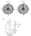
variable impedance device 25, by the single antenna 20 (the laminatedceramic chip antenna 211 does not act as an antenna), different radiation characteristics were obtained. - In the present example, as shown in Fig. 6, unlike Mounting Example 1, as the
coupling element 21, a micro-strip line antenna formed by a circuit pattern of the printedcircuit board 26 was used. Other aspects were identical to those of Mounting Example 1 and a measurement example thereof is as shown in Fig. 7(a) and Fig. 7(b). - As can be clearly understood in a comparison between Fig. 7 (a) and Fig. 7(b), only by turning on/off the switch, which corresponds to the
variable impedance device 25, by the single antenna 20 (themicro-strip line antenna 212 does not act as an antenna), different radiation characteristics were obtained. - In Mounting Examples 1 and 2, the
coupling element 21 whose specifications were known at the design phase was used. However, as shown in Fig. 8 and Fig. 9, acoupling element 21 whose specifications are unknown at the design phase may also be used. - In the example shown in Fig. 8, a
connection point 213 having conductivity is provided on the side of the printedcircuit board 26, and thevariable impedance device 25 is connected to thisconnection point 213. Then, when this wireless device is attached to an electronic apparatus such as a personal computer and used, thevariable impedance device 25 is connected to thiselectronic apparatus ground 102 via theconnection point 213. - Finally, the above results in a construction almost identical to
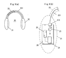
Embodiment 1, and by turning on/off thevariable impedance device 25, two types of radiation characteristics can be obtained in terms of thesingle antenna 20. - Furthermore, as shown in Fig. 9(a), the present invention can also be applied to a
headphone 30 having an inverseU-shaped belt portion 33 and twopad portions headphone 30 is provided with a metal wire frame 311, in general, inside thebelt portion 33 for reinforcement or other purposes. - Then, as shown in Fig. 9(b) in an enlarged manner, it is satisfactory to provide a member similar to the
connection point 213 on theprint circuit wire 26 and electrically connect thisconnection point 213 to thewire frame 331. - In addition to the above, various mounting examples can be considered, and even when a
coupling element 21 whose specifications are unknown in the design phase is used, effects of diversity can be obtained as long as some change in radiation characteristics of theantenna 20 is caused by turning on/off of thevariable impedance device 25. - Fig. 10 is a block diagram of a wireless device according to Embodiment 3 of the present invention. In the drawing, components identical to those of
Embodiment 2 are signified by identical symbols, whereby a description thereof will be omitted. - As shown in Fig. 11, in Embodiment 3, two surface-mounting
antennas circuit board 26, whereby theseantennas - In addition, the
antennas - As shown in Fig. 10, an antenna changeover signal S2 is outputted from the modulator/
demodulator circuit 245 to anantenna switch 41. Theantenna switch 41 alternatively selects an antenna for use for communications out of theseantennas - Herein, unlike
Embodiment 2, the selected antenna (including the antenna 40) is fed with electrical power from the feed line L, and thereby acts as an antenna. - In the present embodiment, even in the case where the mounting area of the antenna is narrow and effects of space diversity are hardly obtainable, effects of directional diversity can be provided.
- Furthermore, the surface-mounting antennas are arranged on one surface of the circuit board in a concentrated fashion, therefore, a thin wireless device can be constructed.
- In the foregoing descriptions of
Embodiments 2 and 3, examples where thewireless module 24 carries out both modulation and demodulation were described, however, the present invention can also be applied, as well, to a case where thewireless module 24 carries out only one of these. - Having described preferred embodiments of the invention with reference to the accompanying drawings, it is to be understood that the invention is not limited to those precise embodiments, and that various changes and modifications may be effected therein by one skilled in the art without departing from the scope or spirit of the invention as defined in the appended claims.
Claims (13)
- A card device(10) to be inserted into a slot(101) of an electronic apparatus(100) having an electronic apparatus ground(102) and electrically connected to this electronic apparatus(100), comprising:a carrier(11),a single antenna(12) provided on said carrier(11),a card ground(13) which is disposed in said carrier(11) and electrically connected to said antenna(12), anda switch(14) for carrying out, with a high frequency, a connection/disconnection of said card ground(13) to/from said electronic apparatus ground(102) in a condition where this card device(10) is inserted in said slot(101).
- A card device(10) as set forth in Claim 1 comprising:demodulating means(15) which accepts a signal received by said antenna(12) for demodulation,judging means(16) which accepts the signal demodulated by said demodulating means(15) and judges the quality of the communications state of said antenna(12), anda control means(17) for controlling said switch(14) with reference to the judgment result of said judging means(16).
- A card device(10) as set forth in Claim 1, wherein
said antenna(12) is a w1/4 chip antenna exposed outside said carrier(11). - An electronic apparatus(100) in which the card device(10) as set forth in Claim 1 is inserted in a slot(101) thereof.
- A wireless device comprising:an antenna(20) and a coupling element(21) which is electrically coupled to this antenna(20), whereinelectrical characteristics of said coupling element(21) are made variable, so that a plurality of radiation characteristics can be obtained by said antenna(20).
- A wireless device comprising:an antenna(20),a wireless module(24) which feeds electrical power to said antenna(20) andtransmits information via said antenna(20),a coupling element(21) which is arranged in contiguity with said antenna(20) and electrically coupled to said antenna(20), anda variable impedance device(25) provided between said coupling element(21) and a ground point, whereinsaid wireless module(24) operates said variable impedance device(25) to change the impedance between said coupling element(21) and ground point, so that a plurality of radiation characteristics are obtained by said antenna(20).
- A wireless device as set forth in Claim 6, wherein
said variable impedance device(25) varies impedance between two levels of high impedance and low impedance. - A wireless device as set forth in Claim 6, wherein
said coupling element(21) is an element for an antenna(211) to which no electrical power is supplied. - A wireless device as set forth in Claim 6, wherein
said coupling element(21) is a circuit pattern(212). - A wireless device as set forth in Claim 6, wherein
said coupling element(21) is a component of an electronic apparatus to which this wireless device is attached. - A wireless device as set forth in Claim 10, wherein
said component is a ground(102). - A wireless device as set forth in Claim 10, wherein
said component is a wire frame(331). - A wireless device comprising:a substrate(26),a plurality of antennas(20)(40) which are arranged in contiguity with each other on one surface of said substrate(26) and electrically coupled to each other,an antenna switch(41) for alternatively selecting an antenna for use for communications out of these antennas(20)(40), anda wireless module(24) which outputs an antenna changeover signal to the antenna switch(41), feeds electrical power to an antenna selected by said antenna switch(41), and transmits information via this antenna.
Applications Claiming Priority (2)
| Application Number | Priority Date | Filing Date | Title |
|---|---|---|---|
| JP2001220406 | 2001-07-19 | ||
| JP2001220406 | 2001-07-19 |
Publications (3)
| Publication Number | Publication Date |
|---|---|
| EP1278155A2 true EP1278155A2 (en) | 2003-01-22 |
| EP1278155A3 EP1278155A3 (en) | 2004-01-21 |
| EP1278155B1 EP1278155B1 (en) | 2006-09-06 |
Family
ID=19054226
Family Applications (1)
| Application Number | Title | Priority Date | Filing Date |
|---|---|---|---|
| EP02015168A Expired - Lifetime EP1278155B1 (en) | 2001-07-19 | 2002-07-08 | Card device comprising an antenna and connected with an electronic apparatus or a wireless device |
Country Status (3)
| Country | Link |
|---|---|
| US (1) | US7123938B2 (en) |
| EP (1) | EP1278155B1 (en) |
| DE (1) | DE60214484T2 (en) |
Cited By (1)
| Publication number | Priority date | Publication date | Assignee | Title |
|---|---|---|---|---|
| WO2008084273A2 (en) * | 2006-12-21 | 2008-07-17 | Nokia Corporation | An antenna device |
Families Citing this family (6)
| Publication number | Priority date | Publication date | Assignee | Title |
|---|---|---|---|---|
| KR100751938B1 (en) * | 2005-07-23 | 2007-08-24 | 엘지전자 주식회사 | Mobile handset platform including replaceable rf card, and data service system for using said replaceable rf card and method thereof |
| EP1777781B1 (en) * | 2005-10-19 | 2016-05-11 | KOFinder Technologies Inc. | Antenna arrangement |
| US8644853B2 (en) | 2008-05-12 | 2014-02-04 | Qualcomm Incorporated | Providing base station almanac to mobile station |
| US20100178934A1 (en) * | 2009-01-13 | 2010-07-15 | Qualcomm Incorporated | Environment-specific measurement weighting in wireless positioning |
| US8665156B2 (en) * | 2009-09-08 | 2014-03-04 | Qualcomm Incorporated | Position estimation assistance information for mobile station |
| US8437772B2 (en) * | 2009-09-15 | 2013-05-07 | Qualcomm Incorporated | Transmitter position integrity checking |
Citations (7)
| Publication number | Priority date | Publication date | Assignee | Title |
|---|---|---|---|---|
| US5557288A (en) * | 1994-09-07 | 1996-09-17 | International Business Machines Corporation | Antenna housing with extendable drawer for a portable computer |
| EP0735609A1 (en) * | 1995-03-31 | 1996-10-02 | Nokia Mobile Phones Ltd. | An antenna |
| EP0862278A2 (en) * | 1997-02-14 | 1998-09-02 | Nokia Mobile Phones Ltd. | A communication unit, an antenna and a method for connecting an antenna |
| WO1999054956A2 (en) * | 1998-04-20 | 1999-10-28 | Allgon Ab | Ground extension arrangement for coupling to ground means in an antenna system, and an antenna system and a mobile radio device having such ground arrangement |
| US6034638A (en) * | 1993-05-27 | 2000-03-07 | Griffith University | Antennas for use in portable communications devices |
| US6061025A (en) * | 1995-12-07 | 2000-05-09 | Atlantic Aerospace Electronics Corporation | Tunable microstrip patch antenna and control system therefor |
| WO2001031733A1 (en) * | 1999-10-29 | 2001-05-03 | Allgon Ab | Antenna device and method for transmitting and receiving radio waves |
Family Cites Families (18)
| Publication number | Priority date | Publication date | Assignee | Title |
|---|---|---|---|---|
| JPH05335826A (en) | 1991-11-18 | 1993-12-17 | Motorola Inc | Built-in antenna for communication equipment |
| JP3251680B2 (en) | 1991-12-26 | 2002-01-28 | 株式会社東芝 | Portable radio |
| GB9309368D0 (en) | 1993-05-06 | 1993-06-16 | Ncr Int Inc | Antenna apparatus |
| JPH07263941A (en) | 1994-03-23 | 1995-10-13 | Murata Mfg Co Ltd | Moving body communication machine |
| JPH08101900A (en) | 1994-09-30 | 1996-04-16 | Toshiba Corp | Ic card for radio communication and data processor mounted with the same |
| US6223990B1 (en) * | 1995-06-16 | 2001-05-01 | Rohm Co., Ltd. | Communication system including a dual passive antenna configuration |
| KR100213373B1 (en) | 1996-05-28 | 1999-08-02 | 이형도 | An antenna for wireless lan card |
| JPH1075192A (en) | 1996-08-30 | 1998-03-17 | Matsushita Electric Ind Co Ltd | Antenna device |
| JPH10214232A (en) * | 1997-01-30 | 1998-08-11 | Rohm Co Ltd | Ic card, and ic card operating method |
| JPH10240883A (en) * | 1997-02-24 | 1998-09-11 | Toshiba Corp | Ic card system, and security method therefor |
| JP3646472B2 (en) * | 1997-05-19 | 2005-05-11 | 株式会社日立製作所 | Non-contact type IC card and transmission / reception circuit |
| FI980300A (en) * | 1998-02-10 | 1999-08-11 | Nokia Mobile Phones Ltd | Card-like wireless communication means |
| JP2001119222A (en) | 1999-10-20 | 2001-04-27 | Matsushita Electric Ind Co Ltd | Small radio |
| JP4501241B2 (en) * | 2000-07-10 | 2010-07-14 | ソニー株式会社 | IC card and IC card data communication method |
| JP3676244B2 (en) * | 2001-02-02 | 2005-07-27 | 三菱電機株式会社 | Portable device terminal and peripheral device for acoustic test of portable device terminal |
| US20030051178A1 (en) * | 2001-09-12 | 2003-03-13 | Ping Liu | Mechanism for wireless modem power control |
| JP3763764B2 (en) * | 2001-09-18 | 2006-04-05 | シャープ株式会社 | Plate-like inverted F antenna and wireless communication device |
| US7057560B2 (en) * | 2003-05-07 | 2006-06-06 | Agere Systems Inc. | Dual-band antenna for a wireless local area network device |
-
2002
- 2002-07-08 EP EP02015168A patent/EP1278155B1/en not_active Expired - Lifetime
- 2002-07-08 DE DE60214484T patent/DE60214484T2/en not_active Expired - Fee Related
- 2002-07-17 US US10/198,619 patent/US7123938B2/en not_active Expired - Fee Related
Patent Citations (7)
| Publication number | Priority date | Publication date | Assignee | Title |
|---|---|---|---|---|
| US6034638A (en) * | 1993-05-27 | 2000-03-07 | Griffith University | Antennas for use in portable communications devices |
| US5557288A (en) * | 1994-09-07 | 1996-09-17 | International Business Machines Corporation | Antenna housing with extendable drawer for a portable computer |
| EP0735609A1 (en) * | 1995-03-31 | 1996-10-02 | Nokia Mobile Phones Ltd. | An antenna |
| US6061025A (en) * | 1995-12-07 | 2000-05-09 | Atlantic Aerospace Electronics Corporation | Tunable microstrip patch antenna and control system therefor |
| EP0862278A2 (en) * | 1997-02-14 | 1998-09-02 | Nokia Mobile Phones Ltd. | A communication unit, an antenna and a method for connecting an antenna |
| WO1999054956A2 (en) * | 1998-04-20 | 1999-10-28 | Allgon Ab | Ground extension arrangement for coupling to ground means in an antenna system, and an antenna system and a mobile radio device having such ground arrangement |
| WO2001031733A1 (en) * | 1999-10-29 | 2001-05-03 | Allgon Ab | Antenna device and method for transmitting and receiving radio waves |
Cited By (3)
| Publication number | Priority date | Publication date | Assignee | Title |
|---|---|---|---|---|
| WO2008084273A2 (en) * | 2006-12-21 | 2008-07-17 | Nokia Corporation | An antenna device |
| WO2008084273A3 (en) * | 2006-12-21 | 2008-12-04 | Nokia Corp | An antenna device |
| US8525734B2 (en) | 2006-12-21 | 2013-09-03 | Nokia Corporation | Antenna device |
Also Published As
| Publication number | Publication date |
|---|---|
| US20030017849A1 (en) | 2003-01-23 |
| EP1278155B1 (en) | 2006-09-06 |
| DE60214484D1 (en) | 2006-10-19 |
| DE60214484T2 (en) | 2007-09-20 |
| EP1278155A3 (en) | 2004-01-21 |
| US7123938B2 (en) | 2006-10-17 |
Similar Documents
| Publication | Publication Date | Title |
|---|---|---|
| US6781548B2 (en) | Electrically connected multi-feed antenna system | |
| US7605766B2 (en) | Multi-band antenna device for radio communication terminal and radio communication terminal comprising the multi-band antenna device | |
| CN102598410B (en) | Omnidirectional multi-band antennas | |
| US6700543B2 (en) | Antenna element with conductors formed on outer surfaces of device substrate | |
| US20040113848A1 (en) | Integrated tri-band antenna for laptop applications | |
| EP1079463A2 (en) | Asymetric dipole antenna assembly | |
| JP2005525036A (en) | Antenna device and module including antenna device | |
| KR20060094716A (en) | Antenna module and electric apparatus using the same | |
| EP1231671B1 (en) | Internal antenna for mobile communications device | |
| WO2011163139A1 (en) | Wideband printed circuit board-printed antenna for radio frequency front end circuit | |
| US6437745B1 (en) | Expansion card for wireless data transmission and antenna structure for the same | |
| EP1717901B1 (en) | Built-in type antenna apparatus for portable terminal | |
| US20070139271A1 (en) | Method for access to a medium by a multi-channel device | |
| EP1278155A2 (en) | Card device comprising an antenna and connected with an electronic apparatus or a wireless device | |
| US20020123312A1 (en) | Antenna systems including internal planar inverted-F Antenna coupled with external radiating element and wireless communicators incorporating same | |
| US7205943B2 (en) | Printed antenna | |
| US6850738B2 (en) | Method and antenna arrangement for coupling external antennas to a communication unit | |
| JP3383046B2 (en) | Wireless device | |
| US6914568B2 (en) | Integral antenna and radio system | |
| CN114914666B (en) | Antenna and electronic equipment | |
| JP3947812B2 (en) | Card device, electronic device and wireless device | |
| US20030080903A1 (en) | Printed conductive mesh dipole antenna and method | |
| JP6426564B2 (en) | Card type electronic device | |
| JP3113460B2 (en) | Mobile communication device | |
| CN117117458A (en) | Electronic equipment |
Legal Events
| Date | Code | Title | Description |
|---|---|---|---|
| PUAI | Public reference made under article 153(3) epc to a published international application that has entered the european phase |
Free format text: ORIGINAL CODE: 0009012 |
|
| AK | Designated contracting states |
Kind code of ref document: A2 Designated state(s): AT BE BG CH CY CZ DE DK EE ES FI FR GB GR IE IT LI LU MC NL PT SE SK TR |
|
| AX | Request for extension of the european patent |
Free format text: AL;LT;LV;MK;RO;SI |
|
| PUAL | Search report despatched |
Free format text: ORIGINAL CODE: 0009013 |
|
| AK | Designated contracting states |
Kind code of ref document: A3 Designated state(s): AT BE BG CH CY CZ DE DK EE ES FI FR GB GR IE IT LI LU MC NL PT SE SK TR |
|
| AX | Request for extension of the european patent |
Extension state: AL LT LV MK RO SI |
|
| RIC1 | Information provided on ipc code assigned before grant |
Ipc: 7H 01Q 1/24 B Ipc: 7G 06K 19/07 A |
|
| 17P | Request for examination filed |
Effective date: 20040419 |
|
| 17Q | First examination report despatched |
Effective date: 20040607 |
|
| AKX | Designation fees paid |
Designated state(s): DE FR GB |
|
| GRAP | Despatch of communication of intention to grant a patent |
Free format text: ORIGINAL CODE: EPIDOSNIGR1 |
|
| GRAS | Grant fee paid |
Free format text: ORIGINAL CODE: EPIDOSNIGR3 |
|
| GRAA | (expected) grant |
Free format text: ORIGINAL CODE: 0009210 |
|
| AK | Designated contracting states |
Kind code of ref document: B1 Designated state(s): DE FR GB |
|
| REG | Reference to a national code |
Ref country code: GB Ref legal event code: FG4D |
|
| REF | Corresponds to: |
Ref document number: 60214484 Country of ref document: DE Date of ref document: 20061019 Kind code of ref document: P |
|
| ET | Fr: translation filed | ||
| PLBE | No opposition filed within time limit |
Free format text: ORIGINAL CODE: 0009261 |
|
| STAA | Information on the status of an ep patent application or granted ep patent |
Free format text: STATUS: NO OPPOSITION FILED WITHIN TIME LIMIT |
|
| 26N | No opposition filed |
Effective date: 20070607 |
|
| PGFP | Annual fee paid to national office [announced via postgrant information from national office to epo] |
Ref country code: FR Payment date: 20090710 Year of fee payment: 8 |
|
| PGFP | Annual fee paid to national office [announced via postgrant information from national office to epo] |
Ref country code: DE Payment date: 20090702 Year of fee payment: 8 Ref country code: GB Payment date: 20090708 Year of fee payment: 8 |
|
| GBPC | Gb: european patent ceased through non-payment of renewal fee |
Effective date: 20100708 |
|
| REG | Reference to a national code |
Ref country code: FR Ref legal event code: ST Effective date: 20110331 |
|
| PG25 | Lapsed in a contracting state [announced via postgrant information from national office to epo] |
Ref country code: DE Free format text: LAPSE BECAUSE OF NON-PAYMENT OF DUE FEES Effective date: 20110201 |
|
| REG | Reference to a national code |
Ref country code: DE Ref legal event code: R119 Ref document number: 60214484 Country of ref document: DE Effective date: 20110201 |
|
| PG25 | Lapsed in a contracting state [announced via postgrant information from national office to epo] |
Ref country code: FR Free format text: LAPSE BECAUSE OF NON-PAYMENT OF DUE FEES Effective date: 20100802 |
|
| PG25 | Lapsed in a contracting state [announced via postgrant information from national office to epo] |
Ref country code: GB Free format text: LAPSE BECAUSE OF NON-PAYMENT OF DUE FEES Effective date: 20100708 |