EP1277286B1 - Personal communications device with gps receiver and comon clock source - Google Patents
Personal communications device with gps receiver and comon clock source Download PDFInfo
- Publication number
- EP1277286B1 EP1277286B1 EP01924707A EP01924707A EP1277286B1 EP 1277286 B1 EP1277286 B1 EP 1277286B1 EP 01924707 A EP01924707 A EP 01924707A EP 01924707 A EP01924707 A EP 01924707A EP 1277286 B1 EP1277286 B1 EP 1277286B1
- Authority
- EP
- European Patent Office
- Prior art keywords
- signal
- frequency
- output
- controlled oscillator
- phase
- Prior art date
- Legal status (The legal status is an assumption and is not a legal conclusion. Google has not performed a legal analysis and makes no representation as to the accuracy of the status listed.)
- Expired - Lifetime
Links
Images


Classifications
-
- H—ELECTRICITY
- H03—ELECTRONIC CIRCUITRY
- H03L—AUTOMATIC CONTROL, STARTING, SYNCHRONISATION, OR STABILISATION OF GENERATORS OF ELECTRONIC OSCILLATIONS OR PULSES
- H03L7/00—Automatic control of frequency or phase; Synchronisation
- H03L7/06—Automatic control of frequency or phase; Synchronisation using a reference signal applied to a frequency- or phase-locked loop
- H03L7/08—Details of the phase-locked loop
- H03L7/081—Details of the phase-locked loop provided with an additional controlled phase shifter
-
- G—PHYSICS
- G01—MEASURING; TESTING
- G01S—RADIO DIRECTION-FINDING; RADIO NAVIGATION; DETERMINING DISTANCE OR VELOCITY BY USE OF RADIO WAVES; LOCATING OR PRESENCE-DETECTING BY USE OF THE REFLECTION OR RERADIATION OF RADIO WAVES; ANALOGOUS ARRANGEMENTS USING OTHER WAVES
- G01S19/00—Satellite radio beacon positioning systems; Determining position, velocity or attitude using signals transmitted by such systems
- G01S19/01—Satellite radio beacon positioning systems transmitting time-stamped messages, e.g. GPS [Global Positioning System], GLONASS [Global Orbiting Navigation Satellite System] or GALILEO
- G01S19/13—Receivers
- G01S19/23—Testing, monitoring, correcting or calibrating of receiver elements
- G01S19/235—Calibration of receiver components
-
- H—ELECTRICITY
- H03—ELECTRONIC CIRCUITRY
- H03L—AUTOMATIC CONTROL, STARTING, SYNCHRONISATION, OR STABILISATION OF GENERATORS OF ELECTRONIC OSCILLATIONS OR PULSES
- H03L7/00—Automatic control of frequency or phase; Synchronisation
- H03L7/06—Automatic control of frequency or phase; Synchronisation using a reference signal applied to a frequency- or phase-locked loop
- H03L7/16—Indirect frequency synthesis, i.e. generating a desired one of a number of predetermined frequencies using a frequency- or phase-locked loop
- H03L7/18—Indirect frequency synthesis, i.e. generating a desired one of a number of predetermined frequencies using a frequency- or phase-locked loop using a frequency divider or counter in the loop
- H03L7/197—Indirect frequency synthesis, i.e. generating a desired one of a number of predetermined frequencies using a frequency- or phase-locked loop using a frequency divider or counter in the loop a time difference being used for locking the loop, the counter counting between numbers which are variable in time or the frequency divider dividing by a factor variable in time, e.g. for obtaining fractional frequency division
- H03L7/1974—Indirect frequency synthesis, i.e. generating a desired one of a number of predetermined frequencies using a frequency- or phase-locked loop using a frequency divider or counter in the loop a time difference being used for locking the loop, the counter counting between numbers which are variable in time or the frequency divider dividing by a factor variable in time, e.g. for obtaining fractional frequency division for fractional frequency division
- H03L7/1976—Indirect frequency synthesis, i.e. generating a desired one of a number of predetermined frequencies using a frequency- or phase-locked loop using a frequency divider or counter in the loop a time difference being used for locking the loop, the counter counting between numbers which are variable in time or the frequency divider dividing by a factor variable in time, e.g. for obtaining fractional frequency division for fractional frequency division using a phase accumulator for controlling the counter or frequency divider
Definitions
- This invention is generally related to a personal communications device having global positioning system receiver provisions which are clocked via a clock signal derived from a clock source shared with CDMA based radio. More particularly, the invention provides for a fractional N-synthesizer for providing a feedback signal for controlling an oscillator signal output frequency.
- GPS global positioning
- circuitry and components necessary to provide the global positioning capabilities must share the same enclosure and circuit board real estate as the circuitry and components dedicated to providing, for example, mobile (cellular) telephone capabilities.
- circuitry and components for both GPS capabilities as well as mobile telephone capabilities are powered by the same power source, typically, via an on-board battery. While battery technology is improving, it is typical that the more power consumed by a device the larger the physical size of the battery necessary to provide a given operating time.
- GPS receiver 100 includes an associated oscillator 101 while CDMA device 200 includes an associated oscillator 201.
- oscillator 101 and 201 provides a clock signal to the respective circuitry to which it is associated.
- FIG.2 shows a GPS receiver 100, which includes an oscillator 101.
- Oscillator 101 provides a signal of a particular frequency to phase comparator 146.
- Phase comparator 146 also receives input from frequency divider 136 and outputs a signal to loop filter 145.
- Loop filter 145 provides a signal to voltage controlled oscillator (VCO) 115 which generates an output signal whose frequency is contingent upon the signal input from loop filter 145.
- the signal from VCO 115 is provided to mixer 110 where it is combined with a radio frequency (RF) signal from low noise amplifier (LNA) 105 to produce a first intermediate frequency (IF) signal S1.
- RF radio frequency
- LNA low noise amplifier
- the signal S1 is combined with a signal S2 from frequency divider 130 to produce an in-phase second IF frequency output signal S3.
- the signal S1 is combined with a signal S4 from frequency divider 130 to produce a quadrature-phase second IF frequency output signal S5.
- Signal S3 is provided to comparator and A to D processor 125 to produce a digitized signal I for output to GPS baseband section 150.
- Signal S5 is provided to comparator and A to D processor 126 to produce a digitized signal Q for output to GPS baseband section 150.
- Frequency divider 130 also provides its output signal S4 to frequency divider 135 and frequency divider 136.
- the output from VCO 115 is also provided to frequency divider 130.
- Frequency divider 130 outputs a signal S5 that is mixed by mixer 121 with a signal S1 to produce a signal S4.
- GPS global positioning systems
- the invention seeks to provide a personal communications device 10 having global positioning system (GPS) capabilities.
- the invention seeks to provide a personal communications device 10 in which a single oscillator 201 acts as a clock source for both mobile telephone circuitry 200 and global positioning system (GPS) circuitry 100.
- GPS circuitry 100 includes fractional synthesizer provisions for controlling the generation of the frequency of signals based upon the oscillator 201.
- FIG. 3 shows a block diagram of a personal communications device 10 according to the invention.
- GPS global positioning system
- CDMA code division multiple access
- GPS receiver 100 includes a GPS radio 102 and a GPS baseband unit 103.
- GPS radio 102 receives and processes GPS signals and provides them to the baseband unit 103 for further extraction of data from a received GPS signal.
- CDMA radio unit 202 for receiving, processing and transmitting CDMA based RF signals and a CDMA baseband unit 203 for further processing of CDMA RF signals received or to be transmitted.
- CDMA telecommunications unit 200 includes an oscillator 201 for providing a clock signal to circuitry of COMA telecommunications unit 200 and to GPS receiver 100. More particularly CDMA oscillator 201 provides a clock signal to CDMA radio 202, CDMA baseband unit 203 and to GPS receiver 102 and GPS baseband unit 103.
- FIG. 4 shows a diagram detailing GPS receiver 100.
- a voltage controlled oscillator (VCO) 115 which generates a GPS system clock signal Z whose frequency is contingent upon the voltage input from loop filter 145.
- the output from VCO 115 is provided to mixer 110 where it is combined with a received radio frequency (RF) input signal from low noise amplifier (INA) 105 to produce a first intermediate frequency (IF) signal S1.
- RF radio frequency
- INA low noise amplifier
- IF intermediate frequency
- This first IF signal S1 is provided to amplifier 112 and then to mixer 120 and mixer 121.
- mixer 120 it is combined with a signal S2 from frequency divider 130 to produce a second IF frequency output signal S3.
- second IF frequency output signal S1 is combined with a signal S4 also from frequency divider 130 to produce a further IF frequency output signal S5.
- Signal S4 is also provided to frequency divider 135 where it is converted into a signal of alternate frequency S6 and output to GPS baseband unit 150.
- Signal S3 is input to comparator and A to D processor 125 where it is processed and converted into a digital output signal I for input to GPS baseband unit 150.
- signal S5 is input to comparator and A to D processor 126 where it is processed and converted into digital output signal Q which is provided to GPS baseband unit 150.
- the GPS system clock signal Z output from VCO 115 is also provided to frequency divider 130 and a frequency synthesizer 116.
- Frequency divider 116 converts the signal Z from VCO 115 into a feedback signal S7 that is provided to phase comparator 146 which outputs a control signal S9 to loop filter 145 in response to the input of the feedback signal S7 and the clock signal S8 from oscillator 201.
- Control signal S9 is then provided to VCO 115, which adjusts the frequency of output signal Z in accordance with the control signal S9.
- FIG. 5 is a block diagram of the phase interpolated fractional N frequency synthesizer 116.
- the synthesizer 116 can be implemented as an integrated circuit using known CMOS fabrication methods or other compatible semiconductor chip technologies.
- a reference signal Z from VCO 115 is provided to an input of a phase detector 322.
- the output of the phase-detector 322 is provided to a loop filter 324.
- the output of the loop filter 324 is provided to a controlled oscillator 326, such as a VCO, which has an output S7 (feedback signal S7) that is the output of the synthesizer 116.
- the signal S7 is supplied to a fractional-N divider 328.
- a control word K is supplied to the fractional-N divider 328 in order to set the value of the divisor N.
- the output of the fractional-N divider 328 is provided to a phase compensation circuit 330 and to an on chip tuning circuit 332, which in combination are referred to as a phase compensator.
- the output (fcomp) from the phase compensation circuit 330 is provided as the second input to the phase detector 322.
- An accumulator 334 also receives control word K and the signal Z.
- the carry out port (the carry signal S10) from the accumulator 334 also serves as an input to the fractional-N divider 328.
- the signal Z serves as the clocking signal for the accumulator 334.
- the signal S10 from carry out port of the accumulator 334 triggers the divide by the N+1 function of the fractional-N divider.
- phase detector 322, loops filter 324 and VCO 326 may be of any suitable type known to those of ordinary skill.
- the types of phase detectors, loop filters, VCOs and fractional-N dividers commonly used in fractional-N synthesizers can be used for the synthesizer 320, such as voltage or current controlled oscillators, phase or phase/frequency detectors, active or passive loop filters and loop filters with charge pumps.
- FIG. 6 shows a more detailed description of an embodiment of phase compensation circuit 330 and on-chip tuning circuit 332.
- Phase compensation circuit 330 and on-chip tuning circuit 332 may be implemented using an arrangement of voltage controlled delay elements (D) where the amount of delay elements D provides a signal delay of Tvco/4, where Tvco equals the period of the frequency of the output S10 of the VCO 326.
- D voltage controlled delay elements
- the output of the fractional-N divider 328 is applied to the series of delay lines whose outputs are identified as ⁇ 1- ⁇ 4. It will be noted that ⁇ 1 has no delay elements, while ⁇ 2 has a single delay element, ⁇ 3 has two delay elements and ⁇ 4 has three delay elements.
- the signals ⁇ 1- ⁇ 4 are provided to control circuitry 339 that has an output signal fcomp that is applied to an input of the phase detector 322 as shown in FIG. 5.
- the output fcomp of control circuitry 339 is selectively switched among the inputs ⁇ 1- ⁇ 4 according to the output of the accumulator 334 which is provided to the control circuit 339.
- the on-chip tuning circuit 332 includes four voltage control delay elements D, a phase detector 336 and a loop filter 338.
- the on-chip tuning circuit 332 is implemented as a delay locked loop.
- the signal S10 from VCO 326 passes through the four delay elements (D) of the on-chip tuning circuit 332 and is then provided to the phase detector 336.
- S10 is also applied to the phase detector 336.
- the phase detector 336 outputs a signal proportional to the difference in phased between the two input signals.
- the output of the phase detector 336 then passes through a loop filter 338.
- the output Vc of the loop filter 338 is used as a control voltage for each of the delay elements D of the on-chip tuning circuit 332.
- Control voltage Vc is also applied to each delay element (D) of the tuning circuit 332 is 1 ⁇ 4 the period of the frequency of the input signal to the delay locked loop.
- the tuning circuit 332 determines or adjusts the value of the delay elements according to the input frequency.
- the accumulator 334 is programmed (via control word K) to generate a carry signal at every fourth cycle of the signal Z.
- Each time interval T is equal to one cycle of Z.
- T1-T4 S10 has 17 cycles and Z has 4 cycles.
- the fractional-N divider 328 divides the signal S10 by 4.
- the divider 328 again divides the signal S10 by 4.
- the phase compensation circuit 330 provides the signal ⁇ 1 to the phase detector 322.
- signal ⁇ 1 is in phase with the signal Z.
- the output of the phase compensation circuit 330 switches to ⁇ 2.
- Switching of the output of the control circuit 339 is controlled by the output of the accumulator 334, which is clocked by the signal Z. It will be noted that ⁇ 2 is in phase with Z at the output of the phase compensation circuit 330.
- the output of the phase compensation circuit 330 switches to ⁇ 3 and then at the beginning of the time period T4, the output of the phase compensation circuit 330 switches to ⁇ 4.
- the pattern then repeats. In this way, compensation for the phase lag of the divider 328 is accomplished.
- FIG. 8 illustrates an alternate embodiment in which provisions are made for selectively providing feedback to phase comparator 146 via fractional N synthesizer 116 or a frequency divider 136.
- a switch 250 is provided for switching between the output of fractional N synthesizer 116 or frequency divider 136 for input to phase comparator 146.
- Switch 250 may be a multiplexor or other logic gating. Further, switch 250 can be permanently set to a desired position during manufacturer or could remain selectively switchable and controllable via application of an appropriate switching signal.
- the present invention can be implemented in the systems described in U.S. in U.S. Patent No. 5.874.914 for "GPS Receiver Utilizing A Communication Link” and in U.S. Patent No. 5.841,396 also, for a "GPS Receiver Utilizing A Communication Link".
- GPS global positioning system
- a local oscillator is coupled to the downconverter and provides a reference signal to the downconverter to convert the GPS signals from a first frequency to a second frequency.
- a second antenna is provided for receiving a precision carrier frequency signal from a source of the precision carrier frequency signal.
- An automatic frequency control (AFC) circuit is coupled to the second antenna.
- the AFC circuit provides a second reference signal to the local oscillator to calibrate the first reference signal from the local oscillator.
- the local oscillator is used to acquire the GPS signals.
- GPS receiver having a first antenna for receiving GPS signals and a downconverter coupled to the first antenna.
- the first antenna provides the GPS signals to the downconverter.
- the downconverter has an input for receiving a local oscillator signal to convert the GPS signals from a first frequency to a second frequency.
- the second antenna is provided for receiving a precision carrier frequency signal from a source providing the precision carrier frequency signal.
- An automatic frequency control (AFC) circuit is coupled to the second antenna.
- the AFC circuit is also coupled to the downconverter to provide the local oscillator signal that is used to acquire the GPS signals.
- U.S. Patent No. 6.002.363 discloses among other things a GPS receiver which includes a GPS antenna for receiving data representative of GPS signals from at least one satellite: a digital processor coupled to the GPS antenna, the digital processor processes the data representative of GPS signals from at least one satellite, including performing a matched filtering operation to determine a pseudorange based on the data representative of GPS signals. The digital processor also processes communication signals received through a communication link, the processing of communication signals comprising demodulation of communication signals sent to the GPS receiver.
- U.S. Patent No. 5,734,966 discloses among other things a frequency tolerant wireless transceiver to receive and transmit on the wireless signal energy on the same frequency and to automatically adjust to that frequency, the transceiver includes: an antenna to receive a wireless data signal, including application data from one or more remote transceivers, at an actual frequency and issue this signal as a conducted radio frequency (RF) data signal and to transmit a wireless return signal at the actual frequency to the remote transceiver in response to a conducted RF return signal: a synthesizer to generate a local oscillator (LO) signal sequentially in response to a first and a second frequency control signal, and to generate the RF return signal at the actual frequency in response to the second frequency control signal and having modulation in response to a digital return signal; a direct conversion receiver to receive the LO signal to down convert the LO signal to down convert the LO signal.
- LO local oscillator
- a frequency tolerant transceiver to automatically adjust to receive a radio frequency (RF) data signal on an actual frequency and to transmit an RF return signal on that same frequency
- the transceiver comprising: a synthesizer for sequentially generating a local oscillator (LO) signal and the RF return signal, the LO signal sequentially having a first frequency corresponding to an expected frequency of the RF data signal and a second frequency corresponding to the actual frequency of the RF data signal in response to a first and a second frequency control signal, respectively, the RF return signal having the second frequency in response to the second frequency control signal; and a microcontroller system having a receive adjust mode for providing the first frequency control signal predictive of the expected frequency and providing the second frequency control signal for the actual frequency based upon a frequency difference between the actual frequency and the expected frequency.
- LO local oscillator
- the personal communications device of the invention can be implemented in hardware, software, firmware, or a combination thereof.
- the personal communications device is implemented in software or firmware that is stored in a memory and that is executed by a suitable instruction execution system.
- the personal communications device of the invention can implemented with any or a combination of the following technologies, which are all well known in the art: a discrete logic circuit(s) having logic gates for implementing logic functions upon data signals, an application specific integrated circuit having appropriate logic gates, a programmable gate array(s) (PGA), a fully programmable gate array (FPGA), etc.
Landscapes
- Engineering & Computer Science (AREA)
- Radar, Positioning & Navigation (AREA)
- Remote Sensing (AREA)
- Computer Networks & Wireless Communication (AREA)
- Physics & Mathematics (AREA)
- General Physics & Mathematics (AREA)
- Position Fixing By Use Of Radio Waves (AREA)
- Stabilization Of Oscillater, Synchronisation, Frequency Synthesizers (AREA)
- Circuits Of Receivers In General (AREA)
- Electric Clocks (AREA)
- Superheterodyne Receivers (AREA)
- Mobile Radio Communication Systems (AREA)
Abstract
Description
- This invention is generally related to a personal communications device having global positioning system receiver provisions which are clocked via a clock signal derived from a clock source shared with CDMA based radio. More particularly, the invention provides for a fractional N-synthesizer for providing a feedback signal for controlling an oscillator signal output frequency.
- Personal communications devices incorporating global positioning (GPS) capabilities are becoming popular. In these devices, the circuitry and components necessary to provide the global positioning capabilities must share the same enclosure and circuit board real estate as the circuitry and components dedicated to providing, for example, mobile (cellular) telephone capabilities. Further, circuitry and components for both GPS capabilities as well as mobile telephone capabilities are powered by the same power source, typically, via an on-board battery. While battery technology is improving, it is typical that the more power consumed by a device the larger the physical size of the battery necessary to provide a given operating time.
- The demand for smaller, more compact personal communication devices is increasing. Concurrent with this increasing demand for compactness is the demand for devices that provide for increased functionality and capabilities. As functionality and capabilities increase, typically, so does the need for power and printed circuit real estate within the personal communications device.
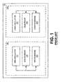
- In personal communications devices such as that shown in the block diagram of FIG. 1, wherein there is provided a personal communications device that incorporates a global positioning systems (GPS)
receiver 100 and a code division multiple access (CDMA) basedtelecommunications device 200, it is common for separate clock sources (oscillators) to be associated with theGPS receiver 100 and theCDMA device 200. More particularly,GPS receiver 100 includes an associatedoscillator 101 whileCDMA device 200 includes an associatedoscillator 201. Each oscillator, 101 and 201 provides a clock signal to the respective circuitry to which it is associated. - FIG.2 shows a
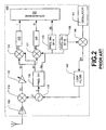
GPS receiver 100, which includes anoscillator 101.Oscillator 101 provides a signal of a particular frequency tophase comparator 146.Phase comparator 146 also receives input fromfrequency divider 136 and outputs a signal to loopfilter 145.Loop filter 145 provides a signal to voltage controlled oscillator (VCO) 115 which generates an output signal whose frequency is contingent upon the signal input fromloop filter 145. The signal fromVCO 115 is provided tomixer 110 where it is combined with a radio frequency (RF) signal from low noise amplifier (LNA) 105 to produce a first intermediate frequency (IF) signal S1. This first IF signal S1 is provided tovariable amplifier 112 and then on to mixer 120 andmixer 121. Inmixer 120, the signal S1 is combined with a signal S2 fromfrequency divider 130 to produce an in-phase second IF frequency output signal S3. Inmixer 121, the signal S1 is combined with a signal S4 fromfrequency divider 130 to produce a quadrature-phase second IF frequency output signal S5. Signal S3 is provided to comparator and A toD processor 125 to produce a digitized signal I for output toGPS baseband section 150. Signal S5 is provided to comparator and A toD processor 126 to produce a digitized signal Q for output toGPS baseband section 150.Frequency divider 130 also provides its output signal S4 tofrequency divider 135 andfrequency divider 136. The output from VCO 115 is also provided tofrequency divider 130.Frequency divider 130 outputs a signal S5 that is mixed bymixer 121 with a signal S1 to produce a signal S4. - As two separate oscillators are provided within the same
personal communications device 10, printed and/or integrated circuit real estate is devoted to accommodating each oscillator and power consumption of two oscillators is greater than for one oscillator. Thus, an unaddressed need exists in the industry to address the previous mentioned deficiencies and inadequacies. - It is an object of the invention to provide an improved personal telecommunications device having both global positioning systems (GPS) and telecommunications provisions that share a common clock source.
- This object is achieved by a device and a method according to
claims - Further developments of the invention are given in the dependent claims.
- Other systems, methods, features, and advantages of the invention will be or become apparent to one with skill in the art upon examination of the following figures and detailed description.
- The invention can be better understood with reference to the following figures. The components in the figures are not necessarily to scale, emphasis instead being placed upon clearly illustrating the principles of the invention. In the figures, like reference numerals designate corresponding parts throughout the different views.
- FIG. 1 is a block diagram of a typical personal communications device;
- FIG. 2 is a schematic diagram of a GPS receiver;
- FIG. 3 is a block diagram of the invention;
- FIG. 4 is a schematic diagram of a personal communications device according to the invention;
- FIG. 5 is a schematic diagram of a Fractional-N synthesizer;
- FIG. 6 is a detailed description of an embodiment of a phase compensation circuit and an on-chip tuning circuit;
- FIG. FIG. 7 is a timing diagram illustrating the relationship between signals of the frequency synthesizer in relation to the signals of the compensation circuit; and
- FIG. 8 is a diagram showing a further embodiment of the invention.
- The invention seeks to provide a
personal communications device 10 having global positioning system (GPS) capabilities. The invention seeks to provide apersonal communications device 10 in which asingle oscillator 201 acts as a clock source for bothmobile telephone circuitry 200 and global positioning system (GPS)circuitry 100.GPS circuitry 100 includes fractional synthesizer provisions for controlling the generation of the frequency of signals based upon theoscillator 201. - FIG. 3 shows a block diagram of a
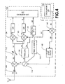
personal communications device 10 according to the invention. There is provided a global positioning system (GPS)receiver 100 and a code division multiple access (CDMA) basedtelecommunications unit 200.GPS receiver 100 includes aGPS radio 102 and aGPS baseband unit 103.GPS radio 102 receives and processes GPS signals and provides them to thebaseband unit 103 for further extraction of data from a received GPS signal. There is also provided aCDMA radio unit 202 for receiving, processing and transmitting CDMA based RF signals and aCDMA baseband unit 203 for further processing of CDMA RF signals received or to be transmitted.CDMA telecommunications unit 200 includes anoscillator 201 for providing a clock signal to circuitry ofCOMA telecommunications unit 200 and toGPS receiver 100. More particularlyCDMA oscillator 201 provides a clock signal toCDMA radio 202,CDMA baseband unit 203 and toGPS receiver 102 andGPS baseband unit 103. - FIG. 4 shows a diagram detailing
GPS receiver 100. There is provided a voltage controlled oscillator (VCO) 115 which generates a GPS system clock signal Z whose frequency is contingent upon the voltage input fromloop filter 145. The output from VCO 115 is provided tomixer 110 where it is combined with a received radio frequency (RF) input signal from low noise amplifier (INA) 105 to produce a first intermediate frequency (IF) signal S1. This first IF signal S1 is provided to amplifier 112 and then to mixer 120 andmixer 121. Atmixer 120 it is combined with a signal S2 fromfrequency divider 130 to produce a second IF frequency output signal S3. Atmixer 121 second IF frequency output signal S1 is combined with a signal S4 also fromfrequency divider 130 to produce a further IF frequency output signal S5. Signal S4 is also provided tofrequency divider 135 where it is converted into a signal of alternate frequency S6 and output toGPS baseband unit 150. - Signal S3 is input to comparator and A to
D processor 125 where it is processed and converted into a digital output signal I for input toGPS baseband unit 150. Likewise signal S5 is input to comparator and A toD processor 126 where it is processed and converted into digital output signal Q which is provided toGPS baseband unit 150. - The GPS system clock signal Z output from VCO 115 is also provided to
frequency divider 130 and afrequency synthesizer 116.Frequency divider 116 converts the signal Z from VCO 115 into a feedback signal S7 that is provided tophase comparator 146 which outputs a control signal S9 to loopfilter 145 in response to the input of the feedback signal S7 and the clock signal S8 fromoscillator 201. Control signal S9 is then provided to VCO 115, which adjusts the frequency of output signal Z in accordance with the control signal S9. In this illustration it can be seen that there is formed a feedback loop composed offrequency synthesizer 116,phase comparator 146 andloop filter 145. - FIG. 5 is a block diagram of the phase interpolated fractional
N frequency synthesizer 116. Thesynthesizer 116 can be implemented as an integrated circuit using known CMOS fabrication methods or other compatible semiconductor chip technologies. In FIG. 5, a reference signal Z fromVCO 115 is provided to an input of aphase detector 322. The output of the phase-detector 322 is provided to aloop filter 324. The output of theloop filter 324 is provided to a controlledoscillator 326, such as a VCO, which has an output S7 (feedback signal S7) that is the output of thesynthesizer 116. The signal S7 is supplied to a fractional-N divider 328. A control word K is supplied to the fractional-N divider 328 in order to set the value of the divisor N. - The output of the fractional-
N divider 328 is provided to aphase compensation circuit 330 and to an onchip tuning circuit 332, which in combination are referred to as a phase compensator. The output (fcomp) from thephase compensation circuit 330 is provided as the second input to thephase detector 322. Anaccumulator 334 also receives control word K and the signal Z. The carry out port (the carry signal S10) from theaccumulator 334 also serves as an input to the fractional-N divider 328. The signal Z serves as the clocking signal for theaccumulator 334. The signal S10 from carry out port of theaccumulator 334 triggers the divide by the N+1 function of the fractional-N divider. - The
phase detector 322, loops filter 324 andVCO 326 may be of any suitable type known to those of ordinary skill. The types of phase detectors, loop filters, VCOs and fractional-N dividers commonly used in fractional-N synthesizers can be used for the synthesizer 320, such as voltage or current controlled oscillators, phase or phase/frequency detectors, active or passive loop filters and loop filters with charge pumps. - FIG. 6 shows a more detailed description of an embodiment of
phase compensation circuit 330 and on-chip tuning circuit 332.Phase compensation circuit 330 and on-chip tuning circuit 332 may be implemented using an arrangement of voltage controlled delay elements (D) where the amount of delay elements D provides a signal delay of Tvco/4, where Tvco equals the period of the frequency of the output S10 of theVCO 326. - The output of the fractional-
N divider 328 is applied to the series of delay lines whose outputs are identified as φ1-φ4. It will be noted that φ1 has no delay elements, while φ2 has a single delay element, φ3 has two delay elements and φ4 has three delay elements. The signals φ1-φ4 are provided to controlcircuitry 339 that has an output signal fcomp that is applied to an input of thephase detector 322 as shown in FIG. 5. The output fcomp ofcontrol circuitry 339 is selectively switched among the inputs φ1-φ4 according to the output of theaccumulator 334 which is provided to thecontrol circuit 339. - The on-
chip tuning circuit 332 includes four voltage control delay elements D, aphase detector 336 and aloop filter 338. In the on-chip tuning circuit 332 is implemented as a delay locked loop. The signal S10 fromVCO 326 passes through the four delay elements (D) of the on-chip tuning circuit 332 and is then provided to thephase detector 336. In addition S10 is also applied to thephase detector 336. Thephase detector 336 outputs a signal proportional to the difference in phased between the two input signals. The output of thephase detector 336 then passes through aloop filter 338. The output Vc of theloop filter 338 is used as a control voltage for each of the delay elements D of the on-chip tuning circuit 332. Control voltage Vc is also applied to each delay element (D) of thetuning circuit 332 is ¼ the period of the frequency of the input signal to the delay locked loop. Thetuning circuit 332 determines or adjusts the value of the delay elements according to the input frequency. - FIG. 7 illustrates a timing diagram which illustrates the relationship between various signals of the
synthesizer 116 in relation to the signals of thecompensation circuit 330 and on-chip tuning circuit 332. More particularly, FIG. 6b illustrates an example wherein S10 =4.25(Z). In this example, thedivider 328 is programmed for N=4 (via control word K). Theaccumulator 334 is programmed (via control word K) to generate a carry signal at every fourth cycle of the signal Z. Each time interval T is equal to one cycle of Z. During the time interval T1-T4, S10 has 17 cycles and Z has 4 cycles. During the time interval T1, the fractional-N divider 328 divides the signal S10 by 4. In the second time period T2 and the third time period T3, thedivider 328 again divides the signal S10 by 4. At the beginning of the fourth time period, T4, theaccumulator 334 generates the carry signal which causes the divider to divide by N+1, in this example N+1=5. Therefore, signal Z is divided by five during T4. - During the time period T1, the
phase compensation circuit 330, more specifically,control circuit 339, provides the signal φ1 to thephase detector 322. At the beginning of the time period T1, signal φ1 is in phase with the signal Z. At the beginning of the time period φ2, the output of thephase compensation circuit 330 switches to φ2. Switching of the output of thecontrol circuit 339 is controlled by the output of theaccumulator 334, which is clocked by the signal Z. It will be noted that φ2 is in phase with Z at the output of thephase compensation circuit 330. Similarly, at the beginning of the time period T3, the output of thephase compensation circuit 330 switches to φ3 and then at the beginning of the time period T4, the output of thephase compensation circuit 330 switches to φ4. The pattern then repeats. In this way, compensation for the phase lag of thedivider 328 is accomplished. - FIG. 8 illustrates an alternate embodiment in which provisions are made for selectively providing feedback to phase
comparator 146 viafractional N synthesizer 116 or afrequency divider 136. In this embodiment aswitch 250 is provided for switching between the output offractional N synthesizer 116 orfrequency divider 136 for input to phasecomparator 146.Switch 250 may be a multiplexor or other logic gating. Further, switch 250 can be permanently set to a desired position during manufacturer or could remain selectively switchable and controllable via application of an appropriate switching signal. - The present invention can be implemented in the systems described in U.S. in
U.S. Patent No. 5.874.914 for "GPS Receiver Utilizing A Communication Link" and inU.S. Patent No. 5.841,396 also, for a "GPS Receiver Utilizing A Communication Link". Here there is disclosed a global positioning system (GPS) receiver which incorporates a first antenna for receiving a GPS signal and a downconverter coupled to the first antenna. The first antenna provides the GPS signals to the downconverter. A local oscillator is coupled to the downconverter and provides a reference signal to the downconverter to convert the GPS signals from a first frequency to a second frequency. A second antenna is provided for receiving a precision carrier frequency signal from a source of the precision carrier frequency signal. An automatic frequency control (AFC) circuit is coupled to the second antenna. The AFC circuit provides a second reference signal to the local oscillator to calibrate the first reference signal from the local oscillator. The local oscillator is used to acquire the GPS signals. - There is also described a mobile. GPS receiver having a first antenna for receiving GPS signals and a downconverter coupled to the first antenna. The first antenna provides the GPS signals to the downconverter. The downconverter has an input for receiving a local oscillator signal to convert the GPS signals from a first frequency to a second frequency. The second antenna is provided for receiving a precision carrier frequency signal from a source providing the precision carrier frequency signal. An automatic frequency control (AFC) circuit is coupled to the second antenna. The AFC circuit is also coupled to the downconverter to provide the local oscillator signal that is used to acquire the GPS signals.
- Further, the present invention can be implemented in the system described in
U.S. Patent No. 6.002.363 for "Combined GPS Positioning Systems and Communication System Utilizing Shared Circuitry."U.S. Patent No. 6.002.363 discloses among other things a GPS receiver which includes a GPS antenna for receiving data representative of GPS signals from at least one satellite: a digital processor coupled to the GPS antenna, the digital processor processes the data representative of GPS signals from at least one satellite, including performing a matched filtering operation to determine a pseudorange based on the data representative of GPS signals. The digital processor also processes communication signals received through a communication link, the processing of communication signals comprising demodulation of communication signals sent to the GPS receiver. - Additionally, the present invention can be implemented in the system described in
U.S. Patent No. 5,734,966 for a "Wireless Communications System For Adapting to Frequency Drift."U.S. Patent No. 5.734,966 discloses among other things a frequency tolerant wireless transceiver to receive and transmit on the wireless signal energy on the same frequency and to automatically adjust to that frequency, the transceiver includes: an antenna to receive a wireless data signal, including application data from one or more remote transceivers, at an actual frequency and issue this signal as a conducted radio frequency (RF) data signal and to transmit a wireless return signal at the actual frequency to the remote transceiver in response to a conducted RF return signal: a synthesizer to generate a local oscillator (LO) signal sequentially in response to a first and a second frequency control signal, and to generate the RF return signal at the actual frequency in response to the second frequency control signal and having modulation in response to a digital return signal; a direct conversion receiver to receive the LO signal to down convert the RF data signal to a baseband data signal; a frequency discriminator to receive the baseband data signal, to provide a frequency difference signal for the current frequency difference between the expected frequency and the actual frequency, and to demodulate the baseband data signal, and to issue a demodulated data signal; and a microcontroller system having a receive adjust mode to provide the first frequency control signal predictive of an expected frequency and to receive the frequency difference signal, having a receive data mode to process the frequency difference signal, to provide the second frequency control signal predictive of the actual frequency, and to receive the demodulated data signal, including the application data, and to provide the digital return signal. - There is further disclosed a frequency tolerant transceiver to automatically adjust to receive a radio frequency (RF) data signal on an actual frequency and to transmit an RF return signal on that same frequency, the transceiver comprising: a synthesizer for sequentially generating a local oscillator (LO) signal and the RF return signal, the LO signal sequentially having a first frequency corresponding to an expected frequency of the RF data signal and a second frequency corresponding to the actual frequency of the RF data signal in response to a first and a second frequency control signal, respectively, the RF return signal having the second frequency in response to the second frequency control signal; and a microcontroller system having a receive adjust mode for providing the first frequency control signal predictive of the expected frequency and providing the second frequency control signal for the actual frequency based upon a frequency difference between the actual frequency and the expected frequency.
- The personal communications device of the invention can be implemented in hardware, software, firmware, or a combination thereof. In the preferred embodiment(s), the personal communications device is implemented in software or firmware that is stored in a memory and that is executed by a suitable instruction execution system. If implemented in hardware, as in an alternative embodiment, the personal communications device of the invention can implemented with any or a combination of the following technologies, which are all well known in the art: a discrete logic circuit(s) having logic gates for implementing logic functions upon data signals, an application specific integrated circuit having appropriate logic gates, a programmable gate array(s) (PGA), a fully programmable gate array (FPGA), etc.
- It should be emphasized that the above-described embodiments of the invention, particularly, any "preferred" embodiments, are merely possible examples of implementations, merely set forth for a clear understanding of the principles of the invention. Many variations and modifications may be made to the above-described embodiment(s) of the invention without departing substantially from the scope of the invention as defined by the following claims.
Claims (9)
- A personal communications device, comprisinga telecommunications unit (200),a global positioning systems (GPS) receiver (100), anda clock source (201) for providing a common clock signal (S8) to the global positioning receiver and the telecommunications unit,wherein said GPS receiver comprises a voltage controlled oscillator (115) for generating a system clock signal (Z) based upon the clock source, and a feedback loop for controlling the voltage controlled oscillator, having a frequency synthesizer (116) for producing a feedback signal (S7), whereinsaid feedback loop further comprises a phase comparator (146, 150) for generating a control signal (S9) in accordance with the feedback signal (S7) and the common clock source signal (S8) and a loop filter (145) for processing the control signal (S9) and outputting it to the voltage controlled oscillator (115), andsaid frequency synthesizer (116) comprisesa controlled oscillator (326) having a variable output (S7) controlled by an input signal,a fractional-N divider frequency divider (328) coupled to receive the output (S7) of the controlled oscillator and responsive to the output to provide a frequency divided output signal, a phase compensation circuit (330) coupled to receive the frequency divided output signal from the frequency divider, the phase compensation circuit responsive to the frequency divided output signal to provide an output (f comp) which compensates for phase lag of the frequency divided output of the frequency divider, anda phase detector (322) coupled to receive the frequency and to output a signal proportional to the difference in phase between the two inputs to control the controlled oscillator.
- The device according to claim 1 wherein the telecommunications device comprises a CDMA based telecommunications device.
- The device according to claim 1 or 2 wherein the telecommunications unit (200) comprises the clock source (201).
- The device according to one of claims 1 to 3 wherein the clock source comprises a crystal oscillator.
- The device of one of claims 1 to 4 wherein the controlled oscillator (326) is a voltage controlled oscillator.
- The device of one of claims 1 to 5, further comprising a switch for selectably engaging the feedback loop to control the voltage controlled oscillator.
- The device of claim 6 wherein the switch (250) is permanently set during manufacture.
- A method of clocking GPS receiver operations comprising the steps ofreceiving a clock signal (S8) from a clock source from a crystal oscillator (201) of a telecommunication unit (200),generating a control voltage for controlling frequency of an oscillator signal generated by a voltage controlled oscillator (115) based upon a feedback signal (S7) from a frequency synthesizer (116) of the GPS receiver, andgenerating a system clock signal (Z) of a particular frequency in response to the control voltage, whereinthe feedback signal (S7) is generated by the frequency synthesizer in accordance with the following steps:receiving the system clock signal (Z);frequency dividing the feedback signal by at least two integer values to generate a fractional-N divider signal over a discrete time period;generating a variably delayed signal based upon the fractional-N divided signal, wherein the variably delay compensates for phase delays of the fractional-N divided signal within the discrete time period; andcomparing the phase of the variably delayed signal and a reference signal and varying the system clock signal according to difference.
- The method according to claim 8 wherein the telecommunications unit comprises a CDMA based telecommunications unit.
Applications Claiming Priority (3)
| Application Number | Priority Date | Filing Date | Title |
|---|---|---|---|
| US09/551,060 US6650879B1 (en) | 2000-04-18 | 2000-04-18 | Personal communications device with GPS receiver and common clock source |
| US551060 | 2000-04-18 | ||
| PCT/US2001/011090 WO2001079878A2 (en) | 2000-04-18 | 2001-04-05 | Personal communications device with gps receiver and comon clock source |
Publications (3)
| Publication Number | Publication Date |
|---|---|
| EP1277286A2 EP1277286A2 (en) | 2003-01-22 |
| EP1277286B1 true EP1277286B1 (en) | 2007-06-13 |
| EP1277286B9 EP1277286B9 (en) | 2007-10-31 |
Family
ID=24199672
Family Applications (1)
| Application Number | Title | Priority Date | Filing Date |
|---|---|---|---|
| EP01924707A Expired - Lifetime EP1277286B9 (en) | 2000-04-18 | 2001-04-05 | Personal communications device with gps receiver and comon clock source |
Country Status (6)
| Country | Link |
|---|---|
| US (1) | US6650879B1 (en) |
| EP (1) | EP1277286B9 (en) |
| JP (1) | JP3921086B2 (en) |
| AT (1) | ATE364932T1 (en) |
| DE (1) | DE60128904T2 (en) |
| WO (1) | WO2001079878A2 (en) |
Families Citing this family (19)
| Publication number | Priority date | Publication date | Assignee | Title |
|---|---|---|---|---|
| US7920620B1 (en) * | 2000-09-27 | 2011-04-05 | Sirf Technology, Inc. | Method for reducing the calculation complexity for code acquisition and correlation |
| US20020127992A1 (en) * | 2001-03-08 | 2002-09-12 | Fransis Bert L. | Wideband local oscillator architecture |
| US20020127985A1 (en) * | 2001-03-08 | 2002-09-12 | Fransis Bert L. | Wideband local oscillator architecture |
| US6901265B2 (en) * | 2001-04-25 | 2005-05-31 | Parthus (Uk) Limited | Mobile communication apparatus |
| US7062240B2 (en) * | 2003-04-22 | 2006-06-13 | Motorola, Inc. | Automatic frequency control processing in multi-channel receivers |
| US7656235B2 (en) | 2006-06-29 | 2010-02-02 | Mediatek Inc. | Communication system and oscillation signal provision method |
| DE102007024532B4 (en) * | 2006-06-29 | 2015-10-15 | Mediatek Inc. | A communication system and method for providing an oscillation signal |
| US8004610B2 (en) * | 2006-12-19 | 2011-08-23 | Intel Corporation | Techniques to enable digital television and GPS coexistence |
| US7664477B2 (en) * | 2006-12-20 | 2010-02-16 | Mediatek Inc. | Communications system using a low cost oscillator and related method thereof |
| US7477189B2 (en) * | 2007-01-30 | 2009-01-13 | Sirf Technology Holdings, Inc. | Methods and systems for acquisition, reacquisiton and tracking of weak navigational signals |
| US7586382B2 (en) | 2007-01-30 | 2009-09-08 | Sirf Technology, Inc. | Methods and systems for temperature related frequency drift compensation |
| JP2008187556A (en) * | 2007-01-31 | 2008-08-14 | Nec Electronics Corp | Reception apparatus |
| JP5440894B2 (en) | 2007-10-03 | 2014-03-12 | 測位衛星技術株式会社 | Position information providing system and indoor transmitter |
| US20090111422A1 (en) * | 2007-10-31 | 2009-04-30 | Gordon Bremer | Control Systems and Methods for a Personal Communication Device (PCD) |
| EP2225831B1 (en) * | 2007-12-28 | 2013-02-13 | Astrium Limited | Filtering communications channels within telecommunications satellites |
| WO2009101811A1 (en) * | 2008-02-14 | 2009-08-20 | Panasonic Corporation | Receiver and electronic device using the same |
| US8589942B2 (en) * | 2010-05-07 | 2013-11-19 | Qualcomm Incorporated | Non-real time thread scheduling |
| GB2496160B (en) * | 2011-11-03 | 2014-02-05 | Cambridge Silicon Radio Ltd | Amelioration of frequency errors and/or their effects |
| JP2014055877A (en) * | 2012-09-13 | 2014-03-27 | Toshiba Corp | Radar device, and time detecting method of radar device |
Family Cites Families (12)
| Publication number | Priority date | Publication date | Assignee | Title |
|---|---|---|---|---|
| US5119504A (en) * | 1990-07-19 | 1992-06-02 | Motorola, Inc. | Position aided subscriber unit for a satellite cellular system |
| US5523761A (en) * | 1993-01-12 | 1996-06-04 | Trimble Navigation Limited | Differential GPS smart antenna device |
| US5535432A (en) | 1994-09-14 | 1996-07-09 | Ericsson Ge Mobile Communications Inc. | Dual-mode satellite/cellular phone with a frequency synthesizer |
| US5734966A (en) * | 1995-01-20 | 1998-03-31 | Diablo Research Corporation | Wireless communication system for adapting to frequency drift |
| US6002363A (en) * | 1996-03-08 | 1999-12-14 | Snaptrack, Inc. | Combined GPS positioning system and communications system utilizing shared circuitry |
| US5841396A (en) | 1996-03-08 | 1998-11-24 | Snaptrack, Inc. | GPS receiver utilizing a communication link |
| FI964640A (en) * | 1996-11-21 | 1998-07-28 | Nokia Multimedia Network Terminals Oy | Method for transmitting address information |
| US6041222A (en) | 1997-09-08 | 2000-03-21 | Ericsson Inc. | Systems and methods for sharing reference frequency signals within a wireless mobile terminal between a wireless transceiver and a global positioning system receiver |
| US6097974A (en) * | 1997-12-12 | 2000-08-01 | Ericsson Inc. | Combined GPS and wide bandwidth radiotelephone terminals and methods |
| US6122506A (en) | 1998-05-04 | 2000-09-19 | Trimble Navigation Limited | GSM cellular telephone and GPS receiver combination |
| US6088348A (en) * | 1998-07-13 | 2000-07-11 | Qualcom Incorporated | Configurable single and dual VCOs for dual- and tri-band wireless communication systems |
| US6300899B1 (en) * | 1999-02-19 | 2001-10-09 | Thomas M. King | Fixed site data-aided GPS signal acquisition method and system |
-
2000
- 2000-04-18 US US09/551,060 patent/US6650879B1/en not_active Expired - Lifetime
-
2001
- 2001-04-05 JP JP2001576489A patent/JP3921086B2/en not_active Expired - Fee Related
- 2001-04-05 AT AT01924707T patent/ATE364932T1/en not_active IP Right Cessation
- 2001-04-05 DE DE60128904T patent/DE60128904T2/en not_active Expired - Lifetime
- 2001-04-05 WO PCT/US2001/011090 patent/WO2001079878A2/en active IP Right Grant
- 2001-04-05 EP EP01924707A patent/EP1277286B9/en not_active Expired - Lifetime
Also Published As
| Publication number | Publication date |
|---|---|
| ATE364932T1 (en) | 2007-07-15 |
| WO2001079878A2 (en) | 2001-10-25 |
| WO2001079878B1 (en) | 2002-07-11 |
| DE60128904D1 (en) | 2007-07-26 |
| JP3921086B2 (en) | 2007-05-30 |
| EP1277286B9 (en) | 2007-10-31 |
| EP1277286A2 (en) | 2003-01-22 |
| JP2004501353A (en) | 2004-01-15 |
| WO2001079878A3 (en) | 2002-05-16 |
| DE60128904T2 (en) | 2008-02-21 |
| US6650879B1 (en) | 2003-11-18 |
Similar Documents
| Publication | Publication Date | Title |
|---|---|---|
| EP1277286B1 (en) | Personal communications device with gps receiver and comon clock source | |
| US10659065B2 (en) | Apparatus and methods for phase synchronization of phase-locked loops | |
| US8331520B2 (en) | Phase-locked loop circuit and communication apparatus | |
| US7082292B2 (en) | Mobile communications device with GPS receiver and common clock source | |
| JP4242559B2 (en) | Simplified reference frequency distribution in mobile phones | |
| US7180375B2 (en) | PLL circuit | |
| US20110019767A1 (en) | Phase-Locked Loop Modulation | |
| US6564039B1 (en) | Frequency generation circuit and method of operating a tranceiver | |
| US6188900B1 (en) | Mobile device assisted handoff system for code division multiple access and wideband code division multiple access networks | |
| US8008979B2 (en) | Frequency synthesizer and radio transmitting apparatus | |
| CN112104359A (en) | Clock generator, semiconductor device, and system on chip | |
| US6094569A (en) | Multichannel radio device, a radio communication system, and a fractional division frequency synthesizer | |
| US20080181347A1 (en) | Receiving apparatus | |
| US6066990A (en) | Frequency divider having a prescaler followed by a programmable counter, and a corresponding prescaler and frequency synthesizer | |
| US7127225B2 (en) | Accumulator controlled prescaler in a phased locked loop | |
| CN112929022A (en) | All-digital phase-locked loop system and frequency calibration method of all-digital phase-locked loop | |
| US6484014B1 (en) | Reduced component frequency plan architecture for dual band transceiver | |
| US6035182A (en) | Single counter dual modulus frequency division apparatus | |
| KR20010093099A (en) | Phase locked loop frequency generating circuit and a receiver using the circuit | |
| US20040023625A1 (en) | Frequency synthesizer and a method for synthesizing a frequency | |
| WO1999008384A2 (en) | Multichannel radio device, a radio communication system, and a fractional division frequency synthesizer | |
| KR101208041B1 (en) | Frequency synthesizer for wide range frequenct synthesization with compact size | |
| US20030092419A1 (en) | Method and apparatus for a near-unity divider in a direct conversion communication device | |
| KR101007211B1 (en) | Wideband high frequency synthesizer for airborne | |
| Zakia et al. | The impact of PLL loop bandwidth on Frequency Synthesizer'S performances for LTE/LTE-Advanced mobile communications |
Legal Events
| Date | Code | Title | Description |
|---|---|---|---|
| PUAI | Public reference made under article 153(3) epc to a published international application that has entered the european phase |
Free format text: ORIGINAL CODE: 0009012 |
|
| 17P | Request for examination filed |
Effective date: 20021115 |
|
| AK | Designated contracting states |
Kind code of ref document: A2 Designated state(s): AT BE CH CY DE DK ES FI FR GB GR IE IT LI LU MC NL PT SE TR |
|
| 17Q | First examination report despatched |
Effective date: 20030909 |
|
| RAP1 | Party data changed (applicant data changed or rights of an application transferred) |
Owner name: SIRF TECHNOLOGY, INC. |
|
| GRAP | Despatch of communication of intention to grant a patent |
Free format text: ORIGINAL CODE: EPIDOSNIGR1 |
|
| GRAS | Grant fee paid |
Free format text: ORIGINAL CODE: EPIDOSNIGR3 |
|
| 17Q | First examination report despatched |
Effective date: 20030909 |
|
| GRAA | (expected) grant |
Free format text: ORIGINAL CODE: 0009210 |
|
| AK | Designated contracting states |
Kind code of ref document: B1 Designated state(s): AT BE CH CY DE DK ES FI FR GB GR IE IT LI LU MC NL PT SE TR |
|
| PG25 | Lapsed in a contracting state [announced via postgrant information from national office to epo] |
Ref country code: CH Free format text: LAPSE BECAUSE OF FAILURE TO SUBMIT A TRANSLATION OF THE DESCRIPTION OR TO PAY THE FEE WITHIN THE PRESCRIBED TIME-LIMIT Effective date: 20070613 Ref country code: LI Free format text: LAPSE BECAUSE OF FAILURE TO SUBMIT A TRANSLATION OF THE DESCRIPTION OR TO PAY THE FEE WITHIN THE PRESCRIBED TIME-LIMIT Effective date: 20070613 |
|
| REG | Reference to a national code |
Ref country code: GB Ref legal event code: FG4D |
|
| REG | Reference to a national code |
Ref country code: CH Ref legal event code: EP |
|
| REG | Reference to a national code |
Ref country code: IE Ref legal event code: FG4D |
|
| REF | Corresponds to: |
Ref document number: 60128904 Country of ref document: DE Date of ref document: 20070726 Kind code of ref document: P |
|
| PG25 | Lapsed in a contracting state [announced via postgrant information from national office to epo] |
Ref country code: SE Free format text: LAPSE BECAUSE OF FAILURE TO SUBMIT A TRANSLATION OF THE DESCRIPTION OR TO PAY THE FEE WITHIN THE PRESCRIBED TIME-LIMIT Effective date: 20070913 |
|
| PG25 | Lapsed in a contracting state [announced via postgrant information from national office to epo] |
Ref country code: AT Free format text: LAPSE BECAUSE OF FAILURE TO SUBMIT A TRANSLATION OF THE DESCRIPTION OR TO PAY THE FEE WITHIN THE PRESCRIBED TIME-LIMIT Effective date: 20070613 |
|
| NLV1 | Nl: lapsed or annulled due to failure to fulfill the requirements of art. 29p and 29m of the patents act | ||
| ET | Fr: translation filed | ||
| REG | Reference to a national code |
Ref country code: CH Ref legal event code: PL |
|
| PG25 | Lapsed in a contracting state [announced via postgrant information from national office to epo] |
Ref country code: BE Free format text: LAPSE BECAUSE OF FAILURE TO SUBMIT A TRANSLATION OF THE DESCRIPTION OR TO PAY THE FEE WITHIN THE PRESCRIBED TIME-LIMIT Effective date: 20070613 |
|
| RAP2 | Party data changed (patent owner data changed or rights of a patent transferred) |
Owner name: SIRF TECHNOLOGY, INC. |
|
| PG25 | Lapsed in a contracting state [announced via postgrant information from national office to epo] |
Ref country code: ES Free format text: LAPSE BECAUSE OF FAILURE TO SUBMIT A TRANSLATION OF THE DESCRIPTION OR TO PAY THE FEE WITHIN THE PRESCRIBED TIME-LIMIT Effective date: 20070924 Ref country code: PT Free format text: LAPSE BECAUSE OF FAILURE TO SUBMIT A TRANSLATION OF THE DESCRIPTION OR TO PAY THE FEE WITHIN THE PRESCRIBED TIME-LIMIT Effective date: 20071113 Ref country code: NL Free format text: LAPSE BECAUSE OF FAILURE TO SUBMIT A TRANSLATION OF THE DESCRIPTION OR TO PAY THE FEE WITHIN THE PRESCRIBED TIME-LIMIT Effective date: 20070613 |
|
| PLBE | No opposition filed within time limit |
Free format text: ORIGINAL CODE: 0009261 |
|
| STAA | Information on the status of an ep patent application or granted ep patent |
Free format text: STATUS: NO OPPOSITION FILED WITHIN TIME LIMIT |
|
| PG25 | Lapsed in a contracting state [announced via postgrant information from national office to epo] |
Ref country code: GR Free format text: LAPSE BECAUSE OF FAILURE TO SUBMIT A TRANSLATION OF THE DESCRIPTION OR TO PAY THE FEE WITHIN THE PRESCRIBED TIME-LIMIT Effective date: 20070914 Ref country code: DK Free format text: LAPSE BECAUSE OF FAILURE TO SUBMIT A TRANSLATION OF THE DESCRIPTION OR TO PAY THE FEE WITHIN THE PRESCRIBED TIME-LIMIT Effective date: 20070613 |
|
| 26N | No opposition filed |
Effective date: 20080314 |
|
| REG | Reference to a national code |
Ref country code: FR Ref legal event code: CA |
|
| PG25 | Lapsed in a contracting state [announced via postgrant information from national office to epo] |
Ref country code: MC Free format text: LAPSE BECAUSE OF NON-PAYMENT OF DUE FEES Effective date: 20080430 |
|
| PG25 | Lapsed in a contracting state [announced via postgrant information from national office to epo] |
Ref country code: IE Free format text: LAPSE BECAUSE OF NON-PAYMENT OF DUE FEES Effective date: 20080407 |
|
| PG25 | Lapsed in a contracting state [announced via postgrant information from national office to epo] |
Ref country code: CY Free format text: LAPSE BECAUSE OF FAILURE TO SUBMIT A TRANSLATION OF THE DESCRIPTION OR TO PAY THE FEE WITHIN THE PRESCRIBED TIME-LIMIT Effective date: 20070613 |
|
| PGFP | Annual fee paid to national office [announced via postgrant information from national office to epo] |
Ref country code: FI Payment date: 20090428 Year of fee payment: 9 Ref country code: IT Payment date: 20090526 Year of fee payment: 9 |
|
| PG25 | Lapsed in a contracting state [announced via postgrant information from national office to epo] |
Ref country code: LU Free format text: LAPSE BECAUSE OF NON-PAYMENT OF DUE FEES Effective date: 20080405 |
|
| PGFP | Annual fee paid to national office [announced via postgrant information from national office to epo] |
Ref country code: FR Payment date: 20100521 Year of fee payment: 10 |
|
| PG25 | Lapsed in a contracting state [announced via postgrant information from national office to epo] |
Ref country code: TR Free format text: LAPSE BECAUSE OF FAILURE TO SUBMIT A TRANSLATION OF THE DESCRIPTION OR TO PAY THE FEE WITHIN THE PRESCRIBED TIME-LIMIT Effective date: 20070613 |
|
| PG25 | Lapsed in a contracting state [announced via postgrant information from national office to epo] |
Ref country code: FI Free format text: LAPSE BECAUSE OF NON-PAYMENT OF DUE FEES Effective date: 20100405 |
|
| PG25 | Lapsed in a contracting state [announced via postgrant information from national office to epo] |
Ref country code: IT Free format text: LAPSE BECAUSE OF NON-PAYMENT OF DUE FEES Effective date: 20100405 |
|
| REG | Reference to a national code |
Ref country code: FR Ref legal event code: ST Effective date: 20111230 |
|
| PG25 | Lapsed in a contracting state [announced via postgrant information from national office to epo] |
Ref country code: FR Free format text: LAPSE BECAUSE OF NON-PAYMENT OF DUE FEES Effective date: 20110502 |
|
| PGFP | Annual fee paid to national office [announced via postgrant information from national office to epo] |
Ref country code: GB Payment date: 20160329 Year of fee payment: 16 |
|
| PGFP | Annual fee paid to national office [announced via postgrant information from national office to epo] |
Ref country code: DE Payment date: 20160414 Year of fee payment: 16 |
|
| REG | Reference to a national code |
Ref country code: DE Ref legal event code: R082 Ref document number: 60128904 Country of ref document: DE Representative=s name: KRAMER BARSKE SCHMIDTCHEN PATENTANWAELTE PARTG, DE Ref country code: DE Ref legal event code: R081 Ref document number: 60128904 Country of ref document: DE Owner name: CSR TECHNOLOGY INC. (N. D. GES. D. STAATES DEL, US Free format text: FORMER OWNER: SIRF TECHNOLOGY, INC., SAN JOSE, CALIF., US |
|
| REG | Reference to a national code |
Ref country code: DE Ref legal event code: R119 Ref document number: 60128904 Country of ref document: DE |
|
| GBPC | Gb: european patent ceased through non-payment of renewal fee |
Effective date: 20170405 |
|
| PG25 | Lapsed in a contracting state [announced via postgrant information from national office to epo] |
Ref country code: DE Free format text: LAPSE BECAUSE OF NON-PAYMENT OF DUE FEES Effective date: 20171103 |
|
| PG25 | Lapsed in a contracting state [announced via postgrant information from national office to epo] |
Ref country code: GB Free format text: LAPSE BECAUSE OF NON-PAYMENT OF DUE FEES Effective date: 20170405 |