EP1274190A2 - Time synchronisation system and method - Google Patents
Time synchronisation system and method Download PDFInfo
- Publication number
- EP1274190A2 EP1274190A2 EP02014519A EP02014519A EP1274190A2 EP 1274190 A2 EP1274190 A2 EP 1274190A2 EP 02014519 A EP02014519 A EP 02014519A EP 02014519 A EP02014519 A EP 02014519A EP 1274190 A2 EP1274190 A2 EP 1274190A2
- Authority
- EP
- European Patent Office
- Prior art keywords
- frequency
- signal
- node
- phase
- time synchronisation
- Prior art date
- Legal status (The legal status is an assumption and is not a legal conclusion. Google has not performed a legal analysis and makes no representation as to the accuracy of the status listed.)
- Withdrawn
Links
Images


Classifications
-
- H—ELECTRICITY
- H04—ELECTRIC COMMUNICATION TECHNIQUE
- H04J—MULTIPLEX COMMUNICATION
- H04J3/00—Time-division multiplex systems
- H04J3/02—Details
- H04J3/06—Synchronising arrangements
- H04J3/0635—Clock or time synchronisation in a network
- H04J3/0685—Clock or time synchronisation in a node; Intranode synchronisation
-
- G—PHYSICS
- G06—COMPUTING OR CALCULATING; COUNTING
- G06F—ELECTRIC DIGITAL DATA PROCESSING
- G06F1/00—Details not covered by groups G06F3/00 - G06F13/00 and G06F21/00
- G06F1/04—Generating or distributing clock signals or signals derived directly therefrom
- G06F1/10—Distribution of clock signals, e.g. skew
-
- H—ELECTRICITY
- H04—ELECTRIC COMMUNICATION TECHNIQUE
- H04J—MULTIPLEX COMMUNICATION
- H04J3/00—Time-division multiplex systems
- H04J3/02—Details
- H04J3/06—Synchronising arrangements
- H04J3/0635—Clock or time synchronisation in a network
- H04J3/0638—Clock or time synchronisation among nodes; Internode synchronisation
-
- H—ELECTRICITY
- H04—ELECTRIC COMMUNICATION TECHNIQUE
- H04L—TRANSMISSION OF DIGITAL INFORMATION, e.g. TELEGRAPHIC COMMUNICATION
- H04L12/00—Data switching networks
- H04L12/28—Data switching networks characterised by path configuration, e.g. LAN [Local Area Networks] or WAN [Wide Area Networks]
- H04L12/40—Bus networks
- H04L12/407—Bus networks with decentralised control
-
- H—ELECTRICITY
- H04—ELECTRIC COMMUNICATION TECHNIQUE
- H04L—TRANSMISSION OF DIGITAL INFORMATION, e.g. TELEGRAPHIC COMMUNICATION
- H04L12/00—Data switching networks
- H04L12/28—Data switching networks characterised by path configuration, e.g. LAN [Local Area Networks] or WAN [Wide Area Networks]
- H04L12/40—Bus networks
- H04L2012/40267—Bus for use in transportation systems
- H04L2012/40273—Bus for use in transportation systems the transportation system being a vehicle
Definitions
- the present invention relates generally to a time synchronisation system and method. More specifically, the invention relates to, for example, fault tolerant and time synchronisation distributed computing systems and methods.
- NTP Network Time Protocol
- causality approaches such as scalar, vector or matrix causality approaches, as discussed and described in Raynal, M. et al., Logical Time: Capturing Causality in Distributed Systems, IEEE Computer, February 1996.
- Causality approaches are typically used for, for example, for some distributed control systems, where actions must be done in a certain fixed order, but the actual time elapsed is not critical.
- the causality approaches are based on sequentially ordering of events passed sequentially from one node to another node. As the nodes in such systems based on the causality approaches do not share a global or master clock, unlike NTP, the transfer of information passed between nodes is inherently asynchronous, and the communication delay is finite and unpredictable.
- phase lock loop PLL
- PLL phase lock loop
- a time synchronisation system as claimed in claim 1, and a method for a time synchronisation system as claimed in claim 5.
- Such a system may be arranged for use in an automotive application.
- a time synchronisation method and system 4 is shown.
- the system shown is a three-node system, N1-N3 1-3, forming a single unidirectional ring.
- the nodes 1,2,3 communicate with each other in a counter clockwise ring via inter-nodal links 12,23,31.
- inter-nodal links in the system may be configured clockwise.
- a signal synchroniser 10 is shown in an embodiment of the invention.
- Each node 1,2,3 comprises a signal synchroniser and receives a signal 20 from the adjacent node via nodal link 12,23,31.
- frequency and phase components of the signal 20 are analysed by frequency error detector and corrector 13 and phase error detector and corrector 14, respectively.
- the frequency and phase components are then sent via connection 24,25 to combiner 16, which combines the components to provide a combined signal to an oscillator 18. If an error in the frequency is detected within a predetermined error range, for example 1%, the difference is calculated and a frequency correction signal 26 is sent from the frequency error detector and corrector 13 to an oscillator 18.
- the oscillator 18 is adjusted to change the frequency in the corrected signal 28,29 to partially correct the error in accordance with the frequency error signal 26.
- the phase difference is also calculated and a phase correction signal 27, which partially corrects the error, is sent from the phase error detector and corrector 14 to an oscillator 18.
- the oscillator 18 is adjusted to change the phase in the corrected signal 28,29 in accordance with the phase error signal 27.
- a frequency correction signal 26 is sent to the oscillator 18 to adjust the frequency in the frequency corrected signal 28. This occurs on each pass until the frequency is with a predetermined acceptable range. As soon as the frequency is determined to be within an acceptable range, then a phase correction signal 27 is also transmitted to the oscillator to adjust the phase in the phase and frequency corrected signal 29.
- FIGs. 3a and 3b show signal-timing diagrams illustrating initial frequency and phase errors in a system prior to and subsequent to correction, respectively, according to an embodiment of the invention.
- Signal 20 represents the signal generated by an oscillator in a previous node, for example with reference to FIG. 1, N1.
- Signals 29 and 30 represent the signal generated by an oscillator in the present node, for this example, N2.
- signal 30 represents the signal generated by the oscillator in N2 with frequency and phase errors.
- the signal 29 is in frequency and in phase with the signal 20.
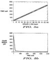
- the graphs in FIGs. 4a and 5a illustrate the frequency correction response to two different initial frequency and phase error according to an embodiment of the invention.
- the graphs in FIGs. 4b and 5b illustrate the phase correction response to an initial frequency and phase error according to an embodiment of the invention.
- the system 4 of three nodes shown in FIG. 1 had an initial 1% frequency error, basic 100Hz frequency, with one node with a 5ms initial phase error.
- the system 4 was set to the same initial settings with the link 31 between nodes N3 and N1 broken. It will be appreciated that the system 4 is fault tolerant and robust to any defects in inter-nodal links 12,23,31. Additionally, the embodiments of the invention discussed, a single fault such as due to a single faulty synchroniser will not crash the system or make the system fail.
- the foregoing embodiments may be implemented in hardware and/or software.
- a fairly accurate local clock for example 1% accuracy and 100 Hz (10 ms)
- the received signal is checked within a valid range, relative to the nodes local clock, where with a 1% accurate local clock the range may be +/-3%, where +/- 2% may be due to clock errors, and an extra 1% is allowed to correct phase errors when frequency may be at maximum difference.
- the receive time period is less than 9.7 or greater than 10.3, then the input is out of range, and this node will free run at its natural frequency.
- the frequency and phase locked loops are enabled, for example, locked is set to 1 in the pseudo code set out below. If the phase error, as shown as phaseerorror in the pseudo code below, between this nodes output and the input received is ⁇ 5 ⁇ s then both loops are locked, for example, locked is set to 2 in the pseudo code below. Both a frequency locked and phase locked loop is then applied to generate the output frequency, for example, shown as mytimeperiod in the pseudo code below, which is limited to +/- 2% of the nodes local clock before being output to another node.
Landscapes
- Engineering & Computer Science (AREA)
- Theoretical Computer Science (AREA)
- Computer Networks & Wireless Communication (AREA)
- Signal Processing (AREA)
- Physics & Mathematics (AREA)
- General Engineering & Computer Science (AREA)
- General Physics & Mathematics (AREA)
- Stabilization Of Oscillater, Synchronisation, Frequency Synthesizers (AREA)
- Hardware Redundancy (AREA)
- Synchronisation In Digital Transmission Systems (AREA)
Abstract
Description


Claims (8)
- A time synchronisation system (4) for use in a distributed computing system, the time synchronisation system comprising:at least two nodes (2,3), each node in communication with at least one other node via a signal synchroniser (10)in each node (2,3), each signal synchroniser (10) configured to analyse frequency and phase components of a received signal (20) from another node (2,3) to detect an error in accordance with a predetermined range in the frequency and phase components of a signal generated (28) by an oscillator (18) in the node (2,3) and to adjust the frequency and phase components of the generated signal (28).
- A time synchronisation system (4) as claimed in claim 1 wherein the signal synchroniser (10) further comprises a frequency error detector and corrector (13) and a phase error detector and corrector (14) for receiving the received signal (20) and for detecting errors in the frequency and phase to correct, and a combiner (16) to combine signals from the frequency and phase error detector and correctors (13,14) to the oscillator (18) in the node (2,3) for adjusting the frequency and phase components of the generated signal (20).
- A time synchronisation system (4) as claimed in claim 1 or 2 wherein the system comprises three nodes (1,2,3).
- A time synchronisation system (4) as claimed in any preceding claim wherein the system is arranged for use in an automotive application.
- A method for a time synchronisation system comprising the steps of:providing a distributed computing system (4) comprising at least two nodes (2,3), each node in communication with at least one other node via a signal synchroniser (10) in each node;analysing the frequency and phase components at each signal synchroniser (10) of a received signal (20) from another node;detecting an error in accordance with a predetermined range in the frequency and phase components of a signal (28) generated by an oscillator (18) in the node; and adjusting the frequency and phase components of the generated signal (28).
- A method for a time synchronisation system (4) as claimed in claim 5 wherein the detecting step further comprises providing the signal synchroniser (10) with a frequency error detector and corrector (13) and a phase error detector and corrector (14) for receiving the received signal (20) and detecting errors in the frequency and phase to correct, and a combiner (16) to combine signals from the frequency and phase error detector and correctors (13,14) to the oscillator (18) in the node (2,3) for adjusting the frequency and phase components of the generated signal (28).
- A method for a time synchronisation system as claimed in claim 4 or 5 wherein the providing a distributed computing system step comprises providing a system having at least three nodes (1,2,3).
- A method for a time synchronisation system as claimed in claims 4, 5 or 6 wherein the method is arranged for use in an automotive application.
Applications Claiming Priority (2)
| Application Number | Priority Date | Filing Date | Title |
|---|---|---|---|
| GB0116018 | 2001-07-02 | ||
| GB0116018A GB2377345B (en) | 2001-07-02 | 2001-07-02 | Time synchronisation system and method |
Publications (2)
| Publication Number | Publication Date |
|---|---|
| EP1274190A2 true EP1274190A2 (en) | 2003-01-08 |
| EP1274190A3 EP1274190A3 (en) | 2004-09-29 |
Family
ID=9917678
Family Applications (1)
| Application Number | Title | Priority Date | Filing Date |
|---|---|---|---|
| EP02014519A Withdrawn EP1274190A3 (en) | 2001-07-02 | 2002-07-01 | Time synchronisation system and method |
Country Status (3)
| Country | Link |
|---|---|
| US (1) | US20030079054A1 (en) |
| EP (1) | EP1274190A3 (en) |
| GB (1) | GB2377345B (en) |
Cited By (1)
| Publication number | Priority date | Publication date | Assignee | Title |
|---|---|---|---|---|
| EP1818742A2 (en) | 2006-02-14 | 2007-08-15 | Fanuc Ltd | Synchronizing control system for a plurality of controllers |
Families Citing this family (2)
| Publication number | Priority date | Publication date | Assignee | Title |
|---|---|---|---|---|
| KR100557112B1 (en) * | 2002-09-11 | 2006-03-03 | 삼성전자주식회사 | Device for estimating and combining frequency error at the receiving end of mobile communication system |
| PH12021552935A1 (en) | 2019-05-22 | 2022-07-25 | Vit Tall Llc | Multi-clock synchronization in power grids |
Family Cites Families (18)
| Publication number | Priority date | Publication date | Assignee | Title |
|---|---|---|---|---|
| US4369515A (en) * | 1980-10-06 | 1983-01-18 | Gte Automatic Electric Labs Inc. | Clock synchronization circuit |
| FR2495865A1 (en) * | 1980-12-09 | 1982-06-11 | Thomson Csf | DEVICE FOR RECOVERING A CLOCK SIGNAL FROM A BINARY SIGNAL AND A TRANSMISSION SYSTEM, IN PARTICULAR A DIGITAL MAGNETOSCOPE SYSTEM, COMPRISING SUCH A DEVICE |
| JPS5850827A (en) * | 1981-09-08 | 1983-03-25 | Fujitsu Ltd | Pll circuit |
| JPS60206339A (en) * | 1984-03-30 | 1985-10-17 | Victor Co Of Japan Ltd | Bit clock signal generator of digital signal demodulating device |
| US5526383A (en) * | 1992-08-14 | 1996-06-11 | Fujitsu Limited | Network control system for controlling relative errors between network nodes |
| US5278874A (en) * | 1992-09-02 | 1994-01-11 | Motorola, Inc. | Phase lock loop frequency correction circuit |
| US5509038A (en) * | 1994-04-06 | 1996-04-16 | Hal Computer Systems, Inc. | Multi-path data synchronizer system and method |
| EP0748093A1 (en) * | 1995-06-08 | 1996-12-11 | Laboratoires D'electronique Philips S.A.S. | Digital transmission system using decision means for selecting the synchronisation mode |
| US5907685A (en) * | 1995-08-04 | 1999-05-25 | Microsoft Corporation | System and method for synchronizing clocks in distributed computer nodes |
| KR100190032B1 (en) * | 1996-03-30 | 1999-06-01 | 윤종용 | Method for generating clock for recovering efm data and phase locked loop circuit thereof |
| JP2877198B2 (en) * | 1996-05-02 | 1999-03-31 | 日本電気株式会社 | Digital PLL circuit and start-up method thereof |
| JP3086173B2 (en) * | 1996-06-18 | 2000-09-11 | 日本無線株式会社 | Synchronization establishment method and data demodulation device using the same |
| JPH10107623A (en) * | 1996-10-01 | 1998-04-24 | Sony Corp | Conversion device and method, and PLL operation device and method |
| JPH10257041A (en) * | 1997-03-11 | 1998-09-25 | Sony Corp | Phase locked loop circuit and playback device |
| CN1163894C (en) * | 1998-12-17 | 2004-08-25 | 松下电器产业株式会社 | Frequency Control and Phase Synchronization Circuit |
| IL146180A0 (en) * | 1999-04-26 | 2002-07-25 | Computer Ass Think Inc | Method and appratus for maintaining data integrity across distributed computer systems |
| US6738429B1 (en) * | 1999-06-01 | 2004-05-18 | Harris Corporation | Decision-directed carrier frequency detector and method for QAM |
| US7035269B2 (en) * | 2000-02-02 | 2006-04-25 | Mcgill University | Method and apparatus for distributed synchronous clocking |
-
2001
- 2001-07-02 GB GB0116018A patent/GB2377345B/en not_active Expired - Fee Related
-
2002
- 2002-06-28 US US10/185,587 patent/US20030079054A1/en not_active Abandoned
- 2002-07-01 EP EP02014519A patent/EP1274190A3/en not_active Withdrawn
Cited By (2)
| Publication number | Priority date | Publication date | Assignee | Title |
|---|---|---|---|---|
| EP1818742A2 (en) | 2006-02-14 | 2007-08-15 | Fanuc Ltd | Synchronizing control system for a plurality of controllers |
| EP1818742A3 (en) * | 2006-02-14 | 2009-11-04 | Fanuc Ltd | Synchronizing control system for a plurality of controllers |
Also Published As
| Publication number | Publication date |
|---|---|
| GB2377345B (en) | 2004-06-16 |
| GB0116018D0 (en) | 2001-08-22 |
| EP1274190A3 (en) | 2004-09-29 |
| GB2377345A (en) | 2003-01-08 |
| US20030079054A1 (en) | 2003-04-24 |
Similar Documents
| Publication | Publication Date | Title |
|---|---|---|
| US6212660B1 (en) | Methods and apparatuses for identification of the position of data packets which are located in a serial received data stream | |
| US7979730B2 (en) | Method and device for synchronizing cycle time of a plurality of TTCAN buses based on determined global time deviations and a corresponding bus system | |
| US8675689B2 (en) | Method of time synchronization of free running nodes in an avionics network | |
| EP1852990B1 (en) | Device and method for time synchronization in distributed control system | |
| US6470458B1 (en) | Method and system for data processing system self-synchronization | |
| US8949648B2 (en) | System and method to overcome wander accumulation to achieve precision clock distribution over large networks | |
| US7594146B2 (en) | Apparatus, method, and program for correcting time of event trace data | |
| JPH10509294A (en) | System with predetermined timing relationship between data input and output, and transmitter and receiver of such system | |
| WO2001052417A2 (en) | Phase lock loop system and method | |
| CN102687401A (en) | System and method for selecting optimum local oscillator discipline source | |
| US20200382233A1 (en) | Information processing apparatus and time synchronization method | |
| EP1228412B1 (en) | System and method for fault-tolerant clock synchronization using interactive convergence | |
| CN102498671A (en) | Systems and methods for reducing delay duration | |
| JPH04363926A (en) | Digital data detection circuit and its detection method | |
| CA2757499A1 (en) | Water-base acrylic premanufactured waterproofing material and process for obtaining the same | |
| CN113302595A (en) | Multi-chip timing synchronization circuit and method | |
| EP1274190A2 (en) | Time synchronisation system and method | |
| US20040057539A1 (en) | Clock, data and time recovery using bit-resolved timing registers | |
| US7567630B2 (en) | Data processing device including clock recovery from various sources | |
| US7194650B2 (en) | System and method for synchronizing multiple synchronizer controllers | |
| US10110371B2 (en) | Phase difference estimation device and communication device having the phase difference estimation device | |
| JP2004153592A (en) | Pattern synchronization pull-in device and pattern synchronization pull-in method | |
| CN111865303B (en) | Clock phase discrimination method and device | |
| JP2690640B2 (en) | Missing clock detection circuit | |
| JP3282114B2 (en) | Clock tuning method |
Legal Events
| Date | Code | Title | Description |
|---|---|---|---|
| PUAI | Public reference made under article 153(3) epc to a published international application that has entered the european phase |
Free format text: ORIGINAL CODE: 0009012 |
|
| AK | Designated contracting states |
Kind code of ref document: A2 Designated state(s): AT BE BG CH CY CZ DE DK EE ES FI FR GB GR IE IT LI LU MC NL PT SE SK TR |
|
| AX | Request for extension of the european patent |
Free format text: AL;LT;LV;MK;RO;SI |
|
| PUAL | Search report despatched |
Free format text: ORIGINAL CODE: 0009013 |
|
| AK | Designated contracting states |
Kind code of ref document: A3 Designated state(s): AT BE BG CH CY CZ DE DK EE ES FI FR GB GR IE IT LI LU MC NL PT SE SK TR |
|
| AX | Request for extension of the european patent |
Extension state: AL LT LV MK RO SI |
|
| RIC1 | Information provided on ipc code assigned before grant |
Ipc: 7H 04L 12/42 B Ipc: 7G 06F 1/14 B Ipc: 7H 03L 7/113 B Ipc: 7B 60R 16/02 B Ipc: 7H 04L 12/413 B Ipc: 7H 04J 3/06 A |
|
| 17P | Request for examination filed |
Effective date: 20050114 |
|
| 17Q | First examination report despatched |
Effective date: 20050221 |
|
| AKX | Designation fees paid |
Designated state(s): DE FR GB IT |
|
| STAA | Information on the status of an ep patent application or granted ep patent |
Free format text: STATUS: THE APPLICATION IS DEEMED TO BE WITHDRAWN |
|
| 18D | Application deemed to be withdrawn |
Effective date: 20050705 |