EP1273181B1 - Splitter architecture for a telecommunication system - Google Patents
Splitter architecture for a telecommunication system Download PDFInfo
- Publication number
- EP1273181B1 EP1273181B1 EP01924848A EP01924848A EP1273181B1 EP 1273181 B1 EP1273181 B1 EP 1273181B1 EP 01924848 A EP01924848 A EP 01924848A EP 01924848 A EP01924848 A EP 01924848A EP 1273181 B1 EP1273181 B1 EP 1273181B1
- Authority
- EP
- European Patent Office
- Prior art keywords
- card
- splitter
- circuit board
- contacts
- signals
- Prior art date
- Legal status (The legal status is an assumption and is not a legal conclusion. Google has not performed a legal analysis and makes no representation as to the accuracy of the status listed.)
- Expired - Lifetime
Links
Images


Classifications
-
- H—ELECTRICITY
- H05—ELECTRIC TECHNIQUES NOT OTHERWISE PROVIDED FOR
- H05K—PRINTED CIRCUITS; CASINGS OR CONSTRUCTIONAL DETAILS OF ELECTRIC APPARATUS; MANUFACTURE OF ASSEMBLAGES OF ELECTRICAL COMPONENTS
- H05K7/00—Constructional details common to different types of electric apparatus
- H05K7/14—Mounting supporting structure in casing or on frame or rack
- H05K7/1438—Back panels or connecting means therefor; Terminals; Coding means to avoid wrong insertion
- H05K7/1459—Circuit configuration, e.g. routing signals
-
- H—ELECTRICITY
- H04—ELECTRIC COMMUNICATION TECHNIQUE
- H04Q—SELECTING
- H04Q1/00—Details of selecting apparatus or arrangements
- H04Q1/02—Constructional details
- H04Q1/028—Subscriber network interface devices
-
- H—ELECTRICITY
- H04—ELECTRIC COMMUNICATION TECHNIQUE
- H04Q—SELECTING
- H04Q1/00—Details of selecting apparatus or arrangements
- H04Q1/02—Constructional details
- H04Q1/10—Exchange station construction
-
- H—ELECTRICITY
- H04—ELECTRIC COMMUNICATION TECHNIQUE
- H04Q—SELECTING
- H04Q1/00—Details of selecting apparatus or arrangements
- H04Q1/02—Constructional details
- H04Q1/15—Backplane arrangements
- H04Q1/155—Backplane arrangements characterised by connection features
-
- H—ELECTRICITY
- H05—ELECTRIC TECHNIQUES NOT OTHERWISE PROVIDED FOR
- H05K—PRINTED CIRCUITS; CASINGS OR CONSTRUCTIONAL DETAILS OF ELECTRIC APPARATUS; MANUFACTURE OF ASSEMBLAGES OF ELECTRICAL COMPONENTS
- H05K1/00—Printed circuits
- H05K1/02—Details
- H05K1/11—Printed elements for providing electric connections to or between printed circuits
- H05K1/117—Pads along the edge of rigid circuit boards, e.g. for pluggable connectors
-
- H—ELECTRICITY
- H04—ELECTRIC COMMUNICATION TECHNIQUE
- H04Q—SELECTING
- H04Q1/00—Details of selecting apparatus or arrangements
- H04Q1/02—Constructional details
- H04Q1/14—Distribution frames
-
- H—ELECTRICITY
- H04—ELECTRIC COMMUNICATION TECHNIQUE
- H04Q—SELECTING
- H04Q2201/00—Constructional details of selecting arrangements
- H04Q2201/12—Printed circuits
-
- H—ELECTRICITY
- H04—ELECTRIC COMMUNICATION TECHNIQUE
- H04Q—SELECTING
- H04Q2201/00—Constructional details of selecting arrangements
- H04Q2201/80—Constructional details of selecting arrangements in specific systems
- H04Q2201/802—Constructional details of selecting arrangements in specific systems in data transmission systems
-
- H—ELECTRICITY
- H05—ELECTRIC TECHNIQUES NOT OTHERWISE PROVIDED FOR
- H05K—PRINTED CIRCUITS; CASINGS OR CONSTRUCTIONAL DETAILS OF ELECTRIC APPARATUS; MANUFACTURE OF ASSEMBLAGES OF ELECTRICAL COMPONENTS
- H05K1/00—Printed circuits
- H05K1/02—Details
- H05K1/0286—Programmable, customizable or modifiable circuits
- H05K1/0295—Programmable, customizable or modifiable circuits adapted for choosing between different types or different locations of mounted components
-
- H—ELECTRICITY
- H05—ELECTRIC TECHNIQUES NOT OTHERWISE PROVIDED FOR
- H05K—PRINTED CIRCUITS; CASINGS OR CONSTRUCTIONAL DETAILS OF ELECTRIC APPARATUS; MANUFACTURE OF ASSEMBLAGES OF ELECTRICAL COMPONENTS
- H05K1/00—Printed circuits
- H05K1/02—Details
- H05K1/14—Structural association of two or more printed circuits
-
- H—ELECTRICITY
- H05—ELECTRIC TECHNIQUES NOT OTHERWISE PROVIDED FOR
- H05K—PRINTED CIRCUITS; CASINGS OR CONSTRUCTIONAL DETAILS OF ELECTRIC APPARATUS; MANUFACTURE OF ASSEMBLAGES OF ELECTRICAL COMPONENTS
- H05K2201/00—Indexing scheme relating to printed circuits covered by H05K1/00
- H05K2201/09—Shape and layout
- H05K2201/09818—Shape or layout details not covered by a single group of H05K2201/09009 - H05K2201/09809
- H05K2201/09954—More mounting possibilities, e.g. on same place of PCB, or by using different sets of edge pads
-
- H—ELECTRICITY
- H05—ELECTRIC TECHNIQUES NOT OTHERWISE PROVIDED FOR
- H05K—PRINTED CIRCUITS; CASINGS OR CONSTRUCTIONAL DETAILS OF ELECTRIC APPARATUS; MANUFACTURE OF ASSEMBLAGES OF ELECTRICAL COMPONENTS
- H05K2201/00—Indexing scheme relating to printed circuits covered by H05K1/00
- H05K2201/10—Details of components or other objects attached to or integrated in a printed circuit board
- H05K2201/10227—Other objects, e.g. metallic pieces
- H05K2201/10356—Cables
Definitions
- Telecommunications systems commonly include cables containing bundles of twisted pairs of conductors for transmitting telecommunications signals (e.g ., voice only signals, data only signals, and combined/mixed voice and data signals, etc.).
- telecommunications signals e.g ., voice only signals, data only signals, and combined/mixed voice and data signals, etc.
- mating connectors e.g . , 25 pair Telco or Amp connectors
- the system may include an MDF (Main Distribution Frame), a POTS (Plain Old Telephone Service) splitter for separating voice and date signals, and a DSLAM (Digital Subscriber Line Access Multi-Plexer).
- MDF Main Distribution Frame
- POTS Plain Old Telephone Service
- DSLAM Digital Subscriber Line Access Multi-Plexer
- EP 0 909 102 which is considered as the closest prior art, discusses a splitter assembly comprising a circuit for combining or splitting POTS and XDSL signals from a single pair of wires. No discussion is presented as to extending this to a plurality of wire pairs running through interface contacts for splitting or combining of POTS and XDSL signals.
- One aspect of the present invention relates to a splitter architecture that accommodates both scalability and serviceability for voice band and ISDN (Integrated Services Digital Network) applications of a digital subscriber line (DSL), while fully supporting lifeline POTS and lifeline ISDN service requirements.
- the DSL's can include asymmetrical digital subscriber lines (ADSL) or very high speed digital subscriber lines (VDSL).
- Another aspect of the present invention relates to a telecommunications system capable of providing increased splitter densities.
- Still another aspect of the present invention relates to a telecommunications system including a splitter chassis having a back plane, and back plane interface cards mounted at generally perpendicular orientations relative to the back plane.
- the perpendicular orientation of the back plane interface cards provides for improved splitter densities, and also improves scalability by allowing the same type of back plane interface cards to be used with chassis of different sizes by merely varying the number of interface cards mounted within the chassis.
- Still another aspect of the present invention relates to aback plane interface card including card edge connectors for providing connections with a splitter card.
- the interface card also includes cable connectors for inputting mixed voice and data, and for outputting data signals and voice signals. Tracings are provided on the interface card for interconnecting the cable connectors and the card edge connectors. The tracings are configured such that first tracings carrying data signals from the splitter card to the cable connectors do not cross second tracings carrying voice signals from the splitter card to the cable connectors.
- a further aspect of the present invention relates to a telecommunications component including a circuit board, a first multi-pair cable connector, a second multi-pair cable connector, a third multi-pair connector and one or more card edge connectors.
- the first multi-pair connector is used to input twisted pair, mixed data/voice signal to the circuit board.
- the second multi-pair cable connector outputs twisted pair, voice signals from the circuit board.
- the third multi-pair cable connector outputs twisted pair, data signals from the circuit board.
- the signals are to be filtered at a downstream location (e.g., at a DSLAM)
- the third multi-pair connector can output mixed voice and data signals.
- the card edge connectors include a group of normally closed contacts, and a group of normally open contacts. All of the normally opened contacts are grouped separately from the normally closed contacts.
- First tracings are provided on the circuit board for connecting the first multi-pair cable connector to the normally closed contacts.
- Second tracings are provided on the circuit board for connecting the normally closed contacts to the second multi-pair cable connector.
- Third tracings are provided on the circuit board for connecting the normally open contacts to the third multi-pair cable connectors. The traces are positioned such that none of the third tracings on the circuit board cross over any of the first or second tracings.
- An additional aspect of the present invention relates to a chassis defining a back plane, and a back plane interface card mounted at the back plane of the chassis.
- the interface card includes a circuit board positioned at an orientation generally perpendicular with respect to the back plane.
- the interface card also includes a first multi-pair cable connector, a second multi-pair cable connector, a third multi-pair cable connector and one or more card edge connectors.
- the first multi-pair cable connector is positioned at the back plane for inputting twisted pair, mixed data/voice signals to the circuit board.
- the second multi-pair cable connector is positioned at the back plane for outputting twisted pair, voice signals from the circuit board.
- the third multi-pair cable connector is positioned at the back plane for outputting twisted pair, data signals or mixed data/voice signals, from the circuit board.
- the card edge connectors include normally closed contacts and normally open contacts. First tracings connect the first multi-pair cable connector to the normally closed contacts, second tracings connect the normally closed contacts to the second multi-pair connector cable, and third tracings connect the normally open contacts to the third multi-pair connector.
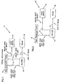
- a telecommunications system 10 including an arrangement of equipment.
- the system 10 is representative of a telephone carrier's system for transmitting voice and data to residences and businesses.
- a main distribution frame (MDF) 12 is linked to a splitter device 16 (e.g., a card including POTS splitter circuits or ISDN splitter circuits).
- the MDF 12 is also linked to one or more DSLAM modules 18, and a voice switch 19 (e.g., a switch equipped with POTS interface line cards or ISDN interface line cards).
- the splitter device 16 receives a mixed voice and data signal from the MDF 12.
- the splitter device 16 splits the mixed signal into split signals, and then filters the split signals. For example, one of the split signals can be filtered to provide a voice only signal (i.e., the high frequency data portion of the signal is filtered out), while the other split signal can be filtered to provide a data only signal (i.e., the low frequency voice portion of the signal is filtered out).
- the data only signals are passed from the splitter device 16 to the DSLAM 18.
- the voice only signals are passed from the splitter device 16 to the MDF 12 for transmission to the voice switch 19.
- Figure 2 shows a similar telecommunications system 10' having the same components as those described with respect to the telecommunications system 10' of Figure 1. However, in the embodiment of Figure 2, voice signals are transmitted directly from the splitter device 16 to the voice switch 19.
- the MDF 12, the POTS splitter device 16, the DSLAM 18 and the voice switch 19 are typically interconnected by cables 21.
- the cables 21 preferably each include multiple pairs of conductors for transmitting separate twisted pair signals.
- the cables 21 can comprise 25 pair cables (i.e., cables each containing 25 pairs of wire conductors for transmitting 25 separate twisted pair signals).
- Multi-pair connectors are used to provide interconnections between the cables 21 and the components of the telecommunications system 10.
- multi-pair connectors are typically provided at the ends of the cables 21.
- the multi-pair connectors at the ends of the cables 21 are commonly coupled to corresponding multi-pair cable connectors mounted at the equipment to provide connections thereinbetween.
- FIG. 3A and 3B An exemplary multi-pair cable connector 20 is shown in Figures 3A and 3B.
- the depicted connector 20 is a conventional connector such as a Telco or Amp connector.
- the connector 20 is adapted for use with a 25 pair cable.
- the conductor 20 preferably includes 25 pairs of conductors 28. For clarity, only two of the pairs of conductors 28 are shown in Figures 3A and 3B.
- the connector 20 includes a first end 26 defining a receptacle 27 sized for receiving a portion of a mating connector (not shown) connected at the end of a cable.
- the pairs of conductors 28 are positioned within the receptacle 27, and are adapted to contact corresponding conductor pairs of the mating connector.
- the conductors 28 extend through the connector 20 from the first end 26 to a second end 30. Portions of the conductors 28 located at the second end 30 are used to provide connections to conductor pairs of cables, wires, circuit boards, equipment, etc.
- the splitter 16 of Figs. 1 and 2 can be arranged in any number of known configurations.
- One known splitter configuration includes a chassis having a back plane.
- An interface card is mounted at the back plane.
- the interface card includes circuit board that is parallel to the back plane of the chassis.
- An array of cable connectors mounted on the circuit board.
- the array of cable connectors includes cable connectors for inputting mixed data/voice signals to the circuit board, cable connectors for outputting voice signals, and cable connectors for outputting data signals from the circuit board.
- Multiple sets of card edge connectors are provided on the circuit board for allowing multiple splitter cards to interface with the circuit board.
- the card edge connectors include a number of normal-through connections for providing full support of lifeline POTS and lifeline ISDN services.
- a plurality of tracings interconnect the array of cable connectors to the sets of card edge connectors.
- the tracings are arranged such that first tracings carrying data signals from the splitter cards cross over second tracings carrying voice signals from the splitter cards.
- the described crossing over of tracings may increase the cross talk that occurs at the back plane.
- the described crossing over of tracings requires the circuit board to have a relatively large number of layers thereby increasing the manufacturing costs associated with the circuit board.
- the configuration of the back plane interface card is not readily scalable because the size of the back plane circuit board will often need to be varied to be used with chassis of different sizes.
- FIGS 4A and 4B schematically illustrate a splitter architecture 40 in accordance with the principles of the present invention.
- the architecture 40 is particularly useful with telecommunication service options such as asymmetrical digital subscriber lines (ADSL) and very high speed digital subscriber lines (VDSL). While the signals in the schematics are shown traveling in one direction, it will be appreciated that the system is preferably bi-directional.
- ADSL digital subscriber lines
- VDSL very high speed digital subscriber lines
- the architecture 40 includes a back plane interface card 42 adapted to couple with a splitter card 44.
- the interface card 42 is preferably mounted at a back plane 46 of a splitter chassis or housing, and includes a circuit board 48 adapted to align at a generally perpendicular angle relative to the back plane 46.
- the circuit board 48 includes a back edge 50 positioned generally at the back plane 46, and a front edge 52 that is forwardly offset from the back plane 46.
- First, second and third multi-pair cable connectors 54, 56, and 58 are mounted at the back edge 50, and first and second card edge connectors 60 and 62 are mounted at the front edge 52.
- the first cable connector 54 (i.e., a LINE connector as labeled in Figure 8) is adapted for inputting twisted pair, mixed data/voice signals to the interface card 42.
- the second and third cable connectors 56 are used to respectively output twisted pair, voice signals and twisted pair data signals from the interface card 42.
- These connectors can be referred to as POTS (i.e., voice) and DATA Connectors as labeled in Figure 8.
- the connectors 54-58 can have the same configuration as the connector shown in Figures 3A and 3B. Referring to Figure 5D, a few representative conductors 28 are shown within the connectors 54-56.
- the first and second card edge connectors 60 and 62 are used to provide a connection between the interface card 42 and the splitter card 44.
- the splitter card 44 includes first and second card edge portions 64 and 66 that are respectively received within the first and second card edge connectors 60 and 62.
- the card edge portion 64 includes a pair of contacts 68b (e.g., contact pads) on one side of the splitter card 44, and another pair of contacts 70b (e.g., contact pads) on the other side of the splitter card 44.
- the contacts 68b and 70b engage respective contacts 68a and 70a of the first card edge connector 60.
- the contacts 68a and 70a are preferably spring contacts that normally engage one another (i.e., the contacts are normally closed).
- Figure 5C schematically shows a few representative contacts 68a and 70a.
- the second card edge portion 66 of the splitter card 44 includes contacts 72 (e.g., contact pads) for providing a connection with the second card edge connector 62.
- contacts 72 e.g., contact pads
- the contacts 72 engage respective contacts 74 provided at the second card edge connector 62 to provide a connection thereinbetween.
- the contacts 74 are preferably normally open (i.e., no signals are passed through the contacts 74 unless the splitter card 44 is coupled to the interface card 42).
- Figure 5C schematically shows a few representative few contacts 74. As shown in Figure 5C, the contacts 74 include two groups separated by a gap sized for receiving the card edge portion 66. Thus, the groups of contacts 74 are adapted for engaging contacts 72 located on opposite sides of the splitter card.
- the splitter architecture 40 has the capacity to process 24 separate twisted pair signals.
- the capacity of the splitter architecture 40 can be varied. For example, in certain embodiments it may be desirable to provide more or fewer splitters at the splitter card 44 (e.g., any number of splitters can be provided such as 8, 24, 48, 96, etc.). Thus, the number of separate circuit paths provided by the splitter architecture 40 can be varied accordingly.
- all of the contacts 68b and 70b are grouped separately from the contacts 72.
- all of the contacts 68b and 70b of the splitter card are preferably provided on the first card edge portion 64, while all of the contacts 72 of the splitter card are preferably provided at the second card edge portion 66.
- 48 of the contacts 72 can be provided at the second card edge portion 66, and 48 of each of the contacts 68b and 70b can be provided at the first card edge portion 64.
- the cable connector 54 is connected to the pair of contacts 68a by first tracings 76; the pair of contacts 70a is connected to cable connector 56 by second tracings 78; and the pair of contacts 74 is connected to cable connector 58 by third tracings 80.
- first tracings 76 the pair of contacts 70a is connected to cable connector 56 by second tracings 78; and the pair of contacts 74 is connected to cable connector 58 by third tracings 80.
- Figures 5A-5D show the back plane interface card 42 equipped with 24 separate circuits capable of handling 24 different twisted pair signals.
- all of the normally closed contacts 68a and 70a are provided at the first card edge connector 60, and all of the normally open contacts 74 are provided at card edge connector 62.
- the normally closed contacts 68a and 70a are grouped separately from the normally open contacts 74.
- This particular configuration is advantageous because a more simplified tracing layout can be used.
- the normally closed contacts 68a and 70a are grouped separately from the normally open contacts 74, none of the third tracings 80 are required to cross over any of the first or second tracings 76 and 78. This helps reduce manufacturing costs by reducing the number of layers required to manufacture the circuit board 48. Additionally, the reduction in crossing of the tracings may assist in reducing cross talk at the back plane 46.
- Figure 5E shows a multi-layer view of another interface card 42' constructed in accordance with the principles of the present invention.
- the card has a similar construction as the card 42 shown in Figures 5A-5D.
- both cards include cable connectors 54-56, as well as card edge connectors 60 and 62.
- card 42' has tracings 76', 78' and 80' that serve the same functions as tracings 76, 78 and 80 of the card 42; but are arranged in a slightly different pattern.
- tracings 76', 78' and 80' are preferably configured such that none of tracings 80' cross over any of tracings 76' and 78'.
- the normally open and closed contacts are grouped separately by placing such contacts on separate connectors. It will be appreciated that alternative grouping techniques can also be used. For example, the normally open and closed contacts can be separately grouped (i.e., not mixed or alternated) on a common connector. In one embodiment, all of the contacts can be grouped separately on a single connector. Additionally, for some applications, it may be desirable to use more than two connectors. For example, the group of normally closed connectors could be split between two connectors and the open contacts could be provided on a third connector.
- the splitter card 44 includes a plurality of splitters 82 (e.g., 24 splitters)
- the contacts 68b, 70b and 72 are shown connected to one of the splitters 82 by tracings.
- tracings 84 connect the contacts 68b to the splitter 82
- tracings 86 connect the contacts 70b to the splitter 82
- tracings 88 connect the contacts 72 to the splitter 82. While not shown for clarity purposes, it will be appreciated that similar contacts and tracings are provided for each of the twenty four splitters 82 shown in Figures 4A and 4B.
- the splitters 82 can have a number of different configurations.
- the splitters 82 can comprise POTS splitter circuits.
- a conventional POTS circuit functions to split a composite signal (i.e., a mixed voice/data signal) into two composite signals.
- One of the split composite signals is typically passed through one or more low pass filters capable of passing the relatively lower frequency voice content of the composite signal (e.g., less than about 4 kHz) and rejecting the composite signal content above the voice band (e.g., 30 kHz and above).
- the other split composite signal can be passed through a high pass filter that passes the composite signal content associated with the data band (e.g., about 30 kHz and above), and rejects the relatively lower frequency voice content of the composite signal.
- the other split signal can be unfiltered such that the signal remains a composite signal.
- the DSLAM or other digital multi-plexer that ultimately receives the composite signal will provide any required high-pass filter elements to remove the relatively low frequency voice signal content of the composite signal.
- ISDN filter circuits could also be used.
- Figures 4A and 4B show two modes of operation for the back plane interface card.
- Figure 4A shows the back plane interface card 42 in a normally closed mode in which the interface card 42 is not connected to the splitter card 44.
- an analog voice signal e.g., from an MDF
- the voice signal is transmitted through the first tracings 76 to contact 68a.
- the contacts 68a and 70a are closed.
- the voice signal is transmitted through the contacts 68a and 70a to the second tracings 78.
- the voice signal is transmitted through connector 56 and is outputted to another piece of equipment (e.g., an MDF or switch).
- another piece of equipment e.g., an MDF or switch.
- the normally closed contacts 68a and 70a at the card edge connector 60 fully support lifeline POTS and lifeline ISDN services.
- Figure 4B shows the splitter card 44 connected to interface card 42.
- the splitter card 44 When the splitter card 44 is connected to the interface card 42, the normally closed contacts 68a, 70a are opened and placed into respective engagement with contacts 68b and 70b of the splitter card 44. Also, contacts 74 of the second card edge connector 62 are concurrently closed (i.e., the contacts 74 are placed into engagement with contacts 72 of the splitter card 44).
- a composite signal inputted through connector 54 will be transmitted from cable connector 54 to the splitter 82 via tracings 76 and 84.
- the composite signal is preferably split and filtered such that a voice only signal is transmitted through tracings 86, and a data only signal is transmitted through tracings 88.
- the voice only signal is transmitted from tracings 86 through contacts 70b and 70a to tracings 78. From tracings 78, the voice only signal is outputted from cable connector 56 to a piece of equipment (e.g., an MDF or switch). The data only signal is transmitted through contacts 72 and 74 to tracings 80. From tracings 80, the data only signal is output through connector 58 to a piece of equipment (e.g., a DSLAM).
- a piece of equipment e.g., a DSLAM
- FIG. 6 is a schematic illustration showing the relative orientations between the back plane interface card 42 and the splitter card 44.
- the splitter card 44 when the splitter card 44 is connected to the interface card 42, the two cards are aligned generally parallel with respect to one another. Thus, as so positioned, both of the cards 42 and 44 are aligned perpendicular relative to the back plane 46 of the chassis.
- Such a configuration has been found to assist in greatly increasing the splitter density of a given chassis.
- Such a configuration also improves scalability by allowing the signal sized unifaced cards 42 to be used with chassis of different sizes. Further flexibility can be provided by either mounting the back plane interface cards 42 in a side by side relationship within a chassis, or by stacking the interface cards 42 one on top of the other within a chassis.
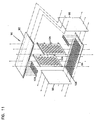
- FIG 7 illustrates a splitter chassis 90 constructed in accordance with the principles of the present invention.
- the chassis 90 is generally rectangular and includes a top side 92 positioned opposite from a bottom side 94. End plates 96 are provided for enclosing opposite ends of the chassis 90.
- a back plane plate 98 (as shown in Figure 8) defines a back plane of the chassis 90, and a front side 100 of the chassis 90 is generally open.
- the chassis 90 also includes mounting brackets 91 (shown in Figure 8) for connecting the chassis 90 to a structure such as a rack.
- a plurality of the back plane interface cards 42 are preferably secured to the back plane plate 98 by conventional techniques (e.g., fasteners such as bolts or screws).
- the back plane plate 98 defines multiple columns of vertically spaced apart openings 102 sized for receiving the cable connectors 54, 56 and 58 of the interface cards 42.
- the connectors define an array of connectors as shown in Figure 9.
- the chassis 90 includes intermediate dividers 104 that provide additional structural rigidity to the chassis 90.
- the chassis 90 also includes top and bottom tracks 106 and 108 respectively secured to the top side 92 and the bottom side 94 of the chassis 90.
- the top and the bottom tracks 106 and 108 oppose one another and define elongated slots that extend between the front and back sides of the chassis 90.
- the splitter cards 44 are mounted within the chassis 90 by sliding the splitter cards 44 through the open front side 100 into the tracks 106 and 108.
- top and bottom ends of the splitter cards 44 are respectively received within the upper and lower tracks 106 and 108.
- the tracks function to hold the splitter cards in a parallel, slightly spaced apart relation relative to one another.
- Front latches 110 on the splitter cards 44 hook into a top slot 112 of the chassis to retain the splitter cards 44 within the chassis 90.
- the back plane interface cards 42 are also mounted within the tracks 106 and 108.
- top and bottom edges of the interface cards 42 are received within the tracks 106 and 108.
- the tracks 106 and 108 assist in holding the back plane interface cards 42 in a perpendicular relationship relative to the back plane plate 98.
- the top and bottom tracks 106 and 108 also assist in maintaining a generally uniform spacing between the interface cards 42.
- each back plane interface card 42 is mounted in the same set of tracks as its corresponding splitter card 44. With such a configuration, the tracks 106 and 108 assist in providing registry between the interlace cards 42 and the splitter cards 44.
- FIGS 12-14 illustrate an alternative chassis 90' constructed in accordance with the principles of the present invention.
- the chassis 90' has a rectangular shape and is sized for receiving a single splitter card 44 and a single back plane interface 42. Similar to the chassis of Figure 7, the chassis 90' includes opposing tracks 106' and 108' for receiving the edges of the splitter card 44 and the interface card 42.
Abstract
Description
- This application is being filed as a PCT International Patent Application in the name of ADC Telecommunications, Inc., a U.S. national corporation, designating all countries except the US, on 09 April 2001.
- Telecommunications systems commonly include cables containing bundles of twisted pairs of conductors for transmitting telecommunications signals (e.g., voice only signals, data only signals, and combined/mixed voice and data signals, etc.). In these systems, mating connectors (e.g., 25 pair Telco or Amp connectors) are used to couple the cables to telecommunications equipment for processing. In a twisted pair telephone carrier system servicing residential and/or businesses, the system may include an MDF (Main Distribution Frame), a POTS (Plain Old Telephone Service) splitter for separating voice and date signals, and a DSLAM (Digital Subscriber Line Access Multi-Plexer). For most systems, it is desirable to maximize the splitter densities. Other important considerations include scalability, serviceability, reduction of cross-talk, ease of manufacture and cost.
EP 0 909 102, which is considered as the closest prior art, discusses a splitter assembly comprising a circuit for combining or splitting POTS and XDSL signals from a single pair of wires. No discussion is presented as to extending this to a plurality of wire pairs running through interface contacts for splitting or combining of POTS and XDSL signals. - One aspect of the present invention relates to a splitter architecture that accommodates both scalability and serviceability for voice band and ISDN (Integrated Services Digital Network) applications of a digital subscriber line (DSL), while fully supporting lifeline POTS and lifeline ISDN service requirements. By way of example, the DSL's can include asymmetrical digital subscriber lines (ADSL) or very high speed digital subscriber lines (VDSL).
- Another aspect of the present invention relates to a telecommunications system capable of providing increased splitter densities.
- Still another aspect of the present invention relates to a telecommunications system including a splitter chassis having a back plane, and back plane interface cards mounted at generally perpendicular orientations relative to the back plane. The perpendicular orientation of the back plane interface cards provides for improved splitter densities, and also improves scalability by allowing the same type of back plane interface cards to be used with chassis of different sizes by merely varying the number of interface cards mounted within the chassis.
- Still another aspect of the present invention relates to aback plane interface card including card edge connectors for providing connections with a splitter card. The interface card also includes cable connectors for inputting mixed voice and data, and for outputting data signals and voice signals. Tracings are provided on the interface card for interconnecting the cable connectors and the card edge connectors. The tracings are configured such that first tracings carrying data signals from the splitter card to the cable connectors do not cross second tracings carrying voice signals from the splitter card to the cable connectors.
- A further aspect of the present invention relates to a telecommunications component including a circuit board, a first multi-pair cable connector, a second multi-pair cable connector, a third multi-pair connector and one or more card edge connectors. The first multi-pair connector is used to input twisted pair, mixed data/voice signal to the circuit board. The second multi-pair cable connector outputs twisted pair, voice signals from the circuit board. The third multi-pair cable connector outputs twisted pair, data signals from the circuit board. Alternatively, if the signals are to be filtered at a downstream location (e.g., at a DSLAM), the third multi-pair connector can output mixed voice and data signals. The card edge connectors include a group of normally closed contacts, and a group of normally open contacts. All of the normally opened contacts are grouped separately from the normally closed contacts. First tracings are provided on the circuit board for connecting the first multi-pair cable connector to the normally closed contacts. Second tracings are provided on the circuit board for connecting the normally closed contacts to the second multi-pair cable connector. Third tracings are provided on the circuit board for connecting the normally open contacts to the third multi-pair cable connectors. The traces are positioned such that none of the third tracings on the circuit board cross over any of the first or second tracings.
- An additional aspect of the present invention relates to a chassis defining a back plane, and a back plane interface card mounted at the back plane of the chassis. The interface card includes a circuit board positioned at an orientation generally perpendicular with respect to the back plane. The interface card also includes a first multi-pair cable connector, a second multi-pair cable connector, a third multi-pair cable connector and one or more card edge connectors. The first multi-pair cable connector is positioned at the back plane for inputting twisted pair, mixed data/voice signals to the circuit board. The second multi-pair cable connector is positioned at the back plane for outputting twisted pair, voice signals from the circuit board. The third multi-pair cable connector is positioned at the back plane for outputting twisted pair, data signals or mixed data/voice signals, from the circuit board. The card edge connectors include normally closed contacts and normally open contacts. First tracings connect the first multi-pair cable connector to the normally closed contacts, second tracings connect the normally closed contacts to the second multi-pair connector cable, and third tracings connect the normally open contacts to the third multi-pair connector.
-
- Figure 1 is a diagram of a telecommunications system including an MDF, a splitter device, a DSLAM, and a voice switch;
- Figure 2 is another telecommunications system including an MDF, a splitter device, a DSLAM, and a voice switch;
- Figures 3A and 3B are front and side views of an exemplary twenty-five pair cable connector;
- Figure 4A is a schematic illustration of a back plane interface card and a splitter card constructed in accordance with the principles of the present invention, the back plane interface card is shown including normal-through connections for supporting lifeline services;
- Figure 4B shows the back plane connector card and the splitter card of Figure 4A interconnected together;
- Figures 5A and 5B are plan views of opposite sides of an interface card constructed in accordance with the principles of the present invention, the plan views show a representative tracing pattern;
- Figures 5C and 5D show end views of the interface card of Figures 5A and 5B;
- Figure 5E shows a multi-layer tracing layout for an interface card having a slightly different tracing pattern than the embodiment of Figures 5A and 5B;
- Figure 6 is a schematic depiction of an inventive configuration for a back plane interface card and a splitter card, both the back plane interface card and the splitter card are aligned at a generally perpendicular orientation relative to a chassis back plane;
- Figure 7 is a perspective view of a splitter chassis constructed in accordance with the principles of the present invention, an endplate of the chassis has been removed and a splitter card has been slid from the chassis;
- Figure 8 is a rear perspective view of the splitter chassis of Figure 7 with the back plane removed;
- Figure 9 is a rear view of the loaded splitter chassis of Figure 7;
- Figure 10 is a front view of the loaded splitter chassis of Figure 7;
- Figure 11 is an exploded view of the splitter chassis of Figure 7 with the splitter cards and the back plane interface cards removed;
- Figure 12 is a front perspective view of another chassis constructed in accordance with the principles of the present invention;
- Figure 13 is a rear perspective view of the splitter chassis of Figure 12; and
- Figure 14 is a front view of the splitter chassis of Figure 12.
- While the invention is amenable to various modifications and alternative forms, specifics thereof have been shown by way of example in the drawings and will be described in detail below. It is to be understood, however, that the intention is not to limit the invention to the particular embodiments described. On the contrary, the invention is intended to cover all modifications, equivalents, and alternatives falling within the scope of the invention as defined by the appended claims.
- In the following detailed description, references are made to the accompanying drawings that depict various embodiments in which the invention may be practiced. It is to be understood that other embodiments may be utilized, and structural and functional changes may be made without departing from the scope of the present invention.
- Referring now to Figure 1, a
telecommunications system 10 is shown including an arrangement of equipment. Thesystem 10 is representative of a telephone carrier's system for transmitting voice and data to residences and businesses. A main distribution frame (MDF) 12 is linked to a splitter device 16 (e.g., a card including POTS splitter circuits or ISDN splitter circuits). TheMDF 12 is also linked to one ormore DSLAM modules 18, and a voice switch 19 (e.g., a switch equipped with POTS interface line cards or ISDN interface line cards). - In use of the
system 10, thesplitter device 16 receives a mixed voice and data signal from theMDF 12. Thesplitter device 16 splits the mixed signal into split signals, and then filters the split signals. For example, one of the split signals can be filtered to provide a voice only signal (i.e., the high frequency data portion of the signal is filtered out), while the other split signal can be filtered to provide a data only signal (i.e., the low frequency voice portion of the signal is filtered out). The data only signals are passed from thesplitter device 16 to theDSLAM 18. The voice only signals are passed from thesplitter device 16 to theMDF 12 for transmission to thevoice switch 19. - Figure 2 shows a similar telecommunications system 10' having the same components as those described with respect to the telecommunications system 10' of Figure 1. However, in the embodiment of Figure 2, voice signals are transmitted directly from the
splitter device 16 to thevoice switch 19. - Referring still to Figs. 1 and 2, the
MDF 12, thePOTS splitter device 16, theDSLAM 18 and thevoice switch 19 are typically interconnected bycables 21. Thecables 21 preferably each include multiple pairs of conductors for transmitting separate twisted pair signals. By way of example, thecables 21 can comprise 25 pair cables (i.e., cables each containing 25 pairs of wire conductors for transmitting 25 separate twisted pair signals). Multi-pair connectors are used to provide interconnections between thecables 21 and the components of thetelecommunications system 10. For example, multi-pair connectors are typically provided at the ends of thecables 21. The multi-pair connectors at the ends of thecables 21 are commonly coupled to corresponding multi-pair cable connectors mounted at the equipment to provide connections thereinbetween. - An exemplary
multi-pair cable connector 20 is shown in Figures 3A and 3B. The depictedconnector 20 is a conventional connector such as a Telco or Amp connector. Preferably, theconnector 20 is adapted for use with a 25 pair cable. Thus, theconductor 20 preferably includes 25 pairs ofconductors 28. For clarity, only two of the pairs ofconductors 28 are shown in Figures 3A and 3B. - The
connector 20 includes afirst end 26 defining areceptacle 27 sized for receiving a portion of a mating connector (not shown) connected at the end of a cable. The pairs ofconductors 28 are positioned within thereceptacle 27, and are adapted to contact corresponding conductor pairs of the mating connector. Theconductors 28 extend through theconnector 20 from thefirst end 26 to asecond end 30. Portions of theconductors 28 located at thesecond end 30 are used to provide connections to conductor pairs of cables, wires, circuit boards, equipment, etc. - The
splitter 16 of Figs. 1 and 2 can be arranged in any number of known configurations. One known splitter configuration includes a chassis having a back plane. An interface card is mounted at the back plane. The interface card includes circuit board that is parallel to the back plane of the chassis. An array of cable connectors mounted on the circuit board. The array of cable connectors includes cable connectors for inputting mixed data/voice signals to the circuit board, cable connectors for outputting voice signals, and cable connectors for outputting data signals from the circuit board. Multiple sets of card edge connectors are provided on the circuit board for allowing multiple splitter cards to interface with the circuit board. The card edge connectors include a number of normal-through connections for providing full support of lifeline POTS and lifeline ISDN services. A plurality of tracings interconnect the array of cable connectors to the sets of card edge connectors. The tracings are arranged such that first tracings carrying data signals from the splitter cards cross over second tracings carrying voice signals from the splitter cards. - The above described configuration is problematic for a number of reasons. For example, the described crossing over of tracings may increase the cross talk that occurs at the back plane. Also, the described crossing over of tracings requires the circuit board to have a relatively large number of layers thereby increasing the manufacturing costs associated with the circuit board. Further, the configuration of the back plane interface card is not readily scalable because the size of the back plane circuit board will often need to be varied to be used with chassis of different sizes.
- Figures 4A and 4B schematically illustrate a
splitter architecture 40 in accordance with the principles of the present invention. Thearchitecture 40 is particularly useful with telecommunication service options such as asymmetrical digital subscriber lines (ADSL) and very high speed digital subscriber lines (VDSL). While the signals in the schematics are shown traveling in one direction, it will be appreciated that the system is preferably bi-directional. - The
architecture 40 includes a backplane interface card 42 adapted to couple with asplitter card 44. Theinterface card 42 is preferably mounted at aback plane 46 of a splitter chassis or housing, and includes acircuit board 48 adapted to align at a generally perpendicular angle relative to theback plane 46. Thecircuit board 48 includes aback edge 50 positioned generally at theback plane 46, and afront edge 52 that is forwardly offset from theback plane 46. First, second and thirdmulti-pair cable connectors back edge 50, and first and secondcard edge connectors front edge 52. The first cable connector 54 (i.e., a LINE connector as labeled in Figure 8) is adapted for inputting twisted pair, mixed data/voice signals to theinterface card 42. The second andthird cable connectors 56 are used to respectively output twisted pair, voice signals and twisted pair data signals from theinterface card 42. These connectors can be referred to as POTS (i.e., voice) and DATA Connectors as labeled in Figure 8. The connectors 54-58 can have the same configuration as the connector shown in Figures 3A and 3B. Referring to Figure 5D, a fewrepresentative conductors 28 are shown within the connectors 54-56. - The first and second
card edge connectors interface card 42 and thesplitter card 44. For example, thesplitter card 44 includes first and secondcard edge portions card edge connectors card edge portion 64 includes a pair ofcontacts 68b (e.g., contact pads) on one side of thesplitter card 44, and another pair ofcontacts 70b (e.g., contact pads) on the other side of thesplitter card 44. When the firstcard edge portion 64 is inserted within the firstcard edge connector 60, thecontacts respective contacts card edge connector 60. Thecontacts representative contacts card edge portion 64 is inserted within the firstcard edge connector 60, thecontacts contacts - Referring again to Figures 4A and 4B, the second
card edge portion 66 of thesplitter card 44 includes contacts 72 (e.g., contact pads) for providing a connection with the secondcard edge connector 62. For example, when the secondcard edge portion 66 is inserted into the secondcard edge connector 62, thecontacts 72 engagerespective contacts 74 provided at the secondcard edge connector 62 to provide a connection thereinbetween. Thecontacts 74 are preferably normally open (i.e., no signals are passed through thecontacts 74 unless thesplitter card 44 is coupled to the interface card 42). Figure 5C schematically shows a few representativefew contacts 74. As shown in Figure 5C, thecontacts 74 include two groups separated by a gap sized for receiving thecard edge portion 66. Thus, the groups ofcontacts 74 are adapted for engagingcontacts 72 located on opposite sides of the splitter card. - For clarity purposes, only one twisted pair circuit for the splitter architecture is shown in Figures 4A and 4B. Thus, only single pairs of the
contacts connectors splitter card 44. For example, if the cable connectors 54-56 and 58 comprise conventional 25 pair connectors, 24 separate pairs of thecontacts splitter architecture 40 has the capacity to process 24 separate twisted pair signals. Of course, the capacity of thesplitter architecture 40 can be varied. For example, in certain embodiments it may be desirable to provide more or fewer splitters at the splitter card 44 (e.g., any number of splitters can be provided such as 8, 24, 48, 96, etc.). Thus, the number of separate circuit paths provided by thesplitter architecture 40 can be varied accordingly. - With respect to the
splitter card 44, it is preferred for all of thecontacts contacts 72. For example, all of thecontacts card edge portion 64, while all of thecontacts 72 of the splitter card are preferably provided at the secondcard edge portion 66. In a card with 24 splitters, 48 of thecontacts 72 can be provided at the secondcard edge portion contacts card edge portion 64. - Referring still to Figures 4A and 4B, the
cable connector 54 is connected to the pair ofcontacts 68a byfirst tracings 76; the pair ofcontacts 70a is connected tocable connector 56 bysecond tracings 78; and the pair ofcontacts 74 is connected tocable connector 58 bythird tracings 80. Once again, for clarity and ease of explanation, the circuit pathway for only a single twisted pair signal has been illustrated in Figures 4A and 4B. - Figures 5A-5D show the back
plane interface card 42 equipped with 24 separate circuits capable of handling 24 different twisted pair signals. In the embodiment of Figures 5A-5D, all of the normally closedcontacts card edge connector 60, and all of the normallyopen contacts 74 are provided atcard edge connector 62. Thus, the normally closedcontacts open contacts 74. This particular configuration is advantageous because a more simplified tracing layout can be used. For example, because the normally closedcontacts open contacts 74, none of thethird tracings 80 are required to cross over any of the first orsecond tracings circuit board 48. Additionally, the reduction in crossing of the tracings may assist in reducing cross talk at theback plane 46. - Figure 5E shows a multi-layer view of another interface card 42' constructed in accordance with the principles of the present invention. The card has a similar construction as the
card 42 shown in Figures 5A-5D. For example, both cards include cable connectors 54-56, as well ascard edge connectors tracings card 42; but are arranged in a slightly different pattern. As previously described with respect to tracings 76-80, tracings 76', 78' and 80' are preferably configured such that none of tracings 80' cross over any of tracings 76' and 78'. - As shown in Figures 5A-5E, the normally open and closed contacts are grouped separately by placing such contacts on separate connectors. It will be appreciated that alternative grouping techniques can also be used. For example, the normally open and closed contacts can be separately grouped (i.e., not mixed or alternated) on a common connector. In one embodiment, all of the contacts can be grouped separately on a single connector. Additionally, for some applications, it may be desirable to use more than two connectors. For example, the group of normally closed connectors could be split between two connectors and the open contacts could be provided on a third connector.
- Referring back to Figures 4A and 4B, the
splitter card 44 includes a plurality of splitters 82 (e.g., 24 splitters) Thecontacts splitters 82 by tracings. For example,tracings 84 connect thecontacts 68b to thesplitter 82,tracings 86 connect thecontacts 70b to thesplitter 82, andtracings 88 connect thecontacts 72 to thesplitter 82. While not shown for clarity purposes, it will be appreciated that similar contacts and tracings are provided for each of the twenty foursplitters 82 shown in Figures 4A and 4B. - The
splitters 82 can have a number of different configurations. For example, thesplitters 82 can comprise POTS splitter circuits. A conventional POTS circuit functions to split a composite signal (i.e., a mixed voice/data signal) into two composite signals. One of the split composite signals is typically passed through one or more low pass filters capable of passing the relatively lower frequency voice content of the composite signal (e.g., less than about 4 kHz) and rejecting the composite signal content above the voice band (e.g., 30 kHz and above). The other split composite signal can be passed through a high pass filter that passes the composite signal content associated with the data band (e.g., about 30 kHz and above), and rejects the relatively lower frequency voice content of the composite signal. Alternatively, the other split signal can be unfiltered such that the signal remains a composite signal. For such an embodiment, it is assumed that the DSLAM or other digital multi-plexer that ultimately receives the composite signal will provide any required high-pass filter elements to remove the relatively low frequency voice signal content of the composite signal. It will further be appreciated that ISDN filter circuits could also be used. - Figures 4A and 4B show two modes of operation for the back plane interface card. Figure 4A shows the back
plane interface card 42 in a normally closed mode in which theinterface card 42 is not connected to thesplitter card 44. In such a mode, an analog voice signal (e.g., from an MDF) is inputted to theinterface card 42 throughconnector 54. Once at theinterface card 42, the voice signal is transmitted through thefirst tracings 76 to contact 68a. Because thesplitter card 44 is not connected to theinterface card 42, thecontacts contacts second tracings 78. From thesecond tracings 78, the voice signal is transmitted throughconnector 56 and is outputted to another piece of equipment (e.g., an MDF or switch). In this manner, the normally closedcontacts card edge connector 60 fully support lifeline POTS and lifeline ISDN services. - Figure 4B shows the
splitter card 44 connected to interfacecard 42. When thesplitter card 44 is connected to theinterface card 42, the normally closedcontacts contacts splitter card 44. Also,contacts 74 of the secondcard edge connector 62 are concurrently closed (i.e., thecontacts 74 are placed into engagement withcontacts 72 of the splitter card 44). Thus, a composite signal inputted throughconnector 54 will be transmitted fromcable connector 54 to thesplitter 82 viatracings splitter 82, the composite signal is preferably split and filtered such that a voice only signal is transmitted throughtracings 86, and a data only signal is transmitted throughtracings 88. The voice only signal is transmitted fromtracings 86 throughcontacts tracings 78, the voice only signal is outputted fromcable connector 56 to a piece of equipment (e.g., an MDF or switch). The data only signal is transmitted throughcontacts tracings 80, the data only signal is output throughconnector 58 to a piece of equipment (e.g., a DSLAM). - Figure 6 is a schematic illustration showing the relative orientations between the back
plane interface card 42 and thesplitter card 44. As shown, when thesplitter card 44 is connected to theinterface card 42, the two cards are aligned generally parallel with respect to one another. Thus, as so positioned, both of thecards back plane 46 of the chassis. Such a configuration has been found to assist in greatly increasing the splitter density of a given chassis. Such a configuration also improves scalability by allowing the signal sizedunifaced cards 42 to be used with chassis of different sizes. Further flexibility can be provided by either mounting the backplane interface cards 42 in a side by side relationship within a chassis, or by stacking theinterface cards 42 one on top of the other within a chassis. - Figure 7 illustrates a
splitter chassis 90 constructed in accordance with the principles of the present invention. Thechassis 90 is generally rectangular and includes atop side 92 positioned opposite from abottom side 94.End plates 96 are provided for enclosing opposite ends of thechassis 90. A back plane plate 98 (as shown in Figure 8) defines a back plane of thechassis 90, and afront side 100 of thechassis 90 is generally open. Thechassis 90 also includes mounting brackets 91 (shown in Figure 8) for connecting thechassis 90 to a structure such as a rack. - As best shown in Figure 8, a plurality of the back
plane interface cards 42 are preferably secured to theback plane plate 98 by conventional techniques (e.g., fasteners such as bolts or screws). Theback plane plate 98 defines multiple columns of vertically spaced apartopenings 102 sized for receiving thecable connectors interface cards 42. When theinterface cards 42 are connected to theback plane plate 98, the connectors define an array of connectors as shown in Figure 9. - Referring to Figure 11, the
chassis 90 includesintermediate dividers 104 that provide additional structural rigidity to thechassis 90. Thechassis 90 also includes top andbottom tracks top side 92 and thebottom side 94 of thechassis 90. The top and the bottom tracks 106 and 108 oppose one another and define elongated slots that extend between the front and back sides of thechassis 90. As shown in Figure 7, thesplitter cards 44 are mounted within thechassis 90 by sliding thesplitter cards 44 through the openfront side 100 into thetracks splitter cards 44 are respectively received within the upper andlower tracks splitter cards 44 hook into atop slot 112 of the chassis to retain thesplitter cards 44 within thechassis 90. - As best shown in Figures 7 and 10, the back
plane interface cards 42 are also mounted within thetracks interface cards 42 are received within thetracks tracks plane interface cards 42 in a perpendicular relationship relative to theback plane plate 98. The top andbottom tracks interface cards 42. Preferably, each backplane interface card 42 is mounted in the same set of tracks as itscorresponding splitter card 44. With such a configuration, thetracks interlace cards 42 and thesplitter cards 44. - Figures 12-14 illustrate an alternative chassis 90' constructed in accordance with the principles of the present invention. The chassis 90' has a rectangular shape and is sized for receiving a
single splitter card 44 and a singleback plane interface 42. Similar to the chassis of Figure 7, the chassis 90' includes opposing tracks 106' and 108' for receiving the edges of thesplitter card 44 and theinterface card 42. - The above specification, examples and data provide a complete description of the manufacture and use of the composition of the invention. Since many embodiments of the invention can be made without departing from the scope of the invention, the invention resides in the claims hereinafter appended
Claims (23)
- A telecommunications component comprising:a circuit board (48);a first multi-pair cable connector (54) for inputting twisted pair, mixed data/voice signals to the circuit board (48);a second multi-pair cable connector (56) for outputting twisted pair, voice signals from the circuit board (48);a third multi-pair cable connector (58) for outputting twisted pair, data signals or mixed data/voice signals from the circuit board (48);one or more card edge connectors (60, 62) connected to the circuit board (48), the one or more card edge connectors (60, 62) including:the tracings (76, 78, 80) being positioned such that none of the third tracings (80) on the circuit board (48) cross-over any of the first or second tracings (76, 78).a group of normally closed contacts (68a, 70a);a group of normally open contacts (74), all of the normally open contacts (74) being grouped separately from the normally closed contacts (68a, 70a);first tracings (76) provided on the circuit board (48) for connecting the first multi-pair cable connector (54) to the normally closed contacts (68a, 70a);second tracings (78) provided on the circuit board (48) for connecting the normally closed contacts (68a, 70a) to the second multi-pair cable connector (56);third tracings (80) provided on the circuit board (48) for connecting the normally open contacts (74) to the third multi-pair cable connector (58); and
- The telecommunications component of claim 1, further comprising a splitter card (44) adapted for connection to the one or more card edge connectors (60, 62) of the circuit board (48), the splitter card (44) including a plurality of splitters (82) for splitting the mixed data/voice signals into the data signals and the voice signals.
- The telecommunications component of claim 2, wherein the splitters (82) comprise POTS splitters.
- The telecommunications component of claim 3, wherein the splitter card (44) includes at least 24 of the POTS splitters.
- The telecommunications component of any of the preceding claims, wherein the one or more card edge connectors (60, 62) include a first card edge connector (60) and a separate second card edge connector (62), the first card connector (60) including the normally closed contacts (68a, 70a) and the second card edge connector (62) including the normally open contacts (74).
- The telecommunications component of claim 5, further comprising a splitter card (44) adapted for connection to the first and second card edge connectors (60, 62) of the circuit board (48), the splitter card (44) including a plurality of splitters (82) for splitting the mixed data/voice signals into the data signals and the voice signals.
- The telecommunications component of claim 6, wherein the splitters (82) comprise POTS splitters.
- The telecommunications component of claim 7, wherein the splitter card (44) includes at least 24 of the POTS splitters.
- The telecommunications component of any of the preceding claims, further comprising a chassis (90) including a reference back plane (98) at which the first, second and third multi-pair cable connectors (54, 56, 58) are positioned, the circuit board (48) being aligned generally at a perpendicular orientation relative to the reference back plane (98).
- The telecommunications component of claim 9, further comprising a splitter card (44) adapted for connection to the one or more card edge connectors (60, 62) of the circuit board (48), the splitter card (44) including a plurality of splitters (82) for splitting the mixed data/voice signals into the data signals and the voice signals, the splitter card (44) being aligned at a generally parallel orientation relative to the circuit board (48) when the splitter card (44) is connected to the one or more card edge connectors (60, 62).
- The telecommunications component of claim 10, wherein the splitters (82) comprise POTS splitters.
- The telecommunications component of claim 11, wherein the splitter card (44) includes at least 24 of the POTS splitters.
- The telecommunications component of any of claims 9 to 12, wherein the chassis (90) includes opposing slots, wherein the circuit board (48) is mounted in the slots.
- The telecommunications component of claim 13, further comprising a splitter card (44) adapted for connection to the one or more card edge connectors (60, 62) of the circuit board (48), the splitter card (44) including a plurality of splitters (82) for splitting the mixed data/voice signals into the data signals and the voice signals, the splitter card (44) and the circuit board (48) being mounted in the same opposing slots when the splitter card (44) is connected to the circuit board (48) by the first and second card edge connectors (60, 62).
- A telecommunications component of claim 9, wherein the circuit board (48), the first, second and third multi-pair cable connector (54, 56, 58) and one or more edge connectors (60, 62) make-up an interface card (42).
- The telecommunications component of claim 15, wherein a plurality of the interface cards (42) are mounted within the chassis (90).
- The telecommunications component of claim 16, wherein a plurality of the interface cards (42) include 24 generally parallel interface cards (42).
- The telecommunications component of claim 15, wherein the chassis (90) is sized to hold a single one of the interface card (42).
- The telecommunications component of any of claims 15 to 18, further comprising a plurality of splitter cards (44) mounted in the chassis (90) and electrically connected to the card edge connectors (60, 62) of the interface cards (42).
- A splitter card (44) comprisinga circuit board (44);a plurality of splitters (82) mounted on the circuit board (44), each splitter being adapted for receiving mixed voice and data signals and outputting first signals that are voice only and second signals that are data only or mixed voice and data;a first card extension (64) adapted to be received in a card edge connector (60), the first card extension (64) including first contacts (68b) for receiving the mixed voice and data signals and second contacts (70b) for outputting the first signals;a second card extension (66) adapted to be received in a card edge connector (62), the second card extension including third contacts (72) for outputting the second signals;first tracings (84) for transmitting the mixed voice and data signals from the first contacts (68b) to the splitters (82);second tracings (86) for transmitting the first signals from the splitters (82) to the second contacts (70b);third tracings (88) for transmitting the second signals from the splitters (82) to the third contacts (72); andall of the first and second contacts (68b, 70b) being located at the first extension (64) and all of the third contacts (72) being located at the second extension (68), wherein the first and second contacts (68b, 70b) are grouped together at a location separate from the third contacts (72).
- The splitter card (44) of claim 20, wherein 24 of the splitters (82) are provided on the circuit board.
- A telecommunications chassis (90) assembly comprising;a chassis (90) defining a reference back plane (46);one or more printed circuit boards (48) positioned adjacent the reference back plane (46);a plurality of multi-pair line connectors (54) for inputting twisted pair, mixed data/voice signals to the one or more circuit boards (48);a plurality of multi-pair voice connectors (56) for outputting twisted pair, voice signals from the one or more circuit boards (48);a plurality of multi-pair data connectors (58) for outputting twisted pair, data signals or mixed data/voice signals from the one or more circuit boards (48);a first row of card edge connectors positioned within the chassis (60);a second row of card edge connectors positioned within the chassis (62);the line and voice connectors (54, 56) being electrically connected by the one or more circuit boards (48) exclusively to the first row of card edge connectors (60); andthe data connectors (58) being electrically connected by the one or more circuit boards (48) exclusively to the second row of card edge connectors (62).
- The telecommunications chassis (90) assembly of claim 22, wherein the first and second rows are horizontal rows.
Applications Claiming Priority (3)
| Application Number | Priority Date | Filing Date | Title |
|---|---|---|---|
| US549133 | 1983-11-07 | ||
| US09/549,133 US7333606B1 (en) | 2000-04-13 | 2000-04-13 | Splitter architecture for a telecommunications system |
| PCT/US2001/011494 WO2001080574A2 (en) | 2000-04-13 | 2001-04-09 | Splitter architecture for a telecommunication system |
Publications (2)
| Publication Number | Publication Date |
|---|---|
| EP1273181A2 EP1273181A2 (en) | 2003-01-08 |
| EP1273181B1 true EP1273181B1 (en) | 2006-03-29 |
Family
ID=24191801
Family Applications (1)
| Application Number | Title | Priority Date | Filing Date |
|---|---|---|---|
| EP01924848A Expired - Lifetime EP1273181B1 (en) | 2000-04-13 | 2001-04-09 | Splitter architecture for a telecommunication system |
Country Status (8)
| Country | Link |
|---|---|
| US (2) | US7333606B1 (en) |
| EP (1) | EP1273181B1 (en) |
| AT (1) | ATE322128T1 (en) |
| AU (2) | AU2001251465B2 (en) |
| CA (1) | CA2406246A1 (en) |
| DE (1) | DE60118353D1 (en) |
| TW (1) | TW521528B (en) |
| WO (1) | WO2001080574A2 (en) |
Families Citing this family (38)
| Publication number | Priority date | Publication date | Assignee | Title |
|---|---|---|---|---|
| US7333606B1 (en) * | 2000-04-13 | 2008-02-19 | Adc Telecommunications, Inc. | Splitter architecture for a telecommunications system |
| DE20104605U1 (en) | 2001-03-16 | 2001-05-31 | 3M Innovative Properties Co | Terminal block and distribution device |
| US7257223B2 (en) | 2001-05-10 | 2007-08-14 | Adc Telecommunications, Inc. | Splitter assembly for a telecommunications system |
| US6628525B2 (en) | 2001-06-29 | 2003-09-30 | Adc Telecommunications, Inc. | Card guide for a telecommunications splitter assembly |
| US6804352B2 (en) | 2001-06-29 | 2004-10-12 | Adc Telecommunications, Inc. | High circuit density pots splitter assembly |
| US6738463B2 (en) | 2001-06-29 | 2004-05-18 | Adc Telecommunications, Inc. | Splitter assembly with inverted pots and line connectors |
| US6804353B2 (en) | 2001-06-29 | 2004-10-12 | Adc Telecommunications, Inc. | Splitter assembly with high density backplane board |
| ITTO20020178U1 (en) * | 2002-10-04 | 2004-04-05 | Urmet Sistemi S P A | SYSTEM OF POTS-SPLITTER FILTER MODULES FOR ADSL. |
| US7463722B2 (en) * | 2002-10-18 | 2008-12-09 | Adc Telecommunications, Inc. | Splitter system with test access |
| US6885798B2 (en) | 2003-09-08 | 2005-04-26 | Adc Telecommunications, Inc. | Fiber optic cable and furcation module |
| FR2863409B1 (en) * | 2003-12-09 | 2009-01-23 | Nexans | CABLE INTERCONNECTION MODULE AND REGULATOR |
| US7660409B1 (en) * | 2004-05-25 | 2010-02-09 | Alcatel Lucent | Multi-dwelling unit module for passive optical networks |
| US7376322B2 (en) * | 2004-11-03 | 2008-05-20 | Adc Telecommunications, Inc. | Fiber optic module and system including rear connectors |
| US7418181B2 (en) | 2006-02-13 | 2008-08-26 | Adc Telecommunications, Inc. | Fiber optic splitter module |
| CN1941650B (en) * | 2006-09-22 | 2010-05-12 | 华为技术有限公司 | Signal separation method and separating system and separator board |
| DE202006016752U1 (en) * | 2006-10-30 | 2007-02-01 | CCS Technology, Inc., Wilmington | Distributing device e.g. distributor cabinet, for use in telecommunication arrangement, has digital subscriber line access multiplier-data signaling lines leading to plug-in connector units and intercepted in intercepting devices |
| FR2927222B1 (en) * | 2008-02-05 | 2010-10-15 | Thales Sa | ARRANGEMENT OF AVIONIC RACK |
| US20100128447A1 (en) * | 2008-11-21 | 2010-05-27 | Tyco Electronics Corporation | Memory module having voltage regulator module |
| EP2564250A4 (en) | 2010-04-27 | 2013-11-13 | Adc Comm Shanghai Co Ltd | Fiber optic module and chassis |
| US9182563B2 (en) | 2011-03-31 | 2015-11-10 | Adc Telecommunications, Inc. | Adapter plate for fiber optic module |
| US9417401B2 (en) | 2011-09-06 | 2016-08-16 | Commscope Technologies Llc | Adapter for fiber optic module |
| US9477287B1 (en) * | 2012-06-28 | 2016-10-25 | Amazon Technologies, Inc. | Optimizing computing resources |
| CN105324696B (en) | 2012-12-19 | 2019-05-17 | 泰科电子瑞侃有限公司 | Distributor with the splitter gradually increased |
| US9451719B2 (en) * | 2013-08-29 | 2016-09-20 | Abb Technology Ag | U form-factor intelligent electronic device (IED) hardware platform with matching of IED wiring, from a non U form-factor IED hardware platform using adapter structure |
| US9301030B2 (en) | 2013-11-11 | 2016-03-29 | Commscope Technologies Llc | Telecommunications module |
| EP3158377B1 (en) | 2014-06-17 | 2022-02-23 | CommScope Connectivity Belgium BVBA | Cable distribution system |
| WO2015200321A1 (en) | 2014-06-23 | 2015-12-30 | Adc Telecommunications, Inc. | Fiber cable fan-out assembly and method |
| US10054753B2 (en) | 2014-10-27 | 2018-08-21 | Commscope Technologies Llc | Fiber optic cable with flexible conduit |
| AU2015207954C1 (en) | 2015-07-31 | 2022-05-05 | Adc Communications (Australia) Pty Limited | Cable breakout assembly |
| US10162131B2 (en) | 2015-08-21 | 2018-12-25 | Commscope Technologies Llc | Telecommunications module |
| US10606009B2 (en) | 2015-12-01 | 2020-03-31 | CommScope Connectivity Belgium BVBA | Cable distribution system with fan out devices |
| US10637220B2 (en) | 2016-01-28 | 2020-04-28 | CommScope Connectivity Belgium BVBA | Modular hybrid closure |
| US11131821B2 (en) | 2016-03-18 | 2021-09-28 | Commscope Technologies Llc | Optic fiber cable fanout conduit arrangements; components, and methods |
| US10222571B2 (en) | 2016-04-07 | 2019-03-05 | Commscope Technologies Llc | Telecommunications module and frame |
| EP3507633A4 (en) | 2016-08-31 | 2020-04-01 | Commscope Technologies LLC | Fiber optic cable clamp and clamp assembly |
| WO2018071481A1 (en) | 2016-10-13 | 2018-04-19 | Commscope Technologies Llc | Fiber optic breakout transition assembly incorporating epoxy plug and cable strain relief |
| WO2018134651A1 (en) * | 2017-01-17 | 2018-07-26 | Shams Ali | Professional and secure terminal splitter for adsl optimized wiring mdf |
| US11131822B2 (en) | 2017-05-08 | 2021-09-28 | Commscope Technologies Llc | Fiber-optic breakout transition assembly |
Family Cites Families (39)
| Publication number | Priority date | Publication date | Assignee | Title |
|---|---|---|---|---|
| US4476357A (en) * | 1982-09-28 | 1984-10-09 | T-Bar Incorporated | Switching apparatus employing conductor contracts on a movable elastomeric member |
| US4552420A (en) * | 1983-12-02 | 1985-11-12 | E. I. Du Pont De Nemours And Company | Electrical connector using a flexible circuit having an impedance control arrangement thereon |
| US4824383A (en) * | 1986-11-18 | 1989-04-25 | E. I. Du Pont De Nemours And Company | Terminator and corresponding receptacle for multiple electrical conductors |
| US4815104A (en) | 1988-01-11 | 1989-03-21 | Telect, Inc. | Digital telecommunications network, cross-connect module |
| US4821150A (en) * | 1988-03-31 | 1989-04-11 | Hubbell Incorporated | Printed circuit board mounting for communication termination |
| US4975072A (en) | 1989-10-25 | 1990-12-04 | Telect, Inc. | Front facing terminal block for telecommunication main distribution frame |
| JPH04340795A (en) | 1991-05-17 | 1992-11-27 | Mitsubishi Electric Corp | Printed circuit board |
| US5209678A (en) | 1992-01-09 | 1993-05-11 | Telect, Inc. | Telecommunications front access coaxial jack and plug assembly with releasable locking feature |
| US5233501A (en) | 1992-02-27 | 1993-08-03 | Telect, Inc. | Digital telecommunication network cross-connect module having a printed circuit board connected to jack switches |
| US5719933A (en) * | 1994-02-18 | 1998-02-17 | Welch; Richard | Wiring arrangement for a communication interconnection system |
| US5546282A (en) | 1995-05-02 | 1996-08-13 | Telect, Inc. | Telecommunication network digital cross-connect panels having insertable modules with printed circuit board mounted coaxial jack switches |
| JP2638567B2 (en) | 1995-06-08 | 1997-08-06 | 日本電気株式会社 | Multilayer wiring board |
| US5829130A (en) | 1996-11-19 | 1998-11-03 | Symex, Inc. | Method of installing an integrated data, voice, and video communication network |
| US5889856A (en) | 1997-05-22 | 1999-03-30 | Centillium Technology Corp. | ADSL integrated line card with digital splitter and POTS CODEC without bulky analog splitter |
| US6438226B1 (en) * | 1997-10-06 | 2002-08-20 | Ccs Holdings, Inc. | XDSL splitter assembly for main distribution frame |
| GB9726037D0 (en) | 1997-12-09 | 1998-02-04 | Northern Telecom Ltd | Communications signal splitter |
| KR100268168B1 (en) * | 1997-12-24 | 2000-10-16 | 김영환 | Virtual pilot channel generation device for supporting efficient handoff between frequencies of cdma mobile communication system |
| KR100251943B1 (en) | 1997-12-26 | 2000-04-15 | 윤종용 | Pstn connector having splitter for asymmetric digital subscriber line transfer system |
| US6996232B1 (en) * | 1997-12-31 | 2006-02-07 | Corning Cable Systems Llc | XDSL splitter line module for network interface device |
| US6272219B1 (en) | 1998-04-01 | 2001-08-07 | Terayon Communications Systems, Inc. | Access network with an integrated splitter |
| JP3415434B2 (en) | 1998-04-17 | 2003-06-09 | Necエレクトロニクス株式会社 | ADSL communication system |
| US6137866A (en) * | 1998-05-28 | 2000-10-24 | Siecor Operations, Llc | Indoor XDSL splitter assembly |
| DE69836263T2 (en) | 1998-06-26 | 2007-05-31 | Alcatel | Filter arrangement applicable to ADSL divider |
| EP0967736B1 (en) | 1998-06-26 | 2006-10-18 | Alcatel | Filter arrangement |
| JP2000049885A (en) | 1998-07-13 | 2000-02-18 | Integrated Telecom Express | Velocity suitable software modem provided with futuristic compatibility and functional expandibility and operating method therefor |
| US5996439A (en) * | 1998-07-22 | 1999-12-07 | General Motors Corporation | Brake pedal mechanism |
| US6567518B1 (en) | 1998-08-28 | 2003-05-20 | Teltronics, Inc. | Method of field programmable gate array configuration |
| JP2000165517A (en) | 1998-11-30 | 2000-06-16 | Nec Corp | Adsl system |
| US6181004B1 (en) | 1999-01-22 | 2001-01-30 | Jerry D. Koontz | Digital signal processing assembly and test method |
| JP2000224337A (en) | 1999-01-28 | 2000-08-11 | Tokin Corp | FILTER FOR SPLITTER IN xDSL |
| US6127631A (en) * | 1999-05-21 | 2000-10-03 | Scientific-Atlanta, Inc. | Chassis system for cable management |
| AU3907899A (en) | 1999-07-08 | 2001-01-11 | Alcatel | Complex/resistive/ADSL/pots line splitter |
| US6137880A (en) | 1999-08-27 | 2000-10-24 | Westell Technologies, Inc. | Passive splitter filter for digital subscriber line voice communication for complex impedance terminations |
| US6288334B1 (en) | 1999-08-31 | 2001-09-11 | Antec Corporation | Electronics module attached to back face of jack plate |
| US6243273B1 (en) | 1999-09-01 | 2001-06-05 | Nortel Networks Limited | Mini-backplane “T” assembly |
| US6430288B1 (en) * | 1999-10-14 | 2002-08-06 | Corning Cable Systems Llc | Phone line splitter assembly |
| US6826280B1 (en) | 1999-12-14 | 2004-11-30 | Adc Telecommunications, Inc. | Systems and methods for managing digital subscriber line (DSL) telecommunications connections |
| JP2003524343A (en) | 2000-02-24 | 2003-08-12 | テラダイン・インコーポレーテッド | Termination detection method and apparatus in ADSL environment |
| US7333606B1 (en) * | 2000-04-13 | 2008-02-19 | Adc Telecommunications, Inc. | Splitter architecture for a telecommunications system |
-
2000
- 2000-04-13 US US09/549,133 patent/US7333606B1/en not_active Expired - Fee Related
-
2001
- 2001-04-09 AU AU2001251465A patent/AU2001251465B2/en not_active Ceased
- 2001-04-09 AU AU5146501A patent/AU5146501A/en active Pending
- 2001-04-09 DE DE60118353T patent/DE60118353D1/en not_active Expired - Fee Related
- 2001-04-09 EP EP01924848A patent/EP1273181B1/en not_active Expired - Lifetime
- 2001-04-09 WO PCT/US2001/011494 patent/WO2001080574A2/en active IP Right Grant
- 2001-04-09 CA CA002406246A patent/CA2406246A1/en not_active Abandoned
- 2001-04-09 AT AT01924848T patent/ATE322128T1/en not_active IP Right Cessation
- 2001-07-17 TW TW090108768A patent/TW521528B/en not_active IP Right Cessation
-
2008
- 2008-01-04 US US12/006,818 patent/US20080260142A1/en not_active Abandoned
Also Published As
| Publication number | Publication date |
|---|---|
| TW521528B (en) | 2003-02-21 |
| AU5146501A (en) | 2001-10-30 |
| EP1273181A2 (en) | 2003-01-08 |
| CA2406246A1 (en) | 2001-10-25 |
| ATE322128T1 (en) | 2006-04-15 |
| WO2001080574A2 (en) | 2001-10-25 |
| WO2001080574A9 (en) | 2002-06-20 |
| WO2001080574B1 (en) | 2002-05-23 |
| DE60118353D1 (en) | 2006-05-18 |
| WO2001080574A3 (en) | 2002-04-25 |
| AU2001251465B2 (en) | 2005-04-14 |
| US20080260142A1 (en) | 2008-10-23 |
| US7333606B1 (en) | 2008-02-19 |
Similar Documents
| Publication | Publication Date | Title |
|---|---|---|
| EP1273181B1 (en) | Splitter architecture for a telecommunication system | |
| AU2001251465A1 (en) | Splitter architecture for a telecommunication system | |
| US6738463B2 (en) | Splitter assembly with inverted pots and line connectors | |
| US6614665B2 (en) | Cable management bracket for a telecommunications rack | |
| AU2002235810B2 (en) | Terminal block and distribution point | |
| US7376219B2 (en) | Splitter card with integral test access | |
| US7968810B2 (en) | Electronic signal transmission and switching jack | |
| AU2002235810A1 (en) | Terminal Block and Distribution Point | |
| US6804352B2 (en) | High circuit density pots splitter assembly | |
| US7257223B2 (en) | Splitter assembly for a telecommunications system | |
| US6628525B2 (en) | Card guide for a telecommunications splitter assembly | |
| US6804353B2 (en) | Splitter assembly with high density backplane board | |
| US6768794B1 (en) | Testing box for a telecommunications system | |
| US6944292B2 (en) | Insulation strip for a pots splitter card | |
| US20020136392A1 (en) | Card reinforcing system for a pots splitter chassis |
Legal Events
| Date | Code | Title | Description |
|---|---|---|---|
| PUAI | Public reference made under article 153(3) epc to a published international application that has entered the european phase |
Free format text: ORIGINAL CODE: 0009012 |
|
| 17P | Request for examination filed |
Effective date: 20021105 |
|
| AK | Designated contracting states |
Kind code of ref document: A2 Designated state(s): AT BE CH CY DE DK ES FI FR GB GR IE IT LI LU MC NL PT SE TR |
|
| AX | Request for extension of the european patent |
Free format text: AL;LT;LV;MK;RO;SI |
|
| 17Q | First examination report despatched |
Effective date: 20050131 |
|
| GRAP | Despatch of communication of intention to grant a patent |
Free format text: ORIGINAL CODE: EPIDOSNIGR1 |
|
| GRAS | Grant fee paid |
Free format text: ORIGINAL CODE: EPIDOSNIGR3 |
|
| GRAA | (expected) grant |
Free format text: ORIGINAL CODE: 0009210 |
|
| AK | Designated contracting states |
Kind code of ref document: B1 Designated state(s): AT BE CH CY DE DK ES FI FR GB GR IE IT LI LU MC NL PT SE TR |
|
| PG25 | Lapsed in a contracting state [announced via postgrant information from national office to epo] |
Ref country code: IT Free format text: LAPSE BECAUSE OF FAILURE TO SUBMIT A TRANSLATION OF THE DESCRIPTION OR TO PAY THE FEE WITHIN THE PRESCRIBED TIME-LIMIT;WARNING: LAPSES OF ITALIAN PATENTS WITH EFFECTIVE DATE BEFORE 2007 MAY HAVE OCCURRED AT ANY TIME BEFORE 2007. THE CORRECT EFFECTIVE DATE MAY BE DIFFERENT FROM THE ONE RECORDED. Effective date: 20060329 Ref country code: LI Free format text: LAPSE BECAUSE OF FAILURE TO SUBMIT A TRANSLATION OF THE DESCRIPTION OR TO PAY THE FEE WITHIN THE PRESCRIBED TIME-LIMIT Effective date: 20060329 Ref country code: NL Free format text: LAPSE BECAUSE OF FAILURE TO SUBMIT A TRANSLATION OF THE DESCRIPTION OR TO PAY THE FEE WITHIN THE PRESCRIBED TIME-LIMIT Effective date: 20060329 Ref country code: AT Free format text: LAPSE BECAUSE OF FAILURE TO SUBMIT A TRANSLATION OF THE DESCRIPTION OR TO PAY THE FEE WITHIN THE PRESCRIBED TIME-LIMIT Effective date: 20060329 Ref country code: CH Free format text: LAPSE BECAUSE OF FAILURE TO SUBMIT A TRANSLATION OF THE DESCRIPTION OR TO PAY THE FEE WITHIN THE PRESCRIBED TIME-LIMIT Effective date: 20060329 Ref country code: BE Free format text: LAPSE BECAUSE OF FAILURE TO SUBMIT A TRANSLATION OF THE DESCRIPTION OR TO PAY THE FEE WITHIN THE PRESCRIBED TIME-LIMIT Effective date: 20060329 |
|
| REG | Reference to a national code |
Ref country code: GB Ref legal event code: FG4D |
|
| REG | Reference to a national code |
Ref country code: CH Ref legal event code: EP |
|
| PG25 | Lapsed in a contracting state [announced via postgrant information from national office to epo] |
Ref country code: IE Free format text: LAPSE BECAUSE OF NON-PAYMENT OF DUE FEES Effective date: 20060410 |
|
| PG25 | Lapsed in a contracting state [announced via postgrant information from national office to epo] |
Ref country code: MC Free format text: LAPSE BECAUSE OF NON-PAYMENT OF DUE FEES Effective date: 20060430 |
|
| REG | Reference to a national code |
Ref country code: IE Ref legal event code: FG4D |
|
| REF | Corresponds to: |
Ref document number: 60118353 Country of ref document: DE Date of ref document: 20060518 Kind code of ref document: P |
|
| PG25 | Lapsed in a contracting state [announced via postgrant information from national office to epo] |
Ref country code: SE Free format text: LAPSE BECAUSE OF FAILURE TO SUBMIT A TRANSLATION OF THE DESCRIPTION OR TO PAY THE FEE WITHIN THE PRESCRIBED TIME-LIMIT Effective date: 20060629 Ref country code: GB Free format text: LAPSE BECAUSE OF NON-PAYMENT OF DUE FEES Effective date: 20060629 Ref country code: DK Free format text: LAPSE BECAUSE OF FAILURE TO SUBMIT A TRANSLATION OF THE DESCRIPTION OR TO PAY THE FEE WITHIN THE PRESCRIBED TIME-LIMIT Effective date: 20060629 |
|
| PG25 | Lapsed in a contracting state [announced via postgrant information from national office to epo] |
Ref country code: ES Free format text: LAPSE BECAUSE OF FAILURE TO SUBMIT A TRANSLATION OF THE DESCRIPTION OR TO PAY THE FEE WITHIN THE PRESCRIBED TIME-LIMIT Effective date: 20060710 |
|
| PG25 | Lapsed in a contracting state [announced via postgrant information from national office to epo] |
Ref country code: PT Free format text: LAPSE BECAUSE OF FAILURE TO SUBMIT A TRANSLATION OF THE DESCRIPTION OR TO PAY THE FEE WITHIN THE PRESCRIBED TIME-LIMIT Effective date: 20060829 |
|
| REG | Reference to a national code |
Ref country code: CH Ref legal event code: PL |
|
| NLV1 | Nl: lapsed or annulled due to failure to fulfill the requirements of art. 29p and 29m of the patents act | ||
| PG25 | Lapsed in a contracting state [announced via postgrant information from national office to epo] |
Ref country code: DE Free format text: LAPSE BECAUSE OF NON-PAYMENT OF DUE FEES Effective date: 20061101 |
|
| ET | Fr: translation filed | ||
| PLBE | No opposition filed within time limit |
Free format text: ORIGINAL CODE: 0009261 |
|
| STAA | Information on the status of an ep patent application or granted ep patent |
Free format text: STATUS: NO OPPOSITION FILED WITHIN TIME LIMIT |
|
| GBPC | Gb: european patent ceased through non-payment of renewal fee |
Effective date: 20060629 |
|
| 26N | No opposition filed |
Effective date: 20070102 |
|
| PG25 | Lapsed in a contracting state [announced via postgrant information from national office to epo] |
Ref country code: GR Free format text: LAPSE BECAUSE OF FAILURE TO SUBMIT A TRANSLATION OF THE DESCRIPTION OR TO PAY THE FEE WITHIN THE PRESCRIBED TIME-LIMIT Effective date: 20060630 |
|
| PG25 | Lapsed in a contracting state [announced via postgrant information from national office to epo] |
Ref country code: FI Free format text: LAPSE BECAUSE OF FAILURE TO SUBMIT A TRANSLATION OF THE DESCRIPTION OR TO PAY THE FEE WITHIN THE PRESCRIBED TIME-LIMIT Effective date: 20060329 |
|
| PG25 | Lapsed in a contracting state [announced via postgrant information from national office to epo] |
Ref country code: LU Free format text: LAPSE BECAUSE OF NON-PAYMENT OF DUE FEES Effective date: 20060409 Ref country code: TR Free format text: LAPSE BECAUSE OF FAILURE TO SUBMIT A TRANSLATION OF THE DESCRIPTION OR TO PAY THE FEE WITHIN THE PRESCRIBED TIME-LIMIT Effective date: 20060329 |
|
| PG25 | Lapsed in a contracting state [announced via postgrant information from national office to epo] |
Ref country code: CY Free format text: LAPSE BECAUSE OF FAILURE TO SUBMIT A TRANSLATION OF THE DESCRIPTION OR TO PAY THE FEE WITHIN THE PRESCRIBED TIME-LIMIT Effective date: 20060329 |
|
| PGFP | Annual fee paid to national office [announced via postgrant information from national office to epo] |
Ref country code: FR Payment date: 20110504 Year of fee payment: 11 |
|
| REG | Reference to a national code |
Ref country code: FR Ref legal event code: ST Effective date: 20121228 |
|
| PG25 | Lapsed in a contracting state [announced via postgrant information from national office to epo] |
Ref country code: FR Free format text: LAPSE BECAUSE OF NON-PAYMENT OF DUE FEES Effective date: 20120430 |