EP1272022A2 - Multilayer wiring board and method of manufacturing the same - Google Patents
Multilayer wiring board and method of manufacturing the same Download PDFInfo
- Publication number
- EP1272022A2 EP1272022A2 EP02013457A EP02013457A EP1272022A2 EP 1272022 A2 EP1272022 A2 EP 1272022A2 EP 02013457 A EP02013457 A EP 02013457A EP 02013457 A EP02013457 A EP 02013457A EP 1272022 A2 EP1272022 A2 EP 1272022A2
- Authority
- EP
- European Patent Office
- Prior art keywords
- porous
- layer
- layers
- wiring board
- multilayer wiring
- Prior art date
- Legal status (The legal status is an assumption and is not a legal conclusion. Google has not performed a legal analysis and makes no representation as to the accuracy of the status listed.)
- Withdrawn
Links
Images



Classifications
-
- H—ELECTRICITY
- H05—ELECTRIC TECHNIQUES NOT OTHERWISE PROVIDED FOR
- H05K—PRINTED CIRCUITS; CASINGS OR CONSTRUCTIONAL DETAILS OF ELECTRIC APPARATUS; MANUFACTURE OF ASSEMBLAGES OF ELECTRICAL COMPONENTS
- H05K3/00—Apparatus or processes for manufacturing printed circuits
- H05K3/46—Manufacturing multilayer circuits
- H05K3/4611—Manufacturing multilayer circuits by laminating two or more circuit boards
- H05K3/4614—Manufacturing multilayer circuits by laminating two or more circuit boards the electrical connections between the circuit boards being made during lamination
- H05K3/4617—Manufacturing multilayer circuits by laminating two or more circuit boards the electrical connections between the circuit boards being made during lamination characterized by laminating only or mainly similar single-sided circuit boards
-
- H—ELECTRICITY
- H05—ELECTRIC TECHNIQUES NOT OTHERWISE PROVIDED FOR
- H05K—PRINTED CIRCUITS; CASINGS OR CONSTRUCTIONAL DETAILS OF ELECTRIC APPARATUS; MANUFACTURE OF ASSEMBLAGES OF ELECTRICAL COMPONENTS
- H05K1/00—Printed circuits
- H05K1/18—Printed circuits structurally associated with non-printed electric components
- H05K1/182—Printed circuits structurally associated with non-printed electric components associated with components mounted in printed circuit boards [PCB], e.g. insert-mounted components [IMC]
- H05K1/185—Printed circuits structurally associated with non-printed electric components associated with components mounted in printed circuit boards [PCB], e.g. insert-mounted components [IMC] associated with components encapsulated in the insulating substrate of the PCBs; associated with components incorporated in internal layers of multilayer circuit boards
-
- H—ELECTRICITY
- H05—ELECTRIC TECHNIQUES NOT OTHERWISE PROVIDED FOR
- H05K—PRINTED CIRCUITS; CASINGS OR CONSTRUCTIONAL DETAILS OF ELECTRIC APPARATUS; MANUFACTURE OF ASSEMBLAGES OF ELECTRICAL COMPONENTS
- H05K2201/00—Indexing scheme relating to printed circuits covered by H05K1/00
- H05K2201/01—Dielectrics
- H05K2201/0104—Properties and characteristics in general
- H05K2201/0116—Porous, e.g. foam
-
- H—ELECTRICITY
- H05—ELECTRIC TECHNIQUES NOT OTHERWISE PROVIDED FOR
- H05K—PRINTED CIRCUITS; CASINGS OR CONSTRUCTIONAL DETAILS OF ELECTRIC APPARATUS; MANUFACTURE OF ASSEMBLAGES OF ELECTRICAL COMPONENTS
- H05K2201/00—Indexing scheme relating to printed circuits covered by H05K1/00
- H05K2201/01—Dielectrics
- H05K2201/0137—Materials
- H05K2201/0154—Polyimide
-
- H—ELECTRICITY
- H05—ELECTRIC TECHNIQUES NOT OTHERWISE PROVIDED FOR
- H05K—PRINTED CIRCUITS; CASINGS OR CONSTRUCTIONAL DETAILS OF ELECTRIC APPARATUS; MANUFACTURE OF ASSEMBLAGES OF ELECTRICAL COMPONENTS
- H05K2201/00—Indexing scheme relating to printed circuits covered by H05K1/00
- H05K2201/03—Conductive materials
- H05K2201/0332—Structure of the conductor
- H05K2201/0335—Layered conductors or foils
- H05K2201/0355—Metal foils
-
- H—ELECTRICITY
- H05—ELECTRIC TECHNIQUES NOT OTHERWISE PROVIDED FOR
- H05K—PRINTED CIRCUITS; CASINGS OR CONSTRUCTIONAL DETAILS OF ELECTRIC APPARATUS; MANUFACTURE OF ASSEMBLAGES OF ELECTRICAL COMPONENTS
- H05K2203/00—Indexing scheme relating to apparatus or processes for manufacturing printed circuits covered by H05K3/00
- H05K2203/03—Metal processing
- H05K2203/0384—Etch stop layer, i.e. a buried barrier layer for preventing etching of layers under the etch stop layer
-
- H—ELECTRICITY
- H05—ELECTRIC TECHNIQUES NOT OTHERWISE PROVIDED FOR
- H05K—PRINTED CIRCUITS; CASINGS OR CONSTRUCTIONAL DETAILS OF ELECTRIC APPARATUS; MANUFACTURE OF ASSEMBLAGES OF ELECTRICAL COMPONENTS
- H05K2203/00—Indexing scheme relating to apparatus or processes for manufacturing printed circuits covered by H05K3/00
- H05K2203/07—Treatments involving liquids, e.g. plating, rinsing
- H05K2203/0703—Plating
- H05K2203/0733—Method for plating stud vias, i.e. massive vias formed by plating the bottom of a hole without plating on the walls
-
- H—ELECTRICITY
- H05—ELECTRIC TECHNIQUES NOT OTHERWISE PROVIDED FOR
- H05K—PRINTED CIRCUITS; CASINGS OR CONSTRUCTIONAL DETAILS OF ELECTRIC APPARATUS; MANUFACTURE OF ASSEMBLAGES OF ELECTRICAL COMPONENTS
- H05K2203/00—Indexing scheme relating to apparatus or processes for manufacturing printed circuits covered by H05K3/00
- H05K2203/11—Treatments characterised by their effect, e.g. heating, cooling, roughening
- H05K2203/1147—Sealing or impregnating, e.g. of pores
-
- H—ELECTRICITY
- H05—ELECTRIC TECHNIQUES NOT OTHERWISE PROVIDED FOR
- H05K—PRINTED CIRCUITS; CASINGS OR CONSTRUCTIONAL DETAILS OF ELECTRIC APPARATUS; MANUFACTURE OF ASSEMBLAGES OF ELECTRICAL COMPONENTS
- H05K3/00—Apparatus or processes for manufacturing printed circuits
- H05K3/46—Manufacturing multilayer circuits
- H05K3/4611—Manufacturing multilayer circuits by laminating two or more circuit boards
-
- H—ELECTRICITY
- H05—ELECTRIC TECHNIQUES NOT OTHERWISE PROVIDED FOR
- H05K—PRINTED CIRCUITS; CASINGS OR CONSTRUCTIONAL DETAILS OF ELECTRIC APPARATUS; MANUFACTURE OF ASSEMBLAGES OF ELECTRICAL COMPONENTS
- H05K3/00—Apparatus or processes for manufacturing printed circuits
- H05K3/46—Manufacturing multilayer circuits
- H05K3/4644—Manufacturing multilayer circuits by building the multilayer layer by layer, i.e. build-up multilayer circuits
- H05K3/4647—Manufacturing multilayer circuits by building the multilayer layer by layer, i.e. build-up multilayer circuits by applying an insulating layer around previously made via studs
-
- H—ELECTRICITY
- H05—ELECTRIC TECHNIQUES NOT OTHERWISE PROVIDED FOR
- H05K—PRINTED CIRCUITS; CASINGS OR CONSTRUCTIONAL DETAILS OF ELECTRIC APPARATUS; MANUFACTURE OF ASSEMBLAGES OF ELECTRICAL COMPONENTS
- H05K3/00—Apparatus or processes for manufacturing printed circuits
- H05K3/46—Manufacturing multilayer circuits
- H05K3/4644—Manufacturing multilayer circuits by building the multilayer layer by layer, i.e. build-up multilayer circuits
- H05K3/4652—Adding a circuit layer by laminating a metal foil or a preformed metal foil pattern
-
- Y—GENERAL TAGGING OF NEW TECHNOLOGICAL DEVELOPMENTS; GENERAL TAGGING OF CROSS-SECTIONAL TECHNOLOGIES SPANNING OVER SEVERAL SECTIONS OF THE IPC; TECHNICAL SUBJECTS COVERED BY FORMER USPC CROSS-REFERENCE ART COLLECTIONS [XRACs] AND DIGESTS
- Y10—TECHNICAL SUBJECTS COVERED BY FORMER USPC
- Y10T—TECHNICAL SUBJECTS COVERED BY FORMER US CLASSIFICATION
- Y10T29/00—Metal working
- Y10T29/49—Method of mechanical manufacture
- Y10T29/49002—Electrical device making
- Y10T29/49117—Conductor or circuit manufacturing
- Y10T29/49124—On flat or curved insulated base, e.g., printed circuit, etc.
- Y10T29/49155—Manufacturing circuit on or in base
-
- Y—GENERAL TAGGING OF NEW TECHNOLOGICAL DEVELOPMENTS; GENERAL TAGGING OF CROSS-SECTIONAL TECHNOLOGIES SPANNING OVER SEVERAL SECTIONS OF THE IPC; TECHNICAL SUBJECTS COVERED BY FORMER USPC CROSS-REFERENCE ART COLLECTIONS [XRACs] AND DIGESTS
- Y10—TECHNICAL SUBJECTS COVERED BY FORMER USPC
- Y10T—TECHNICAL SUBJECTS COVERED BY FORMER US CLASSIFICATION
- Y10T29/00—Metal working
- Y10T29/49—Method of mechanical manufacture
- Y10T29/49002—Electrical device making
- Y10T29/49117—Conductor or circuit manufacturing
- Y10T29/49124—On flat or curved insulated base, e.g., printed circuit, etc.
- Y10T29/49155—Manufacturing circuit on or in base
- Y10T29/49165—Manufacturing circuit on or in base by forming conductive walled aperture in base
Definitions
- the present invention relates to a method of manufacturing a multilayer wiring board including the step of impregnating a raw material composition of a thermosetting resin in a porous laminated product including two or more porous layers and a wiring layer provided between the porous layers and formed in any of the porous layers and step of curing or half curing them, and a multilayer wiring board obtained thereby. They are particularly useful as a technique for easily manufacturing a multilayer wiring board having the large number of laminations.
- a wiring board In recent years, an increase in a density has been required for a wiring board with a reduction in the size and weight of electronic devices or the like and a wiring layer has had a multilayer structure correspondingly.
- a multilayer wiring board For the structure of a multilayer wiring board, generally, an insulating layer and a wiring layer having a patter formed thereon are sequentially laminated and the adjacent wiring layers are conductively connected to each other through an inner via hole.
- the conductive connecting method there have been known a method of plating the inner peripheral surface of a via hole, a method of plating the internal space of the via hole to form a metal column, a method of filling a conductive paste in the internal space of the via hole and the like.
- the interlayer connecting structure is formed at the middle step between repeating processes.
- the present invention provides a method of manufacturing a multilayer wiring board including the steps of impregnating a raw material composition of a thermosetting resin in a porous laminated product including two or more porous layers and a wiring layer provided between the porous layers and formed on any of the porous layers, and of half curing or curing the raw material composition.
- a raw material composition of a thermosetting resin is impregnated in a porous laminated product including two or more porous layers and a wiring layer provided between the porous layers and formed on any of the porous layers. Therefore, the raw material composition wholly spreads to the porous layer and is half cured or cured.
- the step of integrating the laminated product can be carried out at the same time and a multilayer wiring board having a large number of laminations can be manufactured readily.
- the multilayer wiring board thus obtained has no boundary surface between the insulating layers. For this reason, there is no problem of a bonding strength between the insulating layers and it is not necessary to carry out a heating and pressurizing step by sequentially performing the lamination. Consequently, a problem of precision in alignment of the lamination can be improved more greatly as compared with the conventional art.
- the porous laminated product should include two or more wiring layers and should be set in a state in which a pattern portion of the wiring layer can be conductively connected between the wiring layers through a conductor in a through hole provided in the porous layer or a conductive connecting state.
- the step of integrating a laminated product having a plurality of wiring layers is carried out and, at the same time, the conductive connecting structure between the wiring layers can be formed. Therefore, the multilayer wiring board having the wiring layers connected conductively can be manufactured more efficiently.
- the conductive connecting state is previously brought between the layers by a conductive in a through hole provided on the porous layer, since the layers are conductively connected to each other before the step of integrating a laminated product is carried out, the conductive connection has more reliability.
- the porous laminated product should comprise a lamination unit including a porous layer having a plurality of through holes, a wiring layer formed on at least one of surfaces of the porous layer, and a conductor erected in the through hole from the pattern portion of the wiring layer.
- each lamination unit can be manufactured in the same manner by using the porous laminated product consisting of a plurality of the lamination units. Therefore, it is possible to more efficiently manufacture the multilayer wiring board having the wiring layers connected conductively.
- the manufacturing method should further comprise the steps of using a metal foil including a conductive bump having an almost equal hight on a film forming side surface to form and attach a resin porous layer onto the metal foil by a wet coagulating method and the step of etching the metal foil to form a pattern portion of the wiring layer to obtain the lamination unit.
- the formation of the porous layer, the bonding of the metal foil and the formation of the through hole can be carried out at the same time. Consequently, the fabrication efficiency of the lamination unit can be more enhanced.
- the porous laminated product should be set in a state in which at least one of a passive component, an active component and an element constituting them is interposed between the porous layers and can be conductively connected to the wiring layer or a conductive connecting state.
- a passive component an active component and an element constituting them
- the porous laminated product since the components are provided between the porous layers, it is easy to maintain a space in which the components are arranged by the deformation of the porous layer.
- the porous laminated product should be set in a state in which at least one of a passive component, an active component and an element constituting them is provided in an opening portion of the porous layer and can be conductively connected to the wiring layer or a conductive connecting state. Also in this case, the upper and lower porous layers of the opening portion can be deformed. Therefore, the number of the layers to be provided with the opening portion can be decreased, which is advantageous to the incorporation of the components into the multilayer wiring board.
- the present invention provides a multilayer wiring board having such a lamination structure that two or more porous layers and a wiring layer provided between the porous layers and formed on any of the porous layers are integrated through an impregnated and cured thermosetting resin.
- the multilayer wiring board of the present invention since the multilayer wiring board having the above lamination structure, the multilayer wiring board can be manufactured readily by the steps described above.
- the multilayer wiring board thus obtained has no boundary surface between the insulating layers. Therefore, there is no problem of a bonding strength between insulating layers and it is not necessary to carry out the heating and pressurizing step by sequentially performing the lamination. Consequently, a problem of precision in alignment of the lamination can be improved more greatly than that in the conventional art.
- two or more wiring layers should be provided and a pattern portion of the wiring layer should be conductively connected between the layers by a conductor in a through hole provided in the porous layer.
- the multilayer wiring board in which the wiring layers are conductively connected as described above.
- the multilayer wiring board thus obtained is also impregnated with a resin without a boundary around a conductor. Consequently, the cutoff of the conductive connection is hardly caused by the partial separation of the insulating layers, so that a durability can also be enhanced.
- a passive component, an active component and an element constituting them should be interposed between the porous layers and should be conductively connected to the wiring layer.
- the components since the components are provided between the porous layers, it is easy to maintain a space in which the components are to be arranged.
- a passive component, an active component and an element constituting them should be provided in an opening portion of the porous layers and should be conductively connected to the wiring layer. Also in this case, since the upper and lower porous layers of the opening portion can be deformed, the number of the layers to be provided with the opening portion can be decreased, which is advantageous to the incorporation of the components into the multilayer wiring board.
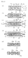
- Figs. 1 shows views showing a process for a method of manufacturing a multilayer wiring board according to a first embodiment of the present invention.
- the method of manufacturing a multilayer wiring board according to the present invention includes the step of impregnating a raw material composition in a thermosetting resin in a porous laminated product 30 including two or more porous layers 11 and a wiring layer 20 provided between the porous layers 11 and formed in any of the porous layers 11 and step of half curing or curing them.
- the porous laminated product 30 includes two or more wiring layers 20 and a pattern portion 21 of the wiring layer can be conductively connected between the layers through a conductor 32 in a through hole 11a provided on the porous layer 11.
- a lamination unit U comprises the porous layer 11 having the plurality of through holes 11a, the wiring layer 20 formed on at least one of surfaces of the porous layer 11, and the conductor 32 erected in the through hole 11a from the pattern portion 21 of the wiring layer 20.
- the lamination unit U In order to fabricate the lamination unit U, as shown in Figs. 2, it is preferable to comprise the step of providing and attaching by a wet coagulating method, the porous layer 11 formed of a resin on a metal foil 10 having a conductive bump 2a which is almost equal hight on the side surface of film formation, and the step of etching a metal foil 1 of the metal foil 10 having a bump, thereby forming the pattern portion 21 of the wiring layer 20.
- Example of the method of forming the metal foil 10 having a bump include a forming method using etching as shown in Figs . 2, a forming method using plating, a forming method using a conductive paste and the like.
- ametal laminatedplate comprising two kinds of metal layers 1 and 2 is first prepared.
- One of the metal layers 1 and 2 constituting the metal laminated plate may become the wiring layer and the other may become the conductive bump 2a. Therefore, a metal is selected corresponding to each material.
- copper, cupro-nickel, bronze, brass, aluminum, nickel, iron, stainless, gold, silver, platinum and the like can be used. It is preferable that these metal layers 1 and 2 should have thicknesses of 1 to 50 ⁇ m. It is preferable that a surface on the film formation side of the metal layer 1 should be subjected to various physical or chemical surfacing processes such as a rough surfacing process or a blacking process in order to enhance an adhesion to the porous layer 11.
- the metal layer 1 to be the wiring layer should be formed of copper in respect of an adhesion to the resin porous layer 11 formed by the wet coagulating method, the workability of the wiring pattern and the like.
- a metal which can be selectively etched during the etching without corroding the metal layer 1 is selected for the metal layer 2. More specifically, aluminum or the like can be used. A cladding material, a plating material and the like can be used for the metal laminated plate.
- a mask layer 3 for resisting the etching is formed in a portion on the surface of the metal layer 2 on which the conductive bump 2a is to be formed.
- Screen printing or photolithography can be utilized for forming the mask layer 3.
- the size of each mask layer 3 is determined by the area of the upper surface of the conductive bump 2a and can have a diameter of 5 to 500 ⁇ m.
- the shape of the upper surface of the conductive bump 2a can be controlled by the shape of each mask layer 3 and can be a circle, a square, a shape formed in conformity with a wiring pattern and the like.
- the metal layer 2 is etched to form the conductive bump 2a.
- etching conditions are adjusted to prevent excessive undercutting.
- the etching is preferably carried out by using an etchant for selectively etching the metal layer 2.
- the mask layer 3 is removed.
- removal using chemicals or separating removal is preferably carried out. Consequently, it is possible to form the metal foil 10 having the conductive bump 2a which is almost equal hight on the side surface of film formation.
- the resin porous layer 11 is formed and attached by the wet coagulating method utilizing the metal foil 10 having the bump described above.
- the amount of a film formation solution 4 should be applied such regulation that the surface of the resin porous layer 11 is almost on a level with the conductive bump 2a after the film formation.
- the porous layer 11 should have a vacancy rate of 30 to 90% and a mean pore size of 0.1 to 10 ⁇ m.
- a resin having an excellent heat resistance and a high mechanical strength is preferable for the material of the porous layer 11 to be used in the present invention, and it is possible to employ various resins such as polyimide, polyester, polyamide, particularly, aromatic polyamide, polyamideimide, polyetherimide, polyether sulfone and polyether ketone.
- various resins such as polyimide, polyester, polyamide, particularly, aromatic polyamide, polyamideimide, polyetherimide, polyether sulfone and polyether ketone.
- a polyimide based resin is preferable because of an excellent insulating property and heat resistance and an excellent adhesion with a metal layer.
- the aromatic polyamide is preferable because of an excellent insulating property and heat resistance and a lower coefficient of thermal linear expansion.
- a film forming solution (dope) having a resin and an additive dissolved in a solvent is prepared and is applied (cast) to a film forming base material, and is then immersed in a coagulating solution to carry out solvent substitution. Consequently, the resin is coagulated (changed into a gel) and the coagulating solution is then dried and removed. Thus, the porous layer can be obtained.
- the polyamide based resin mainly including a repetition unit in which an acid residue and an amine residue is imide bonded may contain other copolymerized components andblended compounds.
- polyimide having an aromatic group as a main chain for example, polyimide composed of a polymerized product containing a tetracarboxylic acid component and an aromatic diamine component can be employed.
- a polymer having a limiting viscosity of 0.55 to 3.00, preferably, 0.60 to 0.85 (a measured value at 30 °C) can be used.
- the polymer having the limiting viscosity within the above range can be formed into a porous film having an excellent dissolving property in a solvent, a great mechanical strength and independence.
- a polymer or a precursor thereof can be used for film formation.
- the polyamide acid has an advantage that a molecular structure is less restricted because it has a more excellent dissolving property as compared with polyimide. While the polymer may be completely changed into imide, 70 % or more of a change rate to imide is permitted. In the case in which a polymer having a comparatively high change rate to imide is used for doping, it is preferable to use a polymer including, in a repetition unit, a component having a high flexibility such as butanetetradicarboxylic anhydride.
- Any solvent for dissolving the polyimide based resin or the precursor thereof can be used. It is preferable to use an aprotic polar solvent such as N-methyl-2-pyrrolidone, N,N-dimethylacetamide, N,N-dimethylformamide or dimethylsulfoxide in respect of a dissolving property and a solvent substitution speed for a coagulating solvent in the case in which a porous film is formed by the wet coagulation process.
- Preferable examples include N-methyl-2-pyrrolidone.
- a solvent such as diethylene glycol, dimethyl ether or diethyleneglycol diethylether may be mixed to regulate the speed of a solvent substitution in the wet coagulation process.
- the aromatic polyamide includes so-called para type aramid and metha type aramid, and those in which apart of their main chain is substituted by diphenyl ether, diphenyl propane, diphenyl methane, diphenyl ketone, diphenyl sulfoxide or those in which biphenyl or a hydrogen group of an aromatic ring is substituted by a methyl group, a halogen atom or the like.
- para type aramid examples include poly p-phenyleneterephthalamide.
- the aramid thus constituted by only a rigid component is to be dissolved in a special reagent.
- aromatic polyamide used for the porous layer accordingly, it is preferable to at least partially use aramid having a part of main chain substituted by a component having a flexibility or the metha type aramid.
- Examples of the component giving a flexibility include m-phenylene, 2,7-naphthalene, diphenyl ether, 2,2-diphenyl propane and diphenyl methane.
- Such component is used as a dicarboxylic monomer or a diamine monomer for copolymerization and is thus introduced into a bone structure.
- the component having a higher copolymerization ratio generally has a more excellent dissolving property for a solvent.
- Examples of the solvent for dissolving the aromatic polyamide include tetramethyl urea, hexamethyl phospholamide, N,N-dimethyl acetamide, N-methyl-2-pyrrolidone, N-methylpiperidone-2, N,N-dimethylethylene urea, N,N,N',N'-tetramethyl allonic amide, N-methyl caprolactam, N-acethyl pyrrolidine, N,N-diethyl acetamide, N-ethyl pyrrolidone-2, N,N-dimethyl propionic amide, N,N-dimethyl isobutyl amide, N-methyl formamide, N,N-dimethyl propylene urea and their mixed systems.
- an aprotic polar solvent such as N-methyl-2-pyrrolidone, N,N-dimethyl acetamide or N,N-dimethyl formamide in respect of a dissolving property and a solvent substitution speed for a coagulating solvent. More preferable examples include N-methyl-2-pyrrolidone.
- a solvent such as diethyleneglycol dimethy ether or diethyleneglycol diethyl ether or diethyleneglycol dibutyl ether may be mixed to regulate the speed of a solvent substitution.
- the dope in the wet coagulation process is applied at a temperature of -20 to 40°C.
- any coagulating solution which does not dissolve a resin to be used and has a compatibility with the solvent.
- the coagulating solution water, alcohols such as methanol, ethanol and isopropyl alcohol and their mixed solution can be used, particularly, the water can be used suitably.
- the temperature of the coagulating solution at time of immersion is not particularly restricted but a temperature of 0 to 90 °C is preferable.
- the polymer concentration of a film forming solution preferably ranges from 5 % by weight to 25 % by weight, more preferably, 7 % by weight to 20 % by weight. If the concentration is too high, a viscosity is excessively increased and handling is hard to perform. If the concentration is too low, a porous film tends to be formed with difficulty.
- an inorganic material such as lithium nitrate or an organic material such as polyvinyl pyrrolidone can also be added. It is preferable that the concentration of an additive should be 1 % by weight to 10 % by weight in a solution. If the lithium nitrate is added, the substitution speed of a solvent and a coagulating solution is increased and a finger void structure (a structure having a finger-like void) is formed in a sponge structure. When an additive for reducing a coagulation speed such as polyvinyl pyrrolidone is added, it is possible to obtain a porous layer having a sponge structure expanded uniformly.
- the dope is applied to have a constant thickness and is immersed in a coagulating solution such as water and is thus coagulated or is left in a water vapor atmosphere and is thus coagulated and is then immersed in the water.
- a coagulating solution such as water and is thus coagulated or is left in a water vapor atmosphere and is thus coagulated and is then immersed in the water.
- the solvent is removed so that a porous film is formed.
- a drying temperature is not particularly limited but is desirably 200 °C or less.
- an upper surface 2b of the conductive bump 2a should be exposed from the porous layer 11 after the film formation as shown in Fig. 2(f).
- This can be achieved by regulating a coating thickness t.
- the thickness of the porous layer obtained may be slightly lowered than the conductive bump by the contraction of the film.
- a method carrying out a surfacing process over the upper surface of the conductive bump there is also used.
- the porous layer is formed of a polyimide based resin by using a precursor (ie.polyamide acid), a heat treatment is finally carried out at 200 to 500 °C to heat and ring-close the precursor.
- a precursor ie.polyamide acid
- the pattern portion 21 is formed against the metal layer 1 by etching using an etchant, thereby constituting the wiring layer 20.
- an etchant corresponding to the type of the metal can be used.
- a dry film resist or the like can be used.
- the lamination unit U thus obtained is provided as shown in Fig. 1(b), and constitutes a porous laminated product 30.
- the lamination unit U it is preferable that positioning should be carried out by using a guide pin or the like.
- the porous laminated product 30 includes two or more wiring layers 20 and the pattern portion 21 of the wiring layer 20 is conductively connected between the layers through the conductor 32 in the through hole 11a provided on the porous layer 11.
- a solder coating layer may be formed by separately performing solder plating over the surface of the conductor 32. It is preferable that the mask layer 3 shown in Fig. 2(b) should be subjected to solder pattern plating or the like and should be used without removal.
- the porous laminatedproduct 30 is impregnated with a rawmaterial composition R of a thermosetting resin and is half cured or cured.
- the raw material composition R is impregnated and half cured to prepare a half cured product 31, and a metal foil 25 is further provided thereon. Then, heating and pressurization are carried out to cure the half cured product 31 and bond a metal foil 25 thereto (see Fig. 1(d)).
- Examples of a method of impregnating the raw material composition R of the thermosetting resin include a method of supporting the porous laminated product 30 on a support plate 40 having a flat surface on one surface side and directly coating the surface of the porous laminated product 30 with the raw material composition R of the thermosetting resin by various coaters or the like, and a method of laminating a solid coating film obtained by coating and drying the raw material composition R on the surface of a base material sheet and impregnating them by heating and pressurization.
- the raw material composition R may be impregnated and half cured or cured in the same manner as in injection molding or transfer molding for the thermosetting resin.
- the area of a non-pattern portion is equal to or larger than a half of the whole surface. Therefore, it is possible to easily impregnate the raw material composition R from the surface. Also in the case in which the metal foil on the most surface or the like is not patterned, the raw material composition R can be impregnated from the peripheral edge portion of the porous laminated product 30.
- thermosetting resin includes an epoxy resin, a phenol resin, a polyimide resin, polyamide acid and the like, and the epoxy resin, a mixture of the epoxy resin and other resins and the like are preferable in respect of cost and easy handling.
- the raw material composition of the thermosetting resin may contain a catalyst, a curing agent, a flame retardant, a filler, aplasticizer, an accelerator and the like in addition to a solvent.
- the solvent contained in a raw material solution for the thermosetting resin include ketones, acetate esters, ethers, aromatic hydrocarbons, alcohols and the like.
- the well-known conditions corresponding to the type of a resin or the like are preferably set to the half curing conditions. It is preferable that the porous laminated product 30 should be pressurized on such a condition that the raw material composition R does not enter the contact surface between the surface of the pattern portion 21 and the conductor 32 in the porous laminated product 30.
- specific pressurizing conditions 0.1 to 100 MPa is preferable and 0.5 to 50 MPa is more preferable.
- a metal foil 25 is further provided on the half cured product 31 and the half cured product 31 is cured to bond the metal foil 25 by heating and pressurization.
- the curing conditions may be set depending on the type of the resin or the like.
- the metal foil 25 should be patterned by etching using an etchant or the like. Consequently, it is possible to manufacture a multilayer wiring board having four layers with an interlayer connecting structure. According to the present embodiment, it is possible to manufacture a multilayer wiring board having the number of lamination units U and one layer by a simple method.
- the multilayer wiring board of the present invention has such a lamination structure that the porous layer 11 having two or more layers and the wiring layer 20 provided between the porous layers 11 and formed on any of the porous layers 11 are integrated by a thermosetting resin which is impregnated and cured. Moreover, it is preferable that the lamination structure should have two or more wiring layers 20 and the pattern portion 21 of the wiring layer 20 should be conductively connected between the layers through the conductor 32 in the through hole 11a provided on the porous layer 11.
- the metal foil 10 having a bump is formed by the etching.
- the following method can be employed. More specifically, as shown in Figs. 3(a) to 3(d), a dry film resist 7 is first provided on a metal layer 1 and is exposed and developed to form an opening 7a. By carrying out electrolytic plating or the like over that portion, then, a conductive bump 2a can be formed. Thereafter, it is preferable that the dry film resist 7 shouldbe removedby using chemicals orbe removed by a separation. According to such a method, the conductive bump 2a and the metal layer 1 can be formed of the same metal. In the case in which the hight of the conductive bump 2a is nonuniform, it can become uniform by cutting, polishing or the like.
- the conductive bump 2a is to be formed of a conductive paste
- the conductive paste should be printed in a predetermined portion by a printing method such as screen printing.
- the printing may be carried out separately several times in order to cause a thickness to be constant or more.
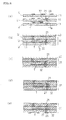
- Figs. 4 are views showing a process for a method of manufacturing a multilayer wiring board according to a second embodiment of the present invention.
- a raw material composition R of a thermosetting resin is previously impregnated and cured in a porous laminated product 30, and a conductive connecting structure between wiring layers is then formed.
- the raw material composition of a thermosetting resin is impregnated and cured in the porous laminated product 30 by using a lamination unit U including a porous layer 11 having no through hole and a wiring layer 20 formed on at least one of the surfaces of the porous layer 11 in the same manner as in the first embodiment.
- a through hole 36 penetrating through a whole cured product 35 is formed by drilling or the like.
- a diameter increasing portion 21a (pad) having the diameter of a pattern increased should be formed and a hole should be opened to be a through hole 36 to penetrate through the diameter increasing portion 21a in order to enhance the reliability of the interlayer connection.
- a plated layer 37 is formed by nonelectrolytic plating, electrolytic plating or the like. It is preferable that the electrolytic plating should be carried out by using the nonelectrolytic plated layer as a plating electrode after the nonelectrolytic plating is carried out.
- the plated layer 37 includes both surface portions 37b and 37c and a through hole plated portion 37a provided on the internal surface of the through hole 36.
- pattern portions 37d and 37e are formed by etching or the like. In that case, it is preferable that an etching resist should be provided in an opening portion such that the through hole plated portion 37a is not etched.
- the through hole plated portion 37a can conductively connect the wiring layers provided on both surfaces and can conductively connect the intermediate wiring layer.
- a metal foil may be provided and bonded to both surfaces and a through hole 36 may be formed thereon by drilling or the like to be subjected to through hole plating.
- Figs. 5 are views showing a process for a method of manufacturing a multilayer wiring board according to a third embodiment of the present invention.
- a raw material composition R is impregnated from the peripheral edge portion of a porous laminated product 30 by using a lamination unit U1 having a metal foil 22 which is not patterned.
- a lamination unit U1 comprising a porous layer 11 having a plurality of through holes 11a, a metal foil 22 formed on one of the surfaces of the porous layer 11 and a through hole plating 32a formed in the through hole 11a
- a lamination unit U2 comprising a porous layer 11 having a plurality of through holes 11a, a wiring layer 20 formed on both surfaces of the porous layer 11, and a through hole 32a formed in the through hole 11a.
- the lamination unit U1 can be fabricated in the following manner, for example.
- the laser irradiation condition is adjusted so that the surface of the through hole 11a is coated with melted layer.
- nonelectrolytic plating is carried out with other portions resisted. Consequently, it is possible to fabricate the lamination unit U1 including the through hole plating 32a having a comparatively uniform thickness.
- the lamination unit U2 can be fabricated in the following manner, for example.
- the laser irradiation condition is adjusted so that the surface of the through hole 11a is coated with melted layer.
- the porous laminated product 30 having the above lamination units is interposed between two guiding sheets 41.
- the guiding sheet 41 can prevent the raw material composition R of a thermosetting resin from going around both surfaces of the porous laminated product 30. While a sheet formed of a heat-resistant resin which is resistant to heating can be used for the guiding sheet 41, it is preferable that a heat-resistant adhesive layer such as a silicone based adhesive should be provided on a surface of the guiding sheet 41 in order to reliably prevent the raw material composition R from going around.
- the raw material composition R of a thermosetting resin is compressed and injected in this state and is thus impregnated in the porous laminated product 30.
- the heating temperature of the metal mold 42 may be set to obtain a sufficient fluidity and so as not to cure the raw material composition R.
- the heating temperature of the metal mold 42 may be set to sufficiently cure the impregnated raw material composition R.
- the pressing is released to take out the cured product and the metal foil 22 is subjected to pattern etching, thereby forming a pattern portion 22a for the wiring layers provided on both surfaces.
- Figs. 6 are views showing a process for a method of manufacturing a multilayer wiring board according to a fourth embodiment of the present invention.
- the porous laminated product 30 set in a state in which a passive component T is provided between porous layers 11 and can be conductively connected to a wiring layer 20 or in a conductive connecting state.
- the present embodiment is effective in the case where the thickness of the passive component T is less than the thickness of the adjacent porous layer 11. Only different portions from the above-mentioned embodiments will be described below.
- the passive component T is provided such that a terminal portion (an electrode portion) of the passive component T can be conductively connected to a pattern portion 21 of a wiring layer 20 in a lamination unit U.
- the terminal portion of the passive component T is bonded to the pattern portion 21 by reflow soldering such that both of them are brought into a conductive connecting state.
- any of a resistor, a capacitor, a coil and the like is used for the passive component T and these may be formed into an array, a network or the like.
- an active component such as a semiconductor circuit (for example, a bare chip) or a transistor and an element constituting the passive component T and the like.
- an element constituting the resistor is formed by printing a carbon containing resin or the like.
- an element constituting the capacitor forms a predetermined capacity between patterns (a material having a high dielectric constant may be used together if necessary).
- Examples of an element constituting a coil include a spiral wiring pattern.
- a semiconductor chip may be sealed and a bare chip or the like is preferable.
- the porous laminated product 30 of the lamination unit U is formed.
- the porous layer 11 to be pressed in contact with the passive component T is deformed and a space for providing the passive component T can easily be maintained.
- the impregnating property of the raw material composition of a thermosetting resin is slightly reduced in some cases. However, insulating functions are not deteriorated at all.
- the raw material composition of a thermosetting resin is impregnated and cured in the porous laminated product 30.
- Figs. 7 are views showing a process for a method of manufacturing a multilayer wiring board according to a fifth embodiment of the present invention.
- the porous laminated product 30 set in a state in which a passive component T is provided in an opening 11b of a porous layer 11 and can be conductively connected to a wiring layer 20 or in a conductive connecting state.
- the present embodiment is effective in the case in which the thickness of the passive component T is more than that of the adjacent porous layer 11. Only different portions from the above-mentioned embodiments will be described below.
- the passive component T is provided such that a terminal portion (an electrode portion) of the passive component T can be conductively connected to a pattern portion 21 of a wiring layer 20 in a lamination unit U and an opening portion 11b of the porous layer 11 is provided in such a position that the passive component T to be arranged can be inserted.
- the terminal portion of the passive component T is bonded to the pattern portion 21 through reflow soldering such that both of them are brought into a conductive connecting state.
- the shape and size of the opening portion 11b may be the same as or slightly different from the outer periphery of the passive component T. In the case in which the passive component T is not connected, the opening portion 11b can also have the function of positioning the passive component T. In that case, it is preferable that the shape and size of the opening portion 11b can hold the outer periphery of the passive component T.
- any of a resistor, a capacitor, a coil and the like is used for the passive component T and these may be formed into an array, a network or the like.
- an active component such as a semiconductor circuit (for example, a bare chip) or a transistor and an element constituting the passive component T and the like.
- an element constituting the resistor is formed by printing a carbon containing resin or the like.
- an element constituting the capacitor forms a predetermined capacity between patterns (a material having a high dielectric constant may be used together if necessary).
- Examples of an element constituting a coil include a spiral wiring pattern.
- a semiconductor chip may be sealed and a bare chip or the like is preferable.
- the porous laminated product 30 of the lamination unit U is formed.
- the porous layer 11 to be pressed in contact with the passive component T is deformed and a space for providing the passive component T can easily be maintained.
- the impregnating property of the raw material composition of a thermosetting resin is slightly reduced in some cases. However, insulating functions are not deteriorated at all.
- the raw material composition of a thermosetting resin is impregnated and cured in the porous laminated product 30.
- At least one of the passive component T, the active component and the element constituting them is provided in the opening portion 11b of the porous layer 11 and is conductively connected to the wiring layer 20.
- Vacancy rate (%) ⁇ 1 - ((weight / density)/volume) ⁇ ⁇ 100
- the volume and weight of the porous layer were measured to calculate the vacancy rate by the above-mentioned equation using the density of a material.
- a pattern was formed on a copper foil having a weight of 1 ounce and a metal foil having a bump was thus prepared by etching (half etching) .
- the hight of the bump was 20 ⁇ m and the diameter of the bump was 150 ⁇ m.
- a film formation solution comprising 19 parts by weight (molar ratio of 100 : 15 : 85) of BPDA (biphenyltetracarboxylic acid dianhydrate) - DDE (diaminodiphenylether) - PPD (paraphenylene diamine) based polyimide precursor and 81 parts by weight of N-methyl-2-pyrrolidone (NMP) was applied in a uniform thickness at a gap of 100 ⁇ m onto the surface of the metal foil having a bump by using a film applicator. Immediately after the application, the applied surface was immersed in pure water at 25°C and a polyimide precursor was thus coagulated. After the coagulation, drying was carried out for one hour or more at 90°C.
- BPDA biphenyltetracarboxylic acid dianhydrate
- DDE diaminodiphenylether
- PPD paraphenylene diamine
- NMP N-methyl-2-pyrrolidone
- the polyimide porous layer had a thickness of 18 ⁇ m and a sponge structure, and had a whole vacancy rate of 50% and a mean pore size of 0.2 ⁇ m. Moreover, the upper surface of the conductive bump was wholly exposed.
- the copper foil laminated plate By using the metal foil laminated plate, the copper foil was subjected to etching by an etchant, thereby forming a wiring pattern. The pattern formation was excellent.
- Aromatic polyamide (CORNEX produced by Teijin Limited) was dissolved in N-methyl-2-pyrrolidone (NMP) , and furthermore, polyvinyl pyrrolidone (PVP) (K-90 produced by ISP Japan Co., Ltd.) and water were added thereto. Consequently, a polymer solution containing aromatic polyamide (9 parts by weight) , NMP (83 parts by weight) , PVP (4 parts by weight) and water (4 parts by weight) were obtained. The polymer solution was applied in a uniform thickness at a gap of 60 ⁇ m onto the surface of the metal foil having a bump by using a film applicator. Immediately after the application, the applied surface was immersed in a water tank at 60°C to form a porous layer.
- NMP N-methyl-2-pyrrolidone
- PVP polyvinyl pyrrolidone
- K-90 produced by ISP Japan Co., Ltd.
- the porous layer was preserved in the water for 24 hours and the solvent was removed therefrom. Thereafter, drying was carried out for one hour or more at 90°C.
- the porous layer had a thickness of approximately 10 ⁇ m and a sponge structure, and had a whole vacancy rate of approximately 50% and a mean pore size of 0.2 ⁇ m. Moreover, the upper surface of the conductive bump was wholly exposed.
- the copper foil laminated plate By using the metal foil laminated plate, the copper foil was subjected to etching by an etchant, thereby forming a wiring pattern. The pattern formation was excellent.
Landscapes
- Engineering & Computer Science (AREA)
- Manufacturing & Machinery (AREA)
- Microelectronics & Electronic Packaging (AREA)
- Production Of Multi-Layered Print Wiring Board (AREA)
- Printing Elements For Providing Electric Connections Between Printed Circuits (AREA)
- Laminated Bodies (AREA)
Abstract
Description
Claims (11)
- A method of manufacturing a multilayer wiring board comprising the steps of impregnating a raw material composition (R) of a thermosetting resin in a porous laminated product (30) including two or more porous layers (11) and a wiring layer (20) provided between the porous layers (11) and formed on any of the porous layers (11), and of half curing or curing the raw material composition (R).
- The method of manufacturing a multilayer wiring board according to claim 1, wherein the porous laminated product (30) includes two or more wiring layers (20) and is set in a state in which a pattern portion of the wiring layer (20) can be conductively connected between the wiring layers through a conductor (32) in a through hole (11a) provided in the porous layer (11) or in a conductive connecting state.
- The method of manufacturing a multilayer wiring board according to claim 1 or 2, wherein the porous laminated product (30) comprises a lamination unit (U) including a porous layer (11) having a plurality of through holes (11a), a wiring layer (20) formed on at least one of surfaces of the porous layer (11), and a conductor (32) erected in the through hole (11a) from the pattern portion (21) of the wiring layer (20).
- The method of manufacturing a multilayer wiring board according to claim 3, further comprising the step of using a metal foil (10) including a conductive bump (2a) having an almost equal hight on a film forming side surface to form and attach a resin porous layer (11) onto the metal foil (10) by a wet coagulating method and the step of etching the metal foil (10) to form a pattern portion (21) of the wiring layer to obtain the lamination unit.
- The method of manufacturing a multilayer wiring board according to claim 1 or 2, wherein the porous laminated product (30) is set in a state in which at least one of a passive component (T), an active component and an element constituting them is interposed between the porous layers (11) and can be conductively connected to the wiring layer (20) or in a conductive connecting state.
- The method of manufacturing a multilayer wiring board according to claim 1 or 2, wherein the porous laminated product is set in a state in which at least one of a passive component (T), an active component and an element constituting them is provided in an opening portion (11b) of the porous layer (11) and can be conductively connected to the wiring layer (20) or a conductive connecting state.
- A multilayer wiring board having such a lamination structure that two or more porous layers (11) and a wiring layer (20) provided between the porous layers (11) and formed on any of the porous layers (11) are integrated through an impregnated and cured thermosetting resin.
- The multilayer wiring board according to claim 7, wherein in the lamination structure, two or more wiring layers (20) are provided and a pattern portion (21) of the wiring layer (20) is conductively connected between the layers by a conductor (32) in a through hole (11a) provided in the porous layer (11).
- The multilayer wiring board according to claim 7 or 8, wherein in the lamination structure, at least one of a passive component (T) , an active component and an element constituting them is interposed between the porous layers (11) and is conductively connected to the wiring layer (20).
- The multilayer wiring board according to claim 7 or 8, wherein in the lamination structure, at least one of a passive component (T) , an active component and an element constituting them is provided in an opening portion (11a) of the porous layers (11) and is conductively connected to the wiring layer (20).
- The multilayer wiring board according to any one of claims 7 to 10, wherein the porous layer (11) is formed of polyimide or aromatic polyamide.
Applications Claiming Priority (4)
| Application Number | Priority Date | Filing Date | Title |
|---|---|---|---|
| JP2001183318 | 2001-06-18 | ||
| JP2001183318 | 2001-06-18 | ||
| JP2002003067A JP2003078244A (en) | 2001-06-18 | 2002-01-10 | Multilayer wiring board and manufacturing method thereof |
| JP2002003067 | 2002-01-10 |
Publications (2)
| Publication Number | Publication Date |
|---|---|
| EP1272022A2 true EP1272022A2 (en) | 2003-01-02 |
| EP1272022A3 EP1272022A3 (en) | 2004-09-01 |
Family
ID=26617101
Family Applications (1)
| Application Number | Title | Priority Date | Filing Date |
|---|---|---|---|
| EP02013457A Withdrawn EP1272022A3 (en) | 2001-06-18 | 2002-06-13 | Multilayer wiring board and method of manufacturing the same |
Country Status (4)
| Country | Link |
|---|---|
| US (1) | US7017264B2 (en) |
| EP (1) | EP1272022A3 (en) |
| JP (1) | JP2003078244A (en) |
| CN (1) | CN1276696C (en) |
Families Citing this family (11)
| Publication number | Priority date | Publication date | Assignee | Title |
|---|---|---|---|---|
| JP2004039897A (en) * | 2002-07-04 | 2004-02-05 | Toshiba Corp | How to connect electronic devices |
| WO2005078796A1 (en) | 2004-02-13 | 2005-08-25 | Murata Manufacturing Co., Ltd. | Electronic component and method for manufacturing the same |
| US9985207B2 (en) * | 2004-12-06 | 2018-05-29 | Flexenable Limited | Electronic devices |
| JP4819033B2 (en) * | 2005-01-27 | 2011-11-16 | パナソニック株式会社 | Multilayer circuit board manufacturing method |
| JP4276195B2 (en) * | 2005-03-04 | 2009-06-10 | Tdk株式会社 | Substrate storage method and coil component manufacturing method |
| JP2008085310A (en) * | 2006-08-28 | 2008-04-10 | Clover Denshi Kogyo Kk | Multilayer printed circuit board |
| US20080053688A1 (en) * | 2006-09-01 | 2008-03-06 | Samsung Electro-Mechanics Co., Ltd. | Printed circuit board and method of manufacturing the same |
| JP2015088750A (en) * | 2013-10-28 | 2015-05-07 | サムソン エレクトロ−メカニックス カンパニーリミテッド. | Core substrate and method for manufacturing core substrate |
| US9666514B2 (en) * | 2015-04-14 | 2017-05-30 | Invensas Corporation | High performance compliant substrate |
| JP2020123633A (en) * | 2019-01-29 | 2020-08-13 | Dic株式会社 | Wiring structure manufacturing method |
| CN110355932B (en) * | 2019-06-21 | 2020-06-19 | 西安交通大学 | Preparation device and method of multilayer dielectric material |
Family Cites Families (10)
| Publication number | Priority date | Publication date | Assignee | Title |
|---|---|---|---|---|
| US3303078A (en) | 1962-05-18 | 1967-02-07 | David Wolf | Method of making electrical components |
| CA1011002A (en) | 1974-05-16 | 1977-05-24 | Minnesota Mining And Manufacturing Company | Method for making printed circultry |
| US5136123A (en) | 1987-07-17 | 1992-08-04 | Junkosha Co., Ltd. | Multilayer circuit board |
| JPH05299796A (en) | 1992-04-22 | 1993-11-12 | Hitachi Chem Co Ltd | Multi-layer printed wiring board adhesive sheet and metal clad laminated board using the sheet |
| JP3146712B2 (en) | 1993-01-12 | 2001-03-19 | 松下電器産業株式会社 | Double-sided printed circuit board and method of manufacturing the same |
| CA2115334A1 (en) | 1993-02-10 | 1994-08-11 | Isao Tomioka | Film forming solution, porous film obtained therefrom and coated material with the porous film |
| JP3677892B2 (en) | 1995-10-16 | 2005-08-03 | 住友化学株式会社 | Prepreg and manufacturing method thereof, printed circuit board and printed circuit laminate using the same |
| DE69631573T2 (en) | 1995-10-16 | 2004-12-16 | Sumitomo Chemical Co., Ltd. | Prepreg, process for its manufacture and printed circuit board substrate using the same |
| JP3889856B2 (en) * | 1997-06-30 | 2007-03-07 | 松下電器産業株式会社 | Method for manufacturing printed wiring board with protruding electrodes |
| JP2001127389A (en) | 1999-11-01 | 2001-05-11 | Matsushita Electric Ind Co Ltd | Circuit board insulating material, circuit board, and method of manufacturing circuit board |
-
2002
- 2002-01-10 JP JP2002003067A patent/JP2003078244A/en active Pending
- 2002-06-11 US US10/171,502 patent/US7017264B2/en not_active Expired - Fee Related
- 2002-06-13 EP EP02013457A patent/EP1272022A3/en not_active Withdrawn
- 2002-06-18 CN CN02122643.1A patent/CN1276696C/en not_active Expired - Fee Related
Also Published As
| Publication number | Publication date |
|---|---|
| US20020192870A1 (en) | 2002-12-19 |
| US7017264B2 (en) | 2006-03-28 |
| CN1276696C (en) | 2006-09-20 |
| JP2003078244A (en) | 2003-03-14 |
| EP1272022A3 (en) | 2004-09-01 |
| CN1392763A (en) | 2003-01-22 |
Similar Documents
| Publication | Publication Date | Title |
|---|---|---|
| US6807729B2 (en) | Method of manufacturing metal foil | |
| US7174632B2 (en) | Method of manufacturing a double-sided circuit board | |
| JP2587596B2 (en) | Circuit board connecting material and method for manufacturing multilayer circuit board using the same | |
| KR19990013967A (en) | Wiring board and manufacturing method thereof | |
| WO2001045478A1 (en) | Multilayered printed wiring board and production method therefor | |
| US7017264B2 (en) | Method of manufacturing multilayer wiring board | |
| US6528733B2 (en) | Multi-layer circuit board and method of manufacturing same | |
| US7121000B2 (en) | Method for manufacturing multilayer wiring board | |
| US6761790B2 (en) | Wiring board and method of manufacturing the same | |
| US6759082B2 (en) | Metal foil laminated plate and method of manufacturing the same | |
| US7237332B2 (en) | Method of manufacturing wiring board | |
| JP2005116660A (en) | Conductive paste-filled substrate and manufacturing method thereof | |
| JP2003008233A (en) | Multilayer wiring board | |
| JP2003208820A (en) | Anisotropic conductive film and method for producing the same | |
| JP2004066763A (en) | Metal foil laminate and manufacturing method thereof | |
| JP2006306977A (en) | Composite, prepreg, metal foil-clad laminate, printed wiring board, multilayer printed wiring board, and methods for producing them | |
| JP2002344114A (en) | Wiring board and manufacturing method thereof | |
| JP2002208781A (en) | Wiring board prepreg and method of manufacturing the same | |
| JP2001094256A (en) | Multilayer printed wiring board and method of manufacturing the same | |
| JP2004066764A (en) | Metal foil laminate and manufacturing method thereof | |
| JPH10235795A (en) | Metal foil with insulating layer | |
| JP2003218160A (en) | Insulating film and multilayer wiring board using the same | |
| JP2005072398A (en) | Multilayer wiring board | |
| JP2004235265A (en) | Insulating film and multilayer wiring board using the same | |
| JP2004055405A (en) | Insulating film and multilayer wiring board using the same |
Legal Events
| Date | Code | Title | Description |
|---|---|---|---|
| PUAI | Public reference made under article 153(3) epc to a published international application that has entered the european phase |
Free format text: ORIGINAL CODE: 0009012 |
|
| AK | Designated contracting states |
Kind code of ref document: A2 Designated state(s): AT BE CH CY DE DK ES FI FR GB GR IE IT LI LU MC NL PT SE TR |
|
| AX | Request for extension of the european patent |
Free format text: AL;LT;LV;MK;RO;SI |
|
| PUAL | Search report despatched |
Free format text: ORIGINAL CODE: 0009013 |
|
| AK | Designated contracting states |
Kind code of ref document: A3 Designated state(s): AT BE CH CY DE DK ES FI FR GB GR IE IT LI LU MC NL PT SE TR |
|
| AX | Request for extension of the european patent |
Extension state: AL LT LV MK RO SI |
|
| STAA | Information on the status of an ep patent application or granted ep patent |
Free format text: STATUS: THE APPLICATION HAS BEEN WITHDRAWN |
|
| 18W | Application withdrawn |
Effective date: 20050119 |