EP1271812A2 - Optical signal regenerator - Google Patents
Optical signal regenerator Download PDFInfo
- Publication number
- EP1271812A2 EP1271812A2 EP02008651A EP02008651A EP1271812A2 EP 1271812 A2 EP1271812 A2 EP 1271812A2 EP 02008651 A EP02008651 A EP 02008651A EP 02008651 A EP02008651 A EP 02008651A EP 1271812 A2 EP1271812 A2 EP 1271812A2
- Authority
- EP
- European Patent Office
- Prior art keywords
- optical
- clock
- signal
- regenerator
- splitter
- Prior art date
- Legal status (The legal status is an assumption and is not a legal conclusion. Google has not performed a legal analysis and makes no representation as to the accuracy of the status listed.)
- Withdrawn
Links
Images



Classifications
-
- H—ELECTRICITY
- H04—ELECTRIC COMMUNICATION TECHNIQUE
- H04B—TRANSMISSION
- H04B10/00—Transmission systems employing electromagnetic waves other than radio-waves, e.g. infrared, visible or ultraviolet light, or employing corpuscular radiation, e.g. quantum communication
- H04B10/29—Repeaters
- H04B10/291—Repeaters in which processing or amplification is carried out without conversion of the main signal from optical form
- H04B10/299—Signal waveform processing, e.g. reshaping or retiming
Definitions
- This invention relates to an optical signal regenerator to regenerate optical signals in an intact optical state.
- an optical clock pulse train synchronizing with an input optical signal pulse train is gated by the input optical signal pulse train. Owing to this operation, even if a pulse waveform of the input optical signal is distorted, each pulse waveform of output optical signals becomes almost identical to that of the optical clock pulse train.
- An optical signal regenerator comprises an optical splitter to split an input optical signal into n (an even number) portions, a clock generator to generate a clock having a 1/n frequency of a bit rate of the input optical signal out of the input optical signal, an optical clock generator to generate n optical clocks having same frequency as that of the clock from the clock generator and matching to each timing of n time slots of the input optical signal, according to the clock from the clock generator, n optical regenerators, each regenerating signal in an optical state according to both optical signal from the optical splitter and optical clock output from the optical clock generator, and an optical combiner to combine optical signals output from the n optical regenerators.
- FIG. 1 shows a schematic block diagram of a first embodiment according to the invention.
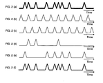
- FIGS. 2(a)-2(f) respectively shows a waveform of each part.
- FIG. 2(a) shows a waveform example of the optical pulse signal 10.
- X is set to 40.
- An optical splitter 14 applies about 1/10 of the optical power of the optical pulse signal 10 from the input terminal 12 to a clock recovery circuit 16 and the rest to an optical splitter 18.
- the optical splitter 18 splits the input light into half and applies one portion to an optical regenerator 20A and the other to an optical regenerator 20B.
- the clock recovery circuit 16 regenerates an electric clock signal of X/2 (GHz) out of the optical pulse from the optical splitter 14.
- Phase adjusters (delay circuits) 22A and 22B adjust phase of the electric clock signal from the clock recovery circuit 16 so that the phases of the outputs differ by ⁇ from each other and the phase of the optical signal accords with that of the optical clock at each of the optical regenerators 20A and 20B.
- Each of optical clock pulse generators 24A and 24B synchronizes with the output from the phase adjustor 22A, 22B, generates an optical clock of X/2 (GHz), and applies the clock to the optical regenerator 20A, 20B.
- FIGS. 2(b) and 2(c) respectively shows an optical clock waveform output from the optical clock generator 24A, 24B.
- the optical regenerators 20A, 20B are apparatuses to copy a bit pattern of the optical signal from the optical splitter 18 onto an optical clock entered separately and have both functions of optical waveform reshaping and jitter removing (retiming).
- FIGS. 2(d) and 2(e) respectively shows an optical signal waveform regenerated by the optical regenerator 20A, 20B.
- the optical regenerator 20A outputs an optical signal regenerated from one optical pulse signal of X/2 (Gbit/s) and the optical regenerator 24B outputs an optical signal regenerated from the other optical pulse signal of X/2 (Gbit/s). That is, in this embodiment, two regenerating systems to operate at half speed of the input optical pulse signal 10 are provided to separately regenerate optical signals whose bit locations shift reciprocally in the time domain. With this operation, a frequency of optical clocks needed for the optical regenerators 20A and 20B is sufficient with a half bit rate of the input optical pulse signal 10, and thus it becomes easy to stably generate the optical clocks.
- an optical delay unit 26 delays the light from the optical regenerator 20A by 1 bit period of X (Gbit/s), and a polarization controller 28A adjusts the light from the optical delay unit 26 to become a linear polarization in a predetermined polarization direction.
- a polarization controller 28B adjusts the light from the optical regenerator 20B to become a linear polarization in the predetermined polarization direction or a polarization direction orthogonal to the predetermined direction.
- a polarization composer namely, a polarizing beam splitter 30 combines the optical signals from the polarization controllers 28A and 28B in a mutually orthogonal polarization state.
- FIG. 2(f) shows a signal waveform output from the polarization composer 30.
- the light from the polarization composer 30 is output toward the outside from an output terminal 32.
- a bit pattern of the input optical signal 10 is exactly reproduced, a waveform of each pulse is reshaped, and jitter is removed. Since polarizations of temporally adjacent optical pulses are mutually orthogonalized, not only the improvement of transmission characteristics are expected but also the interference between the adjacent optical pulses is prevented even if they are partly overlapped. Accordingly, it is possible to widen the optical pulse width of the optical clocks generated by the optical clock pulse generators 24A and 24B, and thus the production of the optical clock pulse generators 24A and 24B becomes much easier.
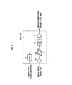
- FIG. 3 shows a schematic block diagram of the optical regenerator 20A and 20B.
- the optical signal from the optical splitter 18 is amplified by an optical amplifier 40 and enters an electroabsorption (EA) modulator 44 through ports A and B of an optical circulator 42.
- the optical clocks from the optical clock pulse generators 24A and 24B also enter the EA modulator 44 in the opposite direction to the optical signal.
- the EA modulator 44 functions as an optical gate to gate optical clocks according to whether or not an optical pulse exists in the optical signal. That is, the EA modulator 44 converts the optical clocks from the optical clock pulse generators 24A and 24B into optical pulse signals having the same bit pattern with that of the optical signal from the optical splitter 18.
- the detailed operation of the EA modulator 44 is explained in, for example, the U.S. Pat. No. 5,959,764, the entire contents of which are incorporated herein by reference.
- the optical clocks gated by the EA modulator 44 are applied to the optical delay unit 26 or the polarization controller 28B through ports B and C of the optical circulators 42, an optical filter 46, and an optical amplifier 48.
- the optical filter 46 is disposed so as to remove unnecessary wavelength components.
- FIG. 4 shows a schematic block diagram of such a modified embodiment. Identical elements are labeled with common reference numerals to those in FIG. 1.
- An optical splitter 34 splits the optical clock of X/2 (GHz) from the optical clock pulse generator 24A into two portions and applies one portion to the optical regenerator 20A and the other to the optical clock recovery circuit 20B through an optical delay unit 36.
- the optical delay unit 36 delays the optical clock from the optical clock pulse generator 24A having timing shown in FIG. 2(b) and generates an optical clock having timing shown in FIG. 2(c). Accordingly, similarly to the embodiment shown in FIG. 1, the optical regenerators 20A and 20B regenerate the two kinds of optical pulse signals of X/2 (Gbit/s) in an optical state and the regenerated optical signals are combined in an orthogonal polarization.
- One of merits in the embodiment shown in FIG. 4 is that it requires only one optical clock pulse generator 24A.
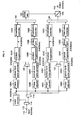
- FIG. 5 shows a schematic block diagram of such an embodiment.
- An optical pulse signal 110 of X enters an input terminal 112.
- An optical splitter 114 applies about 1/10 of the power of the optical pulse signal 110 from the input terminal 112 to a clock recovery circuit 116 and the rest to an optical splitter 118.
- the optical splitter 118 splits the input light into two portions of the same power and applies one portion to an optical splitter 120 and the other to an optical splitter 122.
- the optical splitter 120 splits the input light into two portions of the same power and applies one portion to an optical regenerator 124A and the other to an optical regenerator 124B.
- the optical splitter 122 splits the input light into two portions of the same power and applies one portion to an optical regenerator 124C and the other to an optical regenerator 124D.
- the input optical pulse signal 110 is divided into four time slot units in the time domain, and the optical regenerator 124A regenerates an optical pulse signal in a first slot in an optical state, the optical regenerator 124B regenerates an optical pulse signal in a third slot, the optical regenerator 124C regenerates an optical pulse signal in a second slot, and the optical regenerator 124D regenerates an optical pulse signal in a fourth slot.
- the clock recovery circuit 116 regenerates an electric clock signal of X/4 (GHz) out of the optical pulse from the optical splitter 114.
- the clock from the clock recovery circuit 116 is applied to optical clock pulse generators 128A, 128B, 128C, and 128D through phase adjusters 126A, 126B, 126C, and 126D.
- the phase adjusters (delay circuits) 126A, 126b, 126C, and 126D respectively delays the clock from the clock recovery circuit 116 so that optical clock from the optical clock pulse generators 128A, 128B, 128C, and 128D correspond to respective temporal timing of the above first time slot, third time slot, second time slot, and forth time slot.
- the optical clock pulse generators 128A, 128B, 128C, and 128D respectively synchronize with the clock from the phase adjusters 126A, 126b, 126C, and 126D to generate an optical clocks of X/4 (GHz) and apply them to the optical regenerators 124A, 124B, 124C, and 124D.
- Each of the optical regenerators 124A, 124B, 124C, and 124D has the same configuration as that of the optical regenerator 20A and 20B, reshapes a waveforms of the input optical signal, and removes jitter.
- the optical regenerators 124A and 124B respectively copies a bit pattern of the optical signal from the optical splitter 120 onto the optical clocks from the optical clock pulse generators 128A and 128B, and also the optical regenerators 124C and 124D respectively copies a bit pattern of the optical signal from the optical splitter 122 onto the optical clocks from the optical clock pulse generators 128C and 128D.
- the optical regenerator 124A regenerates the optical pulse signal in the first time slot of the input optical pulse signal 110
- the optical regenerator 124B regenerates the optical pulse signal in third time slot
- the optical regenerator 124C regenerates the optical pulse signal in the second time slot
- the optical regenerator 124D regenerates the optical pulse signal in the fourth time slot.
- the four optical regenerating systems that operate at a quarter speed of the input optical pulse signal 110 are provided and the optical signals in each of the four time slot units are regenerated separately.
- the frequency of the optical clock needed for the optical regenerators 124A, 124B, 124C, and 124D is sufficient with a quarter of the bit rate of the input optical pulse signal, and therefore it is easily generated in a stable condition.
- An optical delay unit 130B adjusts the timing of the light from the optical regenerator 124B to that of the third time slot so as to provide for combination with the regenerated optical signal in the first time slot.
- Polarization controllers 132A and 132B respectively controls polarizations of the light from the optical regenerator 124A and optical delay unit 130B so as to become linear polarizations in the same direction.
- An optical combiner 134 combines the light from the polarization controllers 132A and 132B. The optical combiner 134 functions as a time division multiplexer to multiplex the regenerated pulse signal in the first time slot and that in the third time slot of the time domain.
- the optical delay unit 130D adjusts the timing of the light from the optical regenerator 124D to that of the fourth time slot so as to provide for combination with the regenerated optical signal in the second time slot.
- the polarization controllers 132C and 132D respectively controls polarizations of the optical signals from the optical regenerator 124C and optical delay unit 130D so as to become linear polarizations in the same direction.
- An optical combiner 136 combines the optical signals from the polarization controllers 132C and 132D.
- the optical combiner 136 functions as a time division multiplexer to multiplex the regenerated optical pulse signal in the second time slot and that in the fourth time slot of the time domain.
- An optical delay unit 138 adjusts the timing of the light from the optical combiner 134 so as to provide for combination with the light from the optical combiner 136.
- a polarization combiner 140 combines the optical signals (the regenerated optical signals in the first and third time slots) from the optical delay unit 138 with those (the regenerated optical signals in the second and fourth time slots) from the optical combiner 136 in mutually orthogonal polarization.
- the regenerated optical signal of X (Gbit/s) combined by the polarization combiner 140 is output toward the outside through an output terminal 142.
- a waveform of the optical pulse is reshaped and jitter is removed by the optical regenerators 124A through 124D. Since polarizations of temporally adjacent optical pulses are mutually orthogonal, not only the improvement of transmission characteristics are expected but also the interference between the adjacent pulses does not occur even if they are partly overlapped. Accordingly, it is possible to widen the optical pulse width of the optical clocks generated by the optical clock pulse generators 128A through 128D, and thus the production of the optical clock pulse generators 128A through 128D becomes much easier.
- FIG. 6 A schematic block diagram of such a modified embodiment is shown in FIG. 6. Identical elements are labeled with common reference numerals to those in FIG. 5.
- An optical splitter 144 splits output light from the optical clock pulse generator 128A into four portions of the same power and applies to the optical regenerator 124A, and optical delay units 146, 148, and 150 respectively.
- the optical delay units 146, 148, and 150 respectively adjusts timing of the optical clock from the optical splitter 144 so as to match with that of the optical signal entered the optical regenerators 124B, 124C, and 124D and apply them to the optical regenerators 124B, 124C, and 124D.
Landscapes
- Physics & Mathematics (AREA)
- Electromagnetism (AREA)
- Engineering & Computer Science (AREA)
- Computer Networks & Wireless Communication (AREA)
- Signal Processing (AREA)
- Optical Communication System (AREA)
- Optical Modulation, Optical Deflection, Nonlinear Optics, Optical Demodulation, Optical Logic Elements (AREA)
Abstract
Description
Claims (4)
- An optical signal regenerator comprising:an optical splitter to split an input optical signal into n (an even number) portions;a clock generator to generate a clock having a 1/n frequency of a bit rate of the input optical signal out of the input optical signal;an optical clock generator to generate n optical clocks having a same frequency to that of the clock from the clock generator and matching to each timing of n time slots of the input optical signal according to the clock from the clock generator;n optical regenerators, each regenerating the signal in an intact optical state according to both optical signal from the optical splitter and optical clock from the optical clock generator; andan optical combiner to combine optical signals from the n optical regenerators.
- An optical signal regenerator of claim 1 wherein the optical combiner comprises n polarization controllers to control polarization of each optical signal from the n optical regenerators and a polarization combiner to combine the optical signals from the n polarization controllers so that adjacent time slots form orthogonal polarization.
- The optical signal regenerator of claim 1 or 2 wherein the optical clock generator compris es n phase adjuster s, each adjusting phase of the clock from the clock generator into a predetermined time slot within the n time slots of the input optics signal and n optical clock pulse generators to respectively generate optical clocks having same frequency according to the optical signals from the n phase adjusters.
- An optical signal regenerator wherein the optical clock generator comprises an optical clock pulse generator to generate an optical clock according to the clock from the clock generator, an optical clock splitter to split the optical clock from the optical clock pulse generator into n portions, and (n-1) optical delay units to control each timing of the optical clod from the optical clock splitter so as to become timing corresponding to a predetermined time slotwithin the n time slots of the input optical signal.
Applications Claiming Priority (2)
| Application Number | Priority Date | Filing Date | Title |
|---|---|---|---|
| JP2001184332 | 2001-06-19 | ||
| JP2001184332A JP2003005140A (en) | 2001-06-19 | 2001-06-19 | Optical signal reproduction device |
Publications (2)
| Publication Number | Publication Date |
|---|---|
| EP1271812A2 true EP1271812A2 (en) | 2003-01-02 |
| EP1271812A3 EP1271812A3 (en) | 2004-06-09 |
Family
ID=19024110
Family Applications (1)
| Application Number | Title | Priority Date | Filing Date |
|---|---|---|---|
| EP02008651A Withdrawn EP1271812A3 (en) | 2001-06-19 | 2002-04-17 | Optical signal regenerator |
Country Status (3)
| Country | Link |
|---|---|
| US (1) | US7116914B2 (en) |
| EP (1) | EP1271812A3 (en) |
| JP (1) | JP2003005140A (en) |
Cited By (2)
| Publication number | Priority date | Publication date | Assignee | Title |
|---|---|---|---|---|
| FR2879053A1 (en) * | 2005-03-24 | 2006-06-09 | France Telecom | Optical signal regenerator device for e.g. dense wavelength division multiplexing network, has modulator with surface processed in antireflecting manner to limit interactions between converted signal and pumping signal parasitic reflection |
| US7873284B2 (en) | 2004-04-22 | 2011-01-18 | Alcatel-Lucent Usa Inc. | Quadrature amplitude modulation of optical carriers |
Families Citing this family (6)
| Publication number | Priority date | Publication date | Assignee | Title |
|---|---|---|---|---|
| US20040042800A1 (en) * | 2002-08-30 | 2004-03-04 | Lawrence Brian L. | All-optical 3R regenerator using solitary wave interactions |
| ITMI20042312A1 (en) * | 2004-12-01 | 2005-03-01 | Marconi Comm Spa | MULTIPLEXER WITH OPTICAL ADD-DROP |
| US7590358B2 (en) * | 2005-02-28 | 2009-09-15 | Vladimir Grigoryan | Optical regenerative amplifier for binary phase shift-keying signals |
| US8213795B2 (en) * | 2007-05-09 | 2012-07-03 | University Of Central Florida Research Foundation, Inc. | Systems and methods of polarization time coding for optical communications |
| JP4705123B2 (en) * | 2008-03-14 | 2011-06-22 | 日本電信電話株式会社 | Quantum cryptographic key distribution system |
| US8644713B2 (en) * | 2009-11-12 | 2014-02-04 | Packet Photonics, Inc. | Optical burst mode clock and data recovery |
Family Cites Families (6)
| Publication number | Priority date | Publication date | Assignee | Title |
|---|---|---|---|---|
| JP3458613B2 (en) * | 1996-09-04 | 2003-10-20 | Kddi株式会社 | Wavelength conversion device and optical operation device |
| US6486990B1 (en) * | 1998-12-18 | 2002-11-26 | Nortel Networks Limited | Method and apparatus for communicating a clock signal in a soliton optical transmission system |
| US6607313B1 (en) * | 1999-06-23 | 2003-08-19 | Jds Fitel Inc. | Micro-optic delay element for use in a polarization multiplexed system |
| EP1076430A1 (en) * | 1999-07-23 | 2001-02-14 | BRITISH TELECOMMUNICATIONS public limited company | Optical regenerator for high-bitrate OTDM signals |
| FR2805417B1 (en) * | 2000-02-21 | 2002-05-31 | Cit Alcatel | REGENERATOR FOR WAVELENGTH MULTIPLEXING TRANSMISSION SYSTEM |
| WO2002067482A2 (en) * | 2001-02-16 | 2002-08-29 | Axe, Inc. | Receiver for high-speed optical signals |
-
2001
- 2001-06-19 JP JP2001184332A patent/JP2003005140A/en not_active Withdrawn
-
2002
- 2002-04-17 EP EP02008651A patent/EP1271812A3/en not_active Withdrawn
- 2002-06-12 US US10/170,138 patent/US7116914B2/en not_active Expired - Fee Related
Cited By (2)
| Publication number | Priority date | Publication date | Assignee | Title |
|---|---|---|---|---|
| US7873284B2 (en) | 2004-04-22 | 2011-01-18 | Alcatel-Lucent Usa Inc. | Quadrature amplitude modulation of optical carriers |
| FR2879053A1 (en) * | 2005-03-24 | 2006-06-09 | France Telecom | Optical signal regenerator device for e.g. dense wavelength division multiplexing network, has modulator with surface processed in antireflecting manner to limit interactions between converted signal and pumping signal parasitic reflection |
Also Published As
| Publication number | Publication date |
|---|---|
| US20020191259A1 (en) | 2002-12-19 |
| US7116914B2 (en) | 2006-10-03 |
| EP1271812A3 (en) | 2004-06-09 |
| JP2003005140A (en) | 2003-01-08 |
Similar Documents
| Publication | Publication Date | Title |
|---|---|---|
| US5786918A (en) | Optical communication system and optical transmitting device | |
| US20030175033A1 (en) | Optical transmission system, optical transmitter and methods thereof | |
| JP4105272B2 (en) | Optical regeneration method and apparatus for a system for optical fiber transmission of non-soliton signals | |
| JPH05268168A (en) | Optical signal transmission method | |
| GB2320634A (en) | Optical sampling by using an interferometer to modulate a pulse train | |
| US8705980B2 (en) | Optical modulation device and optical modulation method | |
| EP0924552A2 (en) | Opto-electronic frequency divider circuit and method of operating same | |
| US20020075536A1 (en) | Multi-wavelength all-optical regenerators ( mars) | |
| AU2003240411B2 (en) | Method and arrangement for reducing the signal degradation in an optical polarisation-multiplex signal | |
| US7116914B2 (en) | Optical signal regenerator | |
| JP3931670B2 (en) | Optical transmitter for optical fiber transmission | |
| JP2003505974A (en) | Optical generator for high bit rate OTDM signals | |
| JP4495415B2 (en) | OTDM transmission method and apparatus | |
| JP2007514375A (en) | All-optical 3R regeneration (All-optical 3R regeneration) using Sagnac-type and Mach-zender-type Terahertz optical asymmetric demultiplexers (TOAD) [Terahertzopticasymmetric demultiplexer] | |
| US5754325A (en) | Optical regenerating circuit | |
| JP4148036B2 (en) | Optical time division multiplexing transmitter | |
| JP3944719B2 (en) | Optical clock multiplier and method | |
| US7519299B2 (en) | Optical signal regenerative repeater, optical gate control method, and optical signal regeneration method | |
| US6151146A (en) | Method and apparatus for shaping a binary signal | |
| EP0883942B1 (en) | Channel selection in an optical tdma network | |
| JP3744920B2 (en) | Optical phase detection device and optical phase control device | |
| US6172781B1 (en) | Wave division multiplexed optical network | |
| JP3635556B2 (en) | Optical signal processor | |
| JP2002236271A (en) | Optical time division multiplexer | |
| EP1193894A2 (en) | Optical pulse generator having narrow spectrum width |
Legal Events
| Date | Code | Title | Description |
|---|---|---|---|
| PUAI | Public reference made under article 153(3) epc to a published international application that has entered the european phase |
Free format text: ORIGINAL CODE: 0009012 |
|
| AK | Designated contracting states |
Kind code of ref document: A2 Designated state(s): AT BE CH CY DE DK ES FI FR GB GR IE IT LI LU MC NL PT SE TR |
|
| AX | Request for extension of the european patent |
Free format text: AL;LT;LV;MK;RO;SI |
|
| RIN1 | Information on inventor provided before grant (corrected) |
Inventor name: SUZUKI, MASATOSHI Inventor name: OTANI, TOMOHIRO |
|
| 17P | Request for examination filed |
Effective date: 20031104 |
|
| PUAL | Search report despatched |
Free format text: ORIGINAL CODE: 0009013 |
|
| AK | Designated contracting states |
Kind code of ref document: A3 Designated state(s): AT BE CH CY DE DK ES FI FR GB GR IE IT LI LU MC NL PT SE TR |
|
| AX | Request for extension of the european patent |
Extension state: AL LT LV MK RO SI |
|
| AKX | Designation fees paid |
Designated state(s): DE FR GB |
|
| STAA | Information on the status of an ep patent application or granted ep patent |
Free format text: STATUS: THE APPLICATION HAS BEEN WITHDRAWN |
|
| 18W | Application withdrawn |
Effective date: 20060315 |