EP0849622A2 - All-optical sampling by modulating a pulse train - Google Patents
All-optical sampling by modulating a pulse train Download PDFInfo
- Publication number
- EP0849622A2 EP0849622A2 EP97309354A EP97309354A EP0849622A2 EP 0849622 A2 EP0849622 A2 EP 0849622A2 EP 97309354 A EP97309354 A EP 97309354A EP 97309354 A EP97309354 A EP 97309354A EP 0849622 A2 EP0849622 A2 EP 0849622A2
- Authority
- EP
- European Patent Office
- Prior art keywords
- optical
- interferometer
- signal
- pulse train
- data
- Prior art date
- Legal status (The legal status is an assumption and is not a legal conclusion. Google has not performed a legal analysis and makes no representation as to the accuracy of the status listed.)
- Granted
Links
Images


Classifications
-
- H—ELECTRICITY
- H04—ELECTRIC COMMUNICATION TECHNIQUE
- H04B—TRANSMISSION
- H04B10/00—Transmission systems employing electromagnetic waves other than radio-waves, e.g. infrared, visible or ultraviolet light, or employing corpuscular radiation, e.g. quantum communication
- H04B10/50—Transmitters
-
- G—PHYSICS
- G02—OPTICS
- G02F—OPTICAL DEVICES OR ARRANGEMENTS FOR THE CONTROL OF LIGHT BY MODIFICATION OF THE OPTICAL PROPERTIES OF THE MEDIA OF THE ELEMENTS INVOLVED THEREIN; NON-LINEAR OPTICS; FREQUENCY-CHANGING OF LIGHT; OPTICAL LOGIC ELEMENTS; OPTICAL ANALOGUE/DIGITAL CONVERTERS
- G02F1/00—Devices or arrangements for the control of the intensity, colour, phase, polarisation or direction of light arriving from an independent light source, e.g. switching, gating or modulating; Non-linear optics
- G02F1/35—Non-linear optics
- G02F1/3515—All-optical modulation, gating, switching, e.g. control of a light beam by another light beam
- G02F1/3517—All-optical modulation, gating, switching, e.g. control of a light beam by another light beam using an interferometer
-
- G—PHYSICS
- G02—OPTICS
- G02F—OPTICAL DEVICES OR ARRANGEMENTS FOR THE CONTROL OF LIGHT BY MODIFICATION OF THE OPTICAL PROPERTIES OF THE MEDIA OF THE ELEMENTS INVOLVED THEREIN; NON-LINEAR OPTICS; FREQUENCY-CHANGING OF LIGHT; OPTICAL LOGIC ELEMENTS; OPTICAL ANALOGUE/DIGITAL CONVERTERS
- G02F2/00—Demodulating light; Transferring the modulation of modulated light; Frequency-changing of light
- G02F2/004—Transferring the modulation of modulated light, i.e. transferring the information from one optical carrier of a first wavelength to a second optical carrier of a second wavelength, e.g. all-optical wavelength converter
-
- H—ELECTRICITY
- H04—ELECTRIC COMMUNICATION TECHNIQUE
- H04B—TRANSMISSION
- H04B10/00—Transmission systems employing electromagnetic waves other than radio-waves, e.g. infrared, visible or ultraviolet light, or employing corpuscular radiation, e.g. quantum communication
- H04B10/29—Repeaters
- H04B10/291—Repeaters in which processing or amplification is carried out without conversion of the main signal from optical form
- H04B10/299—Signal waveform processing, e.g. reshaping or retiming
-
- H—ELECTRICITY
- H04—ELECTRIC COMMUNICATION TECHNIQUE
- H04L—TRANSMISSION OF DIGITAL INFORMATION, e.g. TELEGRAPHIC COMMUNICATION
- H04L7/00—Arrangements for synchronising receiver with transmitter
- H04L7/0075—Arrangements for synchronising receiver with transmitter with photonic or optical means
-
- G—PHYSICS
- G02—OPTICS
- G02F—OPTICAL DEVICES OR ARRANGEMENTS FOR THE CONTROL OF LIGHT BY MODIFICATION OF THE OPTICAL PROPERTIES OF THE MEDIA OF THE ELEMENTS INVOLVED THEREIN; NON-LINEAR OPTICS; FREQUENCY-CHANGING OF LIGHT; OPTICAL LOGIC ELEMENTS; OPTICAL ANALOGUE/DIGITAL CONVERTERS
- G02F2/00—Demodulating light; Transferring the modulation of modulated light; Frequency-changing of light
- G02F2/004—Transferring the modulation of modulated light, i.e. transferring the information from one optical carrier of a first wavelength to a second optical carrier of a second wavelength, e.g. all-optical wavelength converter
- G02F2/006—All-optical wavelength conversion
-
- H—ELECTRICITY
- H04—ELECTRIC COMMUNICATION TECHNIQUE
- H04J—MULTIPLEX COMMUNICATION
- H04J14/00—Optical multiplex systems
- H04J14/08—Time-division multiplex systems
-
- H—ELECTRICITY
- H04—ELECTRIC COMMUNICATION TECHNIQUE
- H04L—TRANSMISSION OF DIGITAL INFORMATION, e.g. TELEGRAPHIC COMMUNICATION
- H04L7/00—Arrangements for synchronising receiver with transmitter
- H04L7/02—Speed or phase control by the received code signals, the signals containing no special synchronisation information
- H04L7/027—Speed or phase control by the received code signals, the signals containing no special synchronisation information extracting the synchronising or clock signal from the received signal spectrum, e.g. by using a resonant or bandpass circuit
-
- H—ELECTRICITY
- H04—ELECTRIC COMMUNICATION TECHNIQUE
- H04L—TRANSMISSION OF DIGITAL INFORMATION, e.g. TELEGRAPHIC COMMUNICATION
- H04L7/00—Arrangements for synchronising receiver with transmitter
- H04L7/02—Speed or phase control by the received code signals, the signals containing no special synchronisation information
- H04L7/033—Speed or phase control by the received code signals, the signals containing no special synchronisation information using the transitions of the received signal to control the phase of the synchronising-signal-generating means, e.g. using a phase-locked loop
Definitions
- the invention relates to methods of modulating a pulse train, methods of using an interferometer, interferometers having a control input, and optical samplers, and optical pulse reshaping arrangements.
- pulses used to transmit data may become distorted. It is most important that the information can be recovered from the optical signal at a receiver, or that the signal can be reconstructed at a repeater, for onward transmission. As bit rates increase, the expense and complexity of receiver and regeneration (or repeater) hardware rises considerably.
- a decision gate for all optical data retiming operating at 1 Gbit/s is known from Electronics Letters 7 January 1993, volume 29, no. 1 "Decision Gate for all Optical Data Retiming Using a Semiconductor Laser Amplifier in a Loop Mirror Configuration", Eiselt et al.
- a loop interferometer is fed with the raw data signal and a clean clock signal.
- the clock pulses are modulated by the data using a semiconductor laser amplifier in the loop. This shifts the phase of the clock signal, when data is present, so as to cause constructive or destructive interference.
- the clock signal can be output with its amplitude modulated by the data.
- the modulated clock can be regarded as a regenerated, retimed data signal.
- the document discusses the application of this technique in an all optical regenerator, though no disclosure is given of how the clock could be derived from the data signal, for use in the loop interferometer.
- interferometer structures Another use of interferometer structures has been proposed for optical switching, eg for optical time division multiplexing systems. All optical demultiplexing and add-drop multiplexing is disclosed in "Topical meeting on Optical Amplifiers and their Applications", July 11-13, 1996, Monterey, California, 'Optical Signal Processing Using Monolithically Integrated Semiconductor Laser Amplifier Structures", Agrawal et al.
- a semiconductor optical amplifier is used as a phase shifter in one arm of a two arm interferometer.
- the data stream to be switched is fed to both arms of the interferometer.
- a control signal eg a regular pulse train for demultiplexing, is fed into one arm. Constructive or destructive interference is caused when the signals in the two arms are combined.
- Optical amplifiers 1, 2 are provided in each arm.
- the interferometer comprises a two arm interferometer, and the pulse train is input to both arms.
- This type of interferometer is easier to build in integrated form, easier to control, and can handle a range of bit rates.
- each of the two arms comprises a means for altering a condition of interference of the interferometer. This enables the interferometer to be balanced more easily.
- At least one of the arms comprises an electrically controllable means for altering a condition of interference of the interferometer. This enables easy control of the interferometer either for tuning or to enable optical and electrical inputs of data or clock signals.
- an optical data signal is retimed by operating a pulse train, and modulating it as recited above.
- Retiming of optical data signals in this way without having to convert the data signal into electrical form has many applications in overcoming jitter problems, for example, with less hardware, or at greater speeds than equivalent electrical retiming methods.
- the step of generating a pulse train comprises the step of recovering a clock from the optical data signal.
- clock information is not transmitted separately from the data, and needs to be recovered from the data.
- the clock is recovered optically. Corresponding advantages to those discussed above can be achieved if the clock is recovered optically.
- time division multiplexing of optical data signals is carried out by sampling the signals at mutually different phases, each sampling process using the modulating method recited above.
- Optical multiplexing can be achieved more easily with reduced jitter.
- data signals can be multiplexed by combining them to create an optical multiplexed signal, and retiming the multiplexed signal by using it to modulate a pulse train as recited above. Retiming after multiplexing can also reduce jitter problems.
- demultiplexing at least a portion of a time division multiplexed optical signal is carried out by generating a pulse train synchronised with the portion to be multiplexed, and sampling the portion using the modulating method recited above.
- demultiplexing is carried out by generating a pulse train synchronised with the portion to be multiplexed, and sampling the portion using the modulating method recited above.
- demultiplexing can be carried out by retiming the optical multiplexed signal by using it to modulate a pulse train as recited above, and demultiplexing the retimed signal.
- Such retiming before demultiplexing can also reduce jitter.
- an optical transmission system is operated by transmitting an optical data signal to a receiver, and retiming the optical data signal at the receiver by using it to modulate a pulse train as recited above.
- Retiming at a receiver is particularly advantageous to compensate for distortions in the optical data signal caused by the optical path.
- a method of operating an interferometer comprising an optically induced means for altering a condition of interference, and an optically passive means for altering the condition of the interference, the method comprising the steps of:
- the interferometer comprises a two arm type interferometer.
- the optically induced means and the optically passive means act on the same arm.
- Lower overall loss can be achieved by having both elements in the same arm, since gain in one element can balance attenuation in the other element.
- an optical sampler for sampling an optical data stream comprising:
- an interferometer comprising:
- the optically induced means comprises an optical amplifier.
- Such devices have strong amplitude and phase response at moderate power levels, and are readily integrated.
- the electrically controlled element comprises a phase shift means. This enables easy adjustment of the interference condition.
- interferometer further comprises control means for generating the control signal at low frequencies for tuning the response to maintain a constant output.
- a regenerator comprising means for recovering a clock from the optical data signal, and a sampling means synchronised by the recovered clock, and comprising an interferometer as recited above.
- an optical pulse reshaping arrangement for reshaping an input data signal, the arrangement comprising: a first and a second stage, both having non-linear responses, wherein the first stage has a limiting action on the input data signal when the signal as input to the arrangement is at a first logic state, the second stage has a limiting action when the signal as input to the arrangement is at a second logic state.
- the stages are arranged in series to simplify the hardware by avoiding the need to combine the outputs of the stages, and to enable better control of the overall response.
- both stages have an inverting action, which enables undesirable portions of the response to be balanced out by the other stage.
- the responses of the two stages are not identical in shape, to introduce an extra degree of freedom, since the overall response can then be changed by changing the relative gains of the two stages.
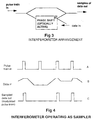
- an interferometer arrangement including a phase shift means 20.
- An optical pulse train is input at one side of the interferometer.
- Optical data is input at either side of the interferometer, but to only one arm of the interferometer, so as to alter the condition of interference of the interferometer.
- the phase shift means 20 can be arranged so that there is constructive interference when the data is high.
- the arrangement can be made in inverting form, so that there is constructive interference when the data is low.
- the peak output, where there is constructive interference can be arranged to coincide with the data beam at some point in-between high and low levels.
- Figure 4 shows input and output waveforms for the interferometer of figure 3 operating as a sampler.
- a pulse train A is input to both arms of the interferometer.
- Data in optical form is input to one of the arms.
- the phase shift means 20 typically implemented using a semiconductor optical amplifier, causes a phase shift in one arm, which results in the output waveform C of figure 4.
- the pulse train is output in a similar form to the pulse train input, owing to constructive interference. Where the data level is low, owing to destructive interference, there is little or no output. Accordingly, effectively the output can be seen as the pulse train input modulated by the data, or it can be seen as samples of the data, sampled by the input pulses.
- non-loop interferometer In principle, various types of non-loop interferometer could be used.
- the Mach-Zehnder type may be easiest to integrate and give best results in terms of stability and ease of tuning.
- a Michelson type interferometer could also be used.
- Figure 3 shows the data being fed in the interferometer in the opposite direction to the pulse train. This means the arrangement is simpler because the data does not need to be filtered out of the output. In principle the data could be fed into the interferometer in the same direction as the pulse train, in which case filtering would be needed to remove the data signal from the output.
- the first and second relate to optical clock recovery.
- the third type relates to sampling a signal to regenerate it optically without conversion to electrical form.
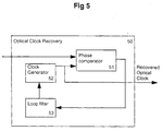
- Figure 5 shows an optical clock recovery arrangement 50 including a phase comparator 51, a clock generator 52, and a phase loop filter 53. Conventionally, such an arrangement has been produced for electrical signals, but it has been possible to achieve an optical phase comparator only suitable for operation with optical signals on which the data is coded in RZ form.
- the phase comparator receives the optical data input signal and an optical clock generated by the generator 52.
- the loop filter 53 can operate effectively with a bandwidth much lower than that of the optical data signal. Accordingly, it is feasible and less expensive to implement the clock phase control and the clock generator in electrical form, and convert the electrical clock to optical form before input to the phase comparator.
- the optical phase comparator 51 is shown in schematic form in figure 6.
- An interferometer 61 is provided for modulating the clock with the optical data.
- the interferometer is biased to give a peak output when the data is somewhere between high and low states, and a reduced output at the high and low states. This enables the interferometer to be responsive to data transitions, and thus determine timing of pulses optically.
- the interferometer may be arranged as shown in figure 3.
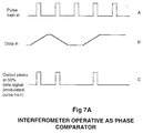
- Figure 7A shows the typical waveforms when the interferometer is used as a phase comparator, arranged to give peak output when the data is halfway between high and low states.
- the output peaks shown in waveform C of figure 7 would become changed in amplitude.
- the output pulse train would be passed through integration and low pass filtering functions 62. These would enable the phase comparator output to be independent of data patterns since there will be an averaging effect.
- this can be implemented by a PIN diode which would output a low speed electrical signal, typically with a bandwidth of up to hundreds of KiloHertz or a few MegaHertz, which can be fed back as shown in figure 5 to the loop filter 53, which is an analog low pass filter.
- the output of the filter is connected to the frequency control of the oscillator.
- a change in the amplitude of the pulses from the interferometer could be detected as a change in the level of the integrated filtered output of the PIN diode, which could cause the frequency of the oscillator to adjust to compensate.
- phase locked loop methods are well known and will not be described here in more detail.
- the output of the low frequency optical to electrical converter is the convolution of the power in these pulses with its impulse response. For conceptual simplicity, this can be thought of as approximately the integral of the power in the pulses over a response time of many thousands of pulses. Thus data with uneven amounts of ones and zeroes can be handled , provided fluctuations in the proportions of ones and zeroes don't have appreciable components at frequencies below the threshold of the converter.
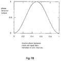
- the pulses output by the interferometer will be the strongest when the clock input pulses coincide with the data being at the 50% cross-over point, and will fall off with the cosine function as the data approaches a 1 or 0 symbol.
- the input data will not have a square waveform but may approach a raised cosine shape.
- the overall response of the phase detector after integration by a low pass filter is shown in figure 7B.
- the phase locked loop is advantageously locked to the 0.5 level of the phase detector output, and optical delay used to obtain the desired clock to data phase. Locking to the 0.5 level of the detector output gives the maximum control range (between 0 and 0.5 unit intervals of relative phase), and uses the steepest slope on the response curve, for strong feedback of phase error.
- the clock pulses are preferably generated at the full bit-rate, though sub-harmonics could be used.
- phase comparator can be implemented which enables the clock to be recovered independently of the type of coding used for the data.
- it can operate on NRZ data, as used in most high bit rate optical transmission systems.
- Figure 8 illustrates the second optical clock recovery arrangement 70, comprising a non-linear function operating on the optical data, 71, followed by an optical narrow band filter 72 to extract the clock frequency.
- the use of a non-linear function enables the clock to be recovered from data such as NRZ data for which there is little energy at the clock frequency.
- the non-linear function creates a response at the clock frequency.
- Figure 9 shows how the non-linear function 71 can be implemented by an interferometer 80, arranged as in figure 3. Instead of an input optical pulse train, because there is no separately generated clock, continuous wave light is input. This is modulated by the optical data, and the interferometer is biased to give a peak output at data transitions, as described above in relation to figure 7. If an optical pulse is output for each data transition, by the non-linear function 71, the optical narrow band filter 72 shown in figure 8 can be used to remove all but the clock frequency.
- the optical narrow band filter is implemented by a means of a mode-locked laser, although alternative implementations are conceivable.
- the arrangement of figure 10 can be used.
- the difference between outputs of two samplers 91, 92, operating as phase comparators, are subtracted to cancel common mode effects.
- a delay element 93 is provided to delay the clock input of one of the phase comparators. The delay can be arranged to be such that there is a minimal response from one of the comparators when the other is giving a peak output.
- the outputs of the samplers 91, 92 are integrated and filtered by optical to electrical converters 94 and 95.
- a subtractor 96 and low pass filter 97 can be used to derive an oscillator tuning signal from which common mode effects have been cancelled out.
- optical clock recovery circuits discussed above can be used in receivers or regenerators. They can be used in conjunction with electrical signal reshaping and retiming, or used with optical retiming and reshaping functions, to create an all optical regenerator, as shown in figure 11.
- Sampler 100 is fed by the output of the optical clock recovery function 101.
- a similar arrangement may occur at a receiver, where the optical sampler 100 is used for retiming and reshaping the optical data prior to conversion to electrical form, and subsequent processing such as demultiplexing.
- Figure 12 shows the optical regenerator of figure 11 in more detail.
- the sampler 100 comprises an interferometer, biased to give maximum output when the data input is in a given logical state.
- the optical recovery circuit 101 also comprises an interferometer, this time biased to produce a peak output on data transitions, to enable it to function as a phase comparator.
- a semiconductor optical amplifier 102 acts as the optically active element for changing the interference condition of the interferometer, according to the data signal fed into the same arm of the interferometer.
- Phase shift means 103 is provided for biasing the interferometer to achieve the desired function.
- a low pass filter 104 and optical clock 105 complete the phase locked loop, to lock the optical clock to the transitions in the data.
- a semiconductor optical amplifier (SOA) is again provided to alter the interference condition according to the data signal, and phase shift means 107 is provided to bias the interferometer to achieve the sampling function.
- SOA semiconductor optical amplifier
- an all optical regenerator can be achieved capable of handling NRZ data and capable of being integrated for cost effective regeneration, particularly suitable for higher bit rate transmission systems where electrical regeneration becomes more difficult and expensive.
- Figure 13 and 14 show applications of the optical sampler as illustrated in figure 12 or in figure 3, in multiplexer arrangements.
- Figure 13 shows a multiplexer arrangement in which multiplexing is carried out by optical or electrical multiplex means 110, and then an optical sampler 111 is provided to retime and reshape the combined signal, for onward transmission. Synchronisation is provided by clocks 112. Two clocks could be provided to the multiplexer 110 to switch the two incoming data streams appropriately to enable time division multiplexing. This could be on the basis of a bit interleave scheme, though other well known schemes are conceivable. Although only two data inputs are shown, obviously there could be more.
- FIG 14. An alternative multiplexer arrangement using the optical sampler described above, is shown in figure 14.
- An optical sampler 111 is provided for each of the optical data inputs to be multiplexed. Separate clocks are provided for each sampler so as to sample each optical data input at a different time interval. The mutually out of phase output samples can then be combined optically to produce a single multiplexed optical data output stream.
- Figures 15 and 16 show corresponding demultiplexing arrangements using the optical sampler described above.
- the sampler 111 is used to retime and reshape the incoming optical data stream. This enables the optical or electrical demultiplexer 120 to be of lower performance specification, since it is fed with a clean optical signal with little jitter.
- Figure 16 shows an alternative arrangement, in which multiple optical samplers 111 are fed with the same input data stream. Separate clocks are provided for each sampler so that samples are taken at different times by different samplers. This enables the time division multiplexed data to be separated out.
- demultiplexer arrangements of figures 15 and 16 could be used to decode multilevel logic signals. Different samplers could be biased individually so as to give a maximum output for different amplitude levels.
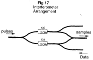
- figure 17 shows an arrangement in which the optically active element, the optical amplifier is provided in both arms of the interferometer.
- the interference condition of the interferometer and therefore the response at the output, is dependent on the amplitude of the modulation of the optical waveform, and on the phase of the optical waveform in each arm, ignoring polarisation effects.
- the optical amplifiers 130 and 131 in figure 17 can alter the interference condition.
- the interference condition will be changed because the optical amplifier has an amplitude to optical phase conversion effect.
- the pulses input to both arms are sufficiently short and have sufficiently low energy that the SOA does not react much to the pulses.
- the SOA should have a sufficiently rapid response time to react to the data waveform.
- the pulses input to both arms of the interferometer can therefore be very narrow, as there is no limit imposed by the speed of the response of the SOAs.
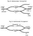
- Figure 18 shows an alternative arrangement in which a continuous wave bias is fed in in addition to the input pulses. This enables the operating point of the amplifiers to be set. A filter 140 would be required to remove the continuous wave from the output. In this figure and in figure 17, an output path at the top right is shown, which is unused, and provided only for balancing the arrangement.
- Figure 19 shows another interferometer arrangement in which one of the optical amplifiers is replaced with an electrically controlled phase shifter.
- phase shifter An example of such a phase shifter is described in Photonics Technology Letters, June 1990, pages 404 to 406, and Photonics Technology Letters, August 1996, pages 1018 to 1020 (Rolland et al).
- the gain/loss of the arm containing the phase shifter can be adjusted to match that in the arm containing the SOA.
- the phase shifter can be used to set the desired condition of interference, to enable peak output for the data input logic state being high, or low, or somewhere in between, as desired.
- One advantage of using such an optically passive device is that less ASE (amplified spontaneous emission) noise is generated. Furthermore, by using a phase shift device with little or no gain variation, the interference condition can be controlled more easily, since there is independent control of gain and phase differences between the two arms.
- the electrically controlled phase shifter need only operate at low frequencies, eg below 1 Megahertz, when only used for tuning. If a high frequency phase shifter were to be provided, then combined optical and electrical data inputs could be handled.
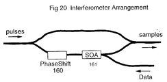
- Figure 20 shows another interferometer arrangement. If the phase shifter 160 is placed in the same arm as the SOA 161, the other arm becomes a simple transmission line. This has the advantage of better balance in the losses between the two arms. The phase shift will tend to attenuate the signal. The SOA can compensate for this by amplifying the signal. Electrically tuned attenuators could also be added to either arm, to balance the power levels. Other elements which have an optical phase shift in response to an optical power level could be used in place of the SOA. Other interferometer configuration such as a Michelson arrangement could be used. The entire device could be integrated for a low cost high volume production, using methods such as those discussed by Rolland et al.
- Figure 21 shows an arrangement which would be suitable for replacing the single interferometer of the sampler in figure 12.
- the first stage comprises an interferometer having SOAs 170 and 171. Continuous wave light is fed into both arms, and data is fed into one arm.
- the gain in the first stage can be arranged to be sufficient to drive the first stage output to its limit for one level of input data (high or low depending on whether the stage is to be inverting or not). This effectively makes gradual data transitions steeper, and flattens one of the logic states.
- the second stage can be arranged to drive its output to its limit for the other logic level.
- the data can be reshaped optically. If no retiming is required, but only reshaping, the second stage could be fed with continuous wave light. Alternatively, the retiming could be implemented by feeding the first stage with a pulse train.
- Figure 22 shows the output power for the first stage versus input power, where the first stage is an inverting stage.
- the power output is high, driving the output to its limit, and thus flattening the logic level 1 of the output.
- the output of the first stage should follow a response curve which is less steep than a 1/x curve at low input powers, and is flatter than the 1/x curve at higher input powers, but steeper at intermediate powers.
- Such a shape when used in two stages results in the overall response shown in figure 23.
- the transition range should be as short as possible.
- the transition range should be located so as to be centred around the threshold between high and low logic states for the input signal. If inverting devices are used, the transition can be centred more easily since the inversion causes the second stage response to balance the steepest portion of the first stage response, rather than accentuate it.
- a device with more than two stages could be constructed. Furthermore, the stages could be in parallel rather than in series. If in parallel, some sort of time division multiplexing for the two logic states would be required. Furthermore, the stages could be non-inverting, though for interferometers at least, the inverting response is preferable. Optical devices other than interferometers could be used if they have a non-linear response similar to that shown in figure 22.
- a short transition range will determine how steep the transitions of the change in interference condition of the second interferometer are. In turn, this can effect the sampling process which takes place in the second stage. If the second stage is fed by continuous wave light, the steepness of transition in interference condition will determine the shape of the output data transitions.
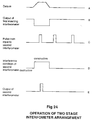
- Figure 24 shows at waveform A the data input.
- the output of the first inverting interferometer is shown in waveform B, which has steeper transitions than waveform A.
- the pulse train of waveform C is the other input to the second interferometer.
- Waveform D shows how the interference condition of the second interferometer is dependent on the output of the first interferometer.
- the limiting action of the first interferometer would remove noise from the signal for the period when the data input is in a high state. However, noise at the low state of the data input, would remain on the output of the first inverting interferometer. However, the interference condition of the second interferometer, shown in waveform D, would exhibit little noise on either the high level state or the low level state. Furthermore, the transitions in waveform D would be even steeper than those in waveform B, owing to the response of the type shown in figure 22. This leaves a relatively wide "eye", for the sampling pulse of the pulse train in waveform C. Accordingly, the output waveform E in figure 24 will be relatively free of noise, and relatively immune to jitter in the data input.
- the regeneration performance may not be as good in terms of jitter immunity and noise reduction, as can be achieved with electrical regeneration.
- the gain is limited to a factor of 3
- a signal at 10% above the threshold between high and low might be increased to 30% above the threshold.
- the threshold is set at 50% of the maximum signal, then the output would be up to 80% of the maximum, and therefore the limiting action would be only partial. Nevertheless, it would clearly be beneficial, even without complete limiting up to 100% of the signal range.
- the overall response shape can be altered by altering the relative gains of the two stages. This adds an extra degree of freedom.
- the amplification characteristics of the optical amplifiers in the interferometers can be varied.
- the relative powers of the three inputs, the data input, the continuous wave input, and the pulse train input, can be varied.
- the coupling between the two stages can be varied. In this way, the two stage device offers more flexibility for tailoring the response to the needs of the particular application.
- partial optical regeneration would be useful if applied between WDM subnetworks, for purposes of at least partial isolation, so that each subnetwork could be operated and specified independently of the degradations occurring in neighbouring networks.
Abstract
Description
a first and a second stage, both having non-linear responses, wherein the first stage has a limiting action on the input data signal when the signal as input to the arrangement is at a first logic state, the second stage has a limiting action when the signal as input to the arrangement is at a second logic state.
Claims (32)
- A method of modulating a pulse train comprising the steps of:inputting the pulse train to a non-loop interferometer;inputting an optical data stream to the interferometer, to obtain an output of the pulse train modulated according to the data stream.
- The method of claim 1 wherein the interferometer comprises a two arm interferometer, and the pulse train is input to both arms.
- The method of claim 2 wherein each of the two arms comprises a means for altering a condition of interference of the interferometer.
- The method of claim 2 or 3 wherein at least one of the arms comprises an electrically controllable means for altering a condition of interference of the interferometer.
- A method of retiming an optical data signal comprising the steps of:generating a pulse train;modulating the pulse train using the method of any preceding claim.
- The method of claim 5 wherein the step of generating a pulse train comprises the step of recovering a clock from the optical data signal.
- The method of claim 6 wherein the clock is recovered optically.
- A method of time division multiplexing optical data signals, comprising the steps of:sampling the optical data signals at mutually different phases, each sampling process using the method of any of claims 1 to 4; andcombining the sampled data signals.
- A method of multiplexing signals comprising the steps of:combining the signals to create an optical multiplexed data signal; andretiming the multiplexed data signal by using it to modulate a pulse train according to the method of any of claims1 to 4.
- A method of demultiplexing at least a portion of a time division multiplexed optical signal comprising the steps of:generating a pulse train synchronised with the portion to be demultiplexed; andsampling the portion using the method of any of claims 1 to 4 to separate it from the multiplexed signal.
- A method of demultiplexing an optical multiplexed data signal comprising the steps of:retiming the signal by using it to modulate a pulse train according to the method of any of claims 1 to 4; anddemultiplexing the retimed signal.
- A method of operating an optical transmission system comprising a transmitter and a receiver, the method comprising the steps of:
transmitting an optical data signal to the receiver, and retiming the optical data signal at the receiver by using it to modulate a pulse train according to the method of any of claims 1 to 4. - A method of operating an interferometer, the interferometer comprising an optically induced means for altering a condition of interference, and an optically passive means for altering the condition of the interference, the method comprising the steps of:inputting an optical signal to alter the interference condition,controlling the optically passive means to vary the response of the interference condition to the optical signal.
- The method of claim 13 wherein the interferometer comprises a two arm type interferometer.
- The method of claim 14 wherein the optically induced means and the optically passive means act on the same arm of the interferometer.
- An optical sampler for sampling an optical data stream, comprising:means for providing an optical pulse train;a non loop interferometer arranged to modulate the pulse train according to the data stream.
- The sampler of claim 16 wherein the interferometer comprises a two arm type interferometer.
- The sampler of claim 16 or 17 wherein the interferometer comprises an optically induced means for altering a condition of interference of the interferometer.
- The sampler of claim 18 wherein the optically induced means comprises a semiconductor optical amplifier.
- The sampler of any of claims 16 to 19 further comprising a means for electrically controlling the response of a condition of interference of the interferometer to the data signal.
- A regenerator for regenerating an optical data signal, comprising:the sampler of any of claims 16 to 20; anda clock recovery means for recovering a clock from the optical data signal.
- An optical terminal for an optical transmission system, comprising:the sampler of any of claims 16 to 20; andmeans for converting the data stream between electrical and optical form.
- An interferometer comprising:an input for an optical signal;an input for a control signal;an optically induced means for altering a condition of interference of the interferometer in response to the optical signal; andan optically passive means for altering the response interference condition to the optical signal, according to the control signal.
- The interferometer of claim 23 wherein the optically induced means comprises an optical amplifier.
- The interferometer of claim 23 or 24, wherein the optically passive means comprises an electrically controlled element.
- The interferometer of claim 25 wherein the electrically controlled element comprises a phase shift means.
- The interferometer of any of claims 23 to 26 further comprising control means for generating the control signal at low frequencies for tuning the response to maintain a constant output.
- A regenerator for regenerating an optical data signal, comprising:means for recovering a clock from the optical data signal; anda sampling means synchronised by the recovered clock, wherein the sampling means comprises the interferometer of any of claims 23 to 27.
- An optical pulse reshaping arrangement for reshaping an input data signal, the arrangement comprising:
a first and a second stage, both having non-linear responses, wherein the first stage has a limiting action on the input data signal when the signal as input to the arrangement is at a first logic state, the second stage has a limiting action when the signal as input to the arrangement is at a second logic state. - The arrangement of claim 29 wherein the two stages are arranged in series.
- The arrangement of claim 29 or 30 wherein both stages have an inverting action.
- The arrangement of any of claims 29 to 31 wherein the non-linear responses of the two stages have different shapes.
Applications Claiming Priority (4)
| Application Number | Priority Date | Filing Date | Title |
|---|---|---|---|
| GB9626373 | 1996-12-19 | ||
| GB9626373A GB2320634A (en) | 1996-12-19 | 1996-12-19 | Optical sampling by using an interferometer to modulate a pulse train |
| US08/865,492 US6229633B1 (en) | 1996-12-19 | 1997-05-29 | Optical sampling by modulating a pulse train |
| US865492 | 1997-05-29 |
Publications (3)
| Publication Number | Publication Date |
|---|---|
| EP0849622A2 true EP0849622A2 (en) | 1998-06-24 |
| EP0849622A3 EP0849622A3 (en) | 1999-10-13 |
| EP0849622B1 EP0849622B1 (en) | 2003-09-10 |
Family
ID=26310679
Family Applications (1)
| Application Number | Title | Priority Date | Filing Date |
|---|---|---|---|
| EP97309354A Expired - Lifetime EP0849622B1 (en) | 1996-12-19 | 1997-11-20 | All-optical sampling by modulating a pulse train |
Country Status (4)
| Country | Link |
|---|---|
| EP (1) | EP0849622B1 (en) |
| JP (1) | JPH10293332A (en) |
| CA (1) | CA2222666C (en) |
| DE (1) | DE69724750T2 (en) |
Cited By (4)
| Publication number | Priority date | Publication date | Assignee | Title |
|---|---|---|---|---|
| FR2803698A1 (en) * | 2000-01-12 | 2001-07-13 | Cit Alcatel | 3R REGENERATION OF AN OPTICAL SIGNAL |
| EP1383255A2 (en) * | 2002-07-20 | 2004-01-21 | Samsung Electronics Co., Ltd. | Apparatus for regenerating all-optical signal and method thereof |
| EP1599957A2 (en) * | 2003-03-05 | 2005-11-30 | Ecological Wireless Solutions Ltd. | Optical time division multiplexing |
| FR3020526A1 (en) * | 2014-04-28 | 2015-10-30 | Thales Sa | METHOD FOR GENERATING M DEMODULATION SIGNALS |
Families Citing this family (1)
| Publication number | Priority date | Publication date | Assignee | Title |
|---|---|---|---|---|
| JP4949620B2 (en) * | 2004-03-31 | 2012-06-13 | 富士通株式会社 | Optical waveform shaper |
Citations (2)
| Publication number | Priority date | Publication date | Assignee | Title |
|---|---|---|---|---|
| US3724926A (en) * | 1971-08-09 | 1973-04-03 | Bell Telephone Labor Inc | Optical pulse modulator |
| WO1996022562A1 (en) * | 1995-01-19 | 1996-07-25 | British Telecommunications Public Limited Company | Optical switch |
-
1997
- 1997-11-20 DE DE69724750T patent/DE69724750T2/en not_active Expired - Lifetime
- 1997-11-20 EP EP97309354A patent/EP0849622B1/en not_active Expired - Lifetime
- 1997-11-26 CA CA002222666A patent/CA2222666C/en not_active Expired - Fee Related
- 1997-12-19 JP JP9364998A patent/JPH10293332A/en active Pending
Patent Citations (2)
| Publication number | Priority date | Publication date | Assignee | Title |
|---|---|---|---|---|
| US3724926A (en) * | 1971-08-09 | 1973-04-03 | Bell Telephone Labor Inc | Optical pulse modulator |
| WO1996022562A1 (en) * | 1995-01-19 | 1996-07-25 | British Telecommunications Public Limited Company | Optical switch |
Non-Patent Citations (8)
| Title |
|---|
| AGRAWAL N ET AL: "Optical signal processing using monolithically integrated semiconductor laser amplifier structures" OSA TRENDS IN OPTICS AND PHOTONICS (OSA TOPS) VOL.5 - OPTICAL AMPLIFIERS AND THEIR APPLICATIONS - FROM THE TOPICAL MEETING, MONTEREY, CA, USA, 11-13 JULY 1996, pages 205-220, XP002084133 ISBN 1-55752-435-X, 1996, Washington, DC, USA, Opt. Soc. America, USA * |
| JINNO M: "All optical signal regularizing/regeneration using a nonlinear fiber Sagnac interferometer switch with signal-clock walk-off" JOURNAL OF LIGHTWAVE TECHNOLOGY, SEPT. 1994, USA, ISSN 0733-8724, vol. 12, no. 9, pages 1648-1659, XP000484344 * |
| JOERGENSEN C ET AL: "Wavelength conversion by optimized monolithic integrated Mach-Zehnder interferometer" IEEE PHOTONICS TECHNOLOGY LETTERS, APRIL 1996, IEEE, USA, ISSN 1041-1135, vol. 8, no. 4, pages 521-523, XP000587013 * |
| MIKKELSEN B ET AL: "Polarisation insensitive wavelength conversion of 10 Gbit/s signals with SOAs in a Michelson interferometer" ELECTRONICS LETTERS, 3 FEB. 1994, UK, ISSN 0013-5194, vol. 30, no. 3, pages 260-261, XP000431304 * |
| MIKKELSEN B ET AL: "Wavelength conversion devices" OPTICAL FIBER COMMUNICATION (OFC) 1996, SAN JOSE, FEB. 25 - MAR. 1, 1996, PAPER WG1, vol. 2, no. CONG. 19, 25 February 1996, pages 121-122, XP002101384 OPTICAL SOCIETY OF AMERICA * |
| RATOVELOMANANA F ET AL: "Regeneration improvement in all-optical wavelength converter, based on a Mach-Zehnder interferometer, by means of phase-shifter section" ELECTRONICS LETTERS, 11 SEPT. 1997, IEE, UK, ISSN 0013-5194, vol. 33, no. 19, pages 1629-1630, XP000739626 * |
| SILBERBERG Y: "NON-LINEAR ALL-OPTICAL REGENERATORS" CONFERENCE ON LASERS AND ELECTRO-OPTICS, 9 - 13 June 1986, XP002104403 * |
| SIMON J C ET AL: "TWO-STAGE WAVELENGTH CONVERTER WITH IMPROVED EXTINCTION RATIO" OPTICAL FIBER COMMUNICATION. SUMMARIES OF PAPERS PRESENTED AT THE CONFERENCE OFC '95, SAN DIEGO, FEB. 26 - MAR. 3, 1995, 1 January 1995, pages 381-384, XP000653653 INSTITUTE OF ELECTRICAL AND ELECTRONICS ENGINEERS * |
Cited By (13)
| Publication number | Priority date | Publication date | Assignee | Title |
|---|---|---|---|---|
| US6775481B2 (en) | 2000-01-12 | 2004-08-10 | Alcatel | 3R optical signal regeneration |
| EP1117199A1 (en) * | 2000-01-12 | 2001-07-18 | Alcatel | 3R-regeneration of an optical signal |
| FR2803698A1 (en) * | 2000-01-12 | 2001-07-13 | Cit Alcatel | 3R REGENERATION OF AN OPTICAL SIGNAL |
| US7085498B2 (en) | 2002-07-20 | 2006-08-01 | Samsung Electronics Co., Ltd. | Apparatus for regenerating all-optical signal and method thereof |
| EP1383255A3 (en) * | 2002-07-20 | 2005-06-15 | Samsung Electronics Co., Ltd. | Apparatus for regenerating all-optical signal and method thereof |
| EP1383255A2 (en) * | 2002-07-20 | 2004-01-21 | Samsung Electronics Co., Ltd. | Apparatus for regenerating all-optical signal and method thereof |
| CN1305235C (en) * | 2002-07-20 | 2007-03-14 | 三星电子株式会社 | Equipment for regenerating all-optical signal and its method |
| EP1599957A2 (en) * | 2003-03-05 | 2005-11-30 | Ecological Wireless Solutions Ltd. | Optical time division multiplexing |
| EP1599957A4 (en) * | 2003-03-05 | 2007-05-02 | Optiway Ltd | Optical time division multiplexing |
| US7627247B2 (en) | 2003-03-05 | 2009-12-01 | Optiway Ltd. | Optical time division multiplexing |
| FR3020526A1 (en) * | 2014-04-28 | 2015-10-30 | Thales Sa | METHOD FOR GENERATING M DEMODULATION SIGNALS |
| EP2940522A1 (en) * | 2014-04-28 | 2015-11-04 | Thales | Method for generating m demodulation signals |
| US9441949B2 (en) | 2014-04-28 | 2016-09-13 | Thales | Method for generating M demodulation signals using at least one primary interferometer |
Also Published As
| Publication number | Publication date |
|---|---|
| EP0849622B1 (en) | 2003-09-10 |
| CA2222666C (en) | 2002-01-15 |
| CA2222666A1 (en) | 1998-06-19 |
| DE69724750D1 (en) | 2003-10-16 |
| EP0849622A3 (en) | 1999-10-13 |
| DE69724750T2 (en) | 2004-03-25 |
| JPH10293332A (en) | 1998-11-04 |
Similar Documents
| Publication | Publication Date | Title |
|---|---|---|
| US6229633B1 (en) | Optical sampling by modulating a pulse train | |
| US6282007B1 (en) | Optical timing detection | |
| US20030011847A1 (en) | Method and apparatus for adaptive distortion compensation in optical fiber communication networks | |
| US6735398B1 (en) | Generating methods for single and multi-channel wideband optical analog pulse positioned waveforms | |
| US5798852A (en) | All-optical device for regenerating an optical signal modulated in an RZ format | |
| US6323991B2 (en) | Opto-electronic frequency divider circuit and method of operating same | |
| CA2222669C (en) | Optical timing detection | |
| US7623792B2 (en) | Clock extracting method and apparatus thereof | |
| US6396607B1 (en) | Multi-wavelength all-optical regenerators (MARS) | |
| JP2711773B2 (en) | Optical waveform shaping device | |
| US6448913B1 (en) | TOAD- based optical data format converter | |
| US7574139B2 (en) | Carrier-suppressed optical time domain multiplexing | |
| US7035550B2 (en) | All-optical, 3R regeneration using the Sagnac and Mach-Zehnder versions of the terahertz optical asymmetric demultiplexer (TOAD) | |
| US20090208216A1 (en) | Dispersion compensation | |
| CA2222666C (en) | Optical sampling by modulating a pulse train | |
| EP0555063B1 (en) | Optical waveform shaping device | |
| JP4066588B2 (en) | Optical receiver | |
| JP2004530312A (en) | All-optical circuitry independent of bit rate and format for reshaping, reproducing, and timing of optical pulse streams | |
| EP1298831A1 (en) | A CA-RZ optical clock signal generator, and a resynchronized optical multiplexer containing such a generator | |
| JP3752540B2 (en) | Optical pulse separation method and optical pulse separation device | |
| EP1344340A2 (en) | Demultiplexer for high data rate signals | |
| WO2003013032A1 (en) | Optical signal regeneration |
Legal Events
| Date | Code | Title | Description |
|---|---|---|---|
| PUAI | Public reference made under article 153(3) epc to a published international application that has entered the european phase |
Free format text: ORIGINAL CODE: 0009012 |
|
| AK | Designated contracting states |
Kind code of ref document: A2 Designated state(s): DE FR GB NL SE |
|
| AX | Request for extension of the european patent |
Free format text: AL;LT;LV;MK;RO;SI |
|
| RAP3 | Party data changed (applicant data changed or rights of an application transferred) |
Owner name: NORTEL NETWORKS CORPORATION |
|
| PUAL | Search report despatched |
Free format text: ORIGINAL CODE: 0009013 |
|
| AK | Designated contracting states |
Kind code of ref document: A3 Designated state(s): AT BE CH DE DK ES FI FR GB GR IE IT LI LU MC NL PT SE |
|
| AX | Request for extension of the european patent |
Free format text: AL;LT;LV;MK;RO;SI |
|
| 17P | Request for examination filed |
Effective date: 20000413 |
|
| AKX | Designation fees paid |
Free format text: DE FR GB NL SE |
|
| RAP1 | Party data changed (applicant data changed or rights of an application transferred) |
Owner name: NORTEL NETWORKS LIMITED |
|
| 17Q | First examination report despatched |
Effective date: 20010706 |
|
| GRAH | Despatch of communication of intention to grant a patent |
Free format text: ORIGINAL CODE: EPIDOS IGRA |
|
| GRAS | Grant fee paid |
Free format text: ORIGINAL CODE: EPIDOSNIGR3 |
|
| GRAA | (expected) grant |
Free format text: ORIGINAL CODE: 0009210 |
|
| AK | Designated contracting states |
Kind code of ref document: B1 Designated state(s): DE FR GB NL SE |
|
| PG25 | Lapsed in a contracting state [announced via postgrant information from national office to epo] |
Ref country code: NL Free format text: LAPSE BECAUSE OF FAILURE TO SUBMIT A TRANSLATION OF THE DESCRIPTION OR TO PAY THE FEE WITHIN THE PRESCRIBED TIME-LIMIT Effective date: 20030910 |
|
| REG | Reference to a national code |
Ref country code: GB Ref legal event code: FG4D |
|
| RAP2 | Party data changed (patent owner data changed or rights of a patent transferred) |
Owner name: NORTEL NETWORKS LIMITED |
|
| REF | Corresponds to: |
Ref document number: 69724750 Country of ref document: DE Date of ref document: 20031016 Kind code of ref document: P |
|
| NLT2 | Nl: modifications (of names), taken from the european patent patent bulletin |
Owner name: NORTEL NETWORKS LIMITED |
|
| PG25 | Lapsed in a contracting state [announced via postgrant information from national office to epo] |
Ref country code: SE Free format text: LAPSE BECAUSE OF FAILURE TO SUBMIT A TRANSLATION OF THE DESCRIPTION OR TO PAY THE FEE WITHIN THE PRESCRIBED TIME-LIMIT Effective date: 20031210 |
|
| NLV1 | Nl: lapsed or annulled due to failure to fulfill the requirements of art. 29p and 29m of the patents act | ||
| ET | Fr: translation filed | ||
| PLBE | No opposition filed within time limit |
Free format text: ORIGINAL CODE: 0009261 |
|
| STAA | Information on the status of an ep patent application or granted ep patent |
Free format text: STATUS: NO OPPOSITION FILED WITHIN TIME LIMIT |
|
| 26N | No opposition filed |
Effective date: 20040614 |
|
| PGFP | Annual fee paid to national office [announced via postgrant information from national office to epo] |
Ref country code: DE Payment date: 20141201 Year of fee payment: 18 Ref country code: FR Payment date: 20141027 Year of fee payment: 18 Ref country code: GB Payment date: 20141027 Year of fee payment: 18 |
|
| REG | Reference to a national code |
Ref country code: DE Ref legal event code: R119 Ref document number: 69724750 Country of ref document: DE |
|
| GBPC | Gb: european patent ceased through non-payment of renewal fee |
Effective date: 20151120 |
|
| REG | Reference to a national code |
Ref country code: FR Ref legal event code: ST Effective date: 20160729 |
|
| PG25 | Lapsed in a contracting state [announced via postgrant information from national office to epo] |
Ref country code: GB Free format text: LAPSE BECAUSE OF NON-PAYMENT OF DUE FEES Effective date: 20151120 Ref country code: DE Free format text: LAPSE BECAUSE OF NON-PAYMENT OF DUE FEES Effective date: 20160601 |
|
| PG25 | Lapsed in a contracting state [announced via postgrant information from national office to epo] |
Ref country code: FR Free format text: LAPSE BECAUSE OF NON-PAYMENT OF DUE FEES Effective date: 20151130 |