EP1271782A2 - FPGA with at least two different and independently configurable memory structures - Google Patents
FPGA with at least two different and independently configurable memory structures Download PDFInfo
- Publication number
- EP1271782A2 EP1271782A2 EP02012610A EP02012610A EP1271782A2 EP 1271782 A2 EP1271782 A2 EP 1271782A2 EP 02012610 A EP02012610 A EP 02012610A EP 02012610 A EP02012610 A EP 02012610A EP 1271782 A2 EP1271782 A2 EP 1271782A2
- Authority
- EP
- European Patent Office
- Prior art keywords
- memory
- logic device
- programmable logic
- field programmable
- structures
- Prior art date
- Legal status (The legal status is an assumption and is not a legal conclusion. Google has not performed a legal analysis and makes no representation as to the accuracy of the status listed.)
- Granted
Links
Images


Classifications
-
- H—ELECTRICITY
- H03—ELECTRONIC CIRCUITRY
- H03K—PULSE TECHNIQUE
- H03K19/00—Logic circuits, i.e. having at least two inputs acting on one output; Inverting circuits
- H03K19/02—Logic circuits, i.e. having at least two inputs acting on one output; Inverting circuits using specified components
- H03K19/173—Logic circuits, i.e. having at least two inputs acting on one output; Inverting circuits using specified components using elementary logic circuits as components
- H03K19/177—Logic circuits, i.e. having at least two inputs acting on one output; Inverting circuits using specified components using elementary logic circuits as components arranged in matrix form
- H03K19/17748—Structural details of configuration resources
- H03K19/1776—Structural details of configuration resources for memories
-
- H—ELECTRICITY
- H03—ELECTRONIC CIRCUITRY
- H03K—PULSE TECHNIQUE
- H03K19/00—Logic circuits, i.e. having at least two inputs acting on one output; Inverting circuits
- H03K19/02—Logic circuits, i.e. having at least two inputs acting on one output; Inverting circuits using specified components
- H03K19/173—Logic circuits, i.e. having at least two inputs acting on one output; Inverting circuits using specified components using elementary logic circuits as components
- H03K19/177—Logic circuits, i.e. having at least two inputs acting on one output; Inverting circuits using specified components using elementary logic circuits as components arranged in matrix form
- H03K19/17736—Structural details of routing resources
Definitions
- the present invention relates to a field programmable logic device with efficient memory utilization.
- Configurable memories are embedded in field programmable logic devices to provide on-chip fast RAM.
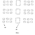
- memory resources There are two types of memory resources commercially available as shown in FIG 1.
- the first type are the LUTs inside Logic blocks 102 of FIG1, that can be combined in various fashions to provide memories of varying widths and depths as in Xilinx XC4000 and Virtex devices.
- a drawback with these distributed memory resources is that the large memory formed by combining these resources is slow.
- one has to provide read/write control circuitry with all LUTs. In case these LUTs are not used to implement memory then the read/write control circuitry associated with LUTs is wasted.
- the second type of on-chip memory resources is the large chunks/blocks of RAM bits 101 of FIG1, as provided by Xilinx and Altera. These can be configured to provide memories with varying widths and depths.
- a drawback associated with these resources is that if a block (of say 4k) is used to implement a small memory (say 512x2)), then there is wastage of unused RAM bits (3K). Moreover if a logical memory supports an odd width (say 256x9) then there is even more wastage of resources.
- the following scenario provides the motivation for providing heterogeneous memory structures in an FPGA or PLD.
- the object of this invention is to obviate the above drawbacks.
- this invention provides a field programmable logic device comprising at least two independently configurable embedded memory structures wherein said memory structures differ in at least one of the following parameter
- the said memory structures provide mutually exclusive configuration options in at least one configuration parameter
- the said memory structures are combined to form larger configurations through interconnection of dedicated memory routing tracks and horizontal routing channels
- the said dedicated memory routing tracks comprising plurality of bus based vertical tracks originating from memory IOs.
- the horizontal routing channels comprising several routing tracks.
- the said dedicated memory routing track interact with the horizontal routing channels through programmable switches.
- a single set of dedicated memory routing track spans one or more memory block and a plurality of horizontal routing channels
- the upper and lower end of dedicated memory routing tracks are a set of bus based bi-directional programmable buffers to connect different blocks of memory to form deeper and /or wider memories.
- each memory structure supports only a subset of total configuration modes available, the size of the multiplexer at the input/ output of said memories will be reduced thereby enhancing the speed of access to the memories.
- the said memory structures are used independently or in combination to implement logic functions.
- the said memory structures are multi-port.
- the said memory structures are Read Only Memory (ROM), Random Access Memory (RAM), Content Addressable Memory (CAM), First In First Out (FIFO) structures.
- ROM Read Only Memory
- RAM Random Access Memory
- CAM Content Addressable Memory
- FIFO First In First Out
- FIG2 represents the preferred type of Programmable Logic device that includes three types of programmable resources viz. 201, 202, 203.
- Component 201 represents programmable memory block with wider configurable data widths and/or larger core size with respect to component 202.
- Component 202 represents programmable memory block with smaller configurable data widths and/or smaller core size with respect to component 201.
- Component 203 represents programmable logic blocks that can be any of a PLA or LUT based circuit to implement logic intensive circuits.
- 202 of FIG2 supports small memory requirements (memory size) with plurality of smaller configurable word sizes for example x1, x2, and x4.
- the smaller configurable memory arrays can be combined using dedicated (bus-based) as well as general routing resources to create wider or deeper memories.
- 201 of FIG2 supports large memory requirements (memory size) with plurality of larger configurable word sizes as x8, x16, and x32.
- the larger memory arrays can also be combined using separate dedicated (bus-based) as well as general routing resources to create wider or deeper memories.
- each memory structure Since each memory structure is supporting only a subset of the total configuration modes available, the size of the multiplexer at the input/output of the memories will be reduced. Reduced flexibility at each level enhances the speed of operation at both levels, though it does not affect the overall number of possible combinations of different word sizes available. As the configuration modes supported by both types of memory structures are mutually exclusive they do interact with each other and no separate routing resources between the two types of memory structures are needed.
- FIG4 shows one of the preferred ways to implement a 256x9 logical memory that may be required in some designs.
- one block of 201 memory and one block of 202 memories are combined to form a memory block of size 256x9.
- the block of 202 memory is configured in 256x1 mode.
- 256x1 mode means that this memory has 256 words of 1 bit each. To address 256 words, this memory requires 8 address lines 401, and its output data bus 403, is 1 bit wide.
- the block of 201 memory is configured in 256x8 mode.
- 256x8 mode means that this memory has 256 words of 8 bit each. To address 256 words, this memory requires 8 address lines 402, and its output data bus 404, is 8 bits wide.
- the 201 and 202 blocks are combined in the following manner.
- the address buses of 202 block and 201 block, i.e., 401 and 402 are shorted.
- the short connection is provided through routing segments and programmable connections (see FIG4 ).
- the output data buses of both the blocks together, i.e., 403 and 404 represent the data bus, 405 of 256x9 memory.
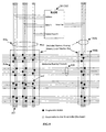
- FIG5 shows a preferred way of memory to memory and memory to logic interaction scheme.
- the memory block (any of 202 or 201) interacts with logic blocks 203, and other memory blocks through dedicated memory routing tracks and horizontal routing channels.
- the dedicated memory routing tracks (505a & 505b ) consist of plurality of bus-based vertical tracks (originating from memory I/Os) that interact with horizontal routing channels 508, through programmable switches, 400.
- the horizontal routing tracks in turn interact with logic blocks.
- the horizontal routing channels also consist of several routing tracks.
- the dedicated memory routing tracks interact with horizontal routing channels through programmable switches.
- a single set of dedicated memory routing tracks spans one (or more) memory block and a plurality of horizontal routing channels (as shown in the FIG5 ).
- a set of bus-based bi-directional programmable buffers 507 that help to connect different blocks of memories to form deeper and/or wider memories.
- connection box where dedicated memory routing tracks interact with horizontal routing channels is called Memory Logic Interface ( 506a & 506b ).
- Memory Logic Interface 506a & 506b .
- the interconnections between memory blocks and logic blocks are made possible with this Memory Logic Interface box. It is to be noted that the attached figure is only a representation of the case. In actual connections the number of address and data lines would be larger than shown in the figure.
- the different memory structures are distinguished on the basis of the configuration modes supported by them but have same size.
- both or any one of the memories can be used in asynchronous ROM mode to implement substantial logic when the design does not require all the on-chip memory resources provided thus saving LUTs in all the cases considered above.
- the above explanation can be easily extended to more than two types of memory resources.
Landscapes
- Physics & Mathematics (AREA)
- Mathematical Physics (AREA)
- Engineering & Computer Science (AREA)
- Computer Hardware Design (AREA)
- Computing Systems (AREA)
- General Engineering & Computer Science (AREA)
- Computer Networks & Wireless Communication (AREA)
- Logic Circuits (AREA)
- Design And Manufacture Of Integrated Circuits (AREA)
Abstract
- memory size
- available configuration depths
- available configuration widths
Description
- memory size
- available configuration depths
- available configuration widths
The above explanation can be easily extended to more than two types of memory resources.
Claims (12)
- A field programmable logic device comprising at least two independently configurable embedded memory structures wherein said memory structures differ in at least one of the following parameterfor efficient memory utilization.memory sizeavailable configuration depthsavailable configuration widths,
- A field programmable logic device as claimed in claim 1 wherein said memory structures provide mutually exclusive configuration options in at least one configuration parameter
- A field programmable logic device as claimed in claim 1 wherein said memory structures are combined to form larger configurations through interconnection of dedicated memory routing tracks and horizontal routing channels
- A field programmable logic device as claimed in claim 3 wherein said dedicated memory routing tracks comprising plurality of bus based vertical tracks originating from memory IOs.
- A field programmable logic device as claimed in claim 3 wherein horizontal routing channels comprising several routing tracks.
- A field programmable logic device as claimed in claim 3 wherein said dedicated memory routing track interact with the horizontal routing channels through programmable switches.
- A field programmable logic device as claimed in claim 3 wherein a single set of dedicated memory routing track spans one or more memory block and a plurality of horizontal routing channels
- A field programmable logic device as claimed in claim 3 wherein the upper and lower end of dedicated memory routing tracks are a set of bus based bi-directional programmable buffers to connect different blocks of memory to form deeper and / or wider memories.
- A field programmable logic device as claimed in claim 1 wherein since each memory structure supports only a subset of total configuration modes available, the size of the multiplexer at the input/ output of said memories will be reduced thereby enhancing the speed of access to the memories.
- A field programmable logic device as claimed in claim 1 wherein said memory structures are used independently or in combination to implement logic functions.
- A field programmable logic device as claimed in claim 1 wherein said memory structures are multi-port.
- A field programmable logic device as claimed in claim 1 wherein said memory structures are Read Only Memory (ROM), Random Access Memory (RAM), Content Addressable Memory (CAM), First In First Out (FIFO) structures.
Applications Claiming Priority (3)
| Application Number | Priority Date | Filing Date | Title |
|---|---|---|---|
| IN728DE2001 | 2001-06-29 | ||
| INDE07282001 | 2001-06-29 | ||
| INDE010728 | 2001-06-29 |
Publications (3)
| Publication Number | Publication Date |
|---|---|
| EP1271782A2 true EP1271782A2 (en) | 2003-01-02 |
| EP1271782A3 EP1271782A3 (en) | 2003-07-23 |
| EP1271782B1 EP1271782B1 (en) | 2005-05-18 |
Family
ID=11097079
Family Applications (1)
| Application Number | Title | Priority Date | Filing Date |
|---|---|---|---|
| EP02012610A Expired - Lifetime EP1271782B1 (en) | 2001-06-29 | 2002-06-06 | FPGA with at least two different and independently configurable memory structures |
Country Status (3)
| Country | Link |
|---|---|
| US (1) | US6788104B2 (en) |
| EP (1) | EP1271782B1 (en) |
| DE (1) | DE60204189T2 (en) |
Families Citing this family (82)
| Publication number | Priority date | Publication date | Assignee | Title |
|---|---|---|---|---|
| US6720796B1 (en) * | 2001-05-06 | 2004-04-13 | Altera Corporation | Multiple size memories in a programmable logic device |
| US6781408B1 (en) | 2002-04-24 | 2004-08-24 | Altera Corporation | Programmable logic device with routing channels |
| US7142011B1 (en) | 2002-04-24 | 2006-11-28 | Altera Corporation | Programmable logic device with routing channels |
| US7133972B2 (en) | 2002-06-07 | 2006-11-07 | Micron Technology, Inc. | Memory hub with internal cache and/or memory access prediction |
| US7117316B2 (en) | 2002-08-05 | 2006-10-03 | Micron Technology, Inc. | Memory hub and access method having internal row caching |
| US6820181B2 (en) | 2002-08-29 | 2004-11-16 | Micron Technology, Inc. | Method and system for controlling memory accesses to memory modules having a memory hub architecture |
| EP1639734A4 (en) * | 2003-06-06 | 2010-12-01 | Intellambda Systems Inc | TOPOLOGY DATABASES FOR OPTICAL NETWORKS AND OPERATIONS FOR OPTICAL NETWORKS |
| US7120727B2 (en) | 2003-06-19 | 2006-10-10 | Micron Technology, Inc. | Reconfigurable memory module and method |
| US7260685B2 (en) | 2003-06-20 | 2007-08-21 | Micron Technology, Inc. | Memory hub and access method having internal prefetch buffers |
| US7107415B2 (en) | 2003-06-20 | 2006-09-12 | Micron Technology, Inc. | Posted write buffers and methods of posting write requests in memory modules |
| US7170315B2 (en) | 2003-07-31 | 2007-01-30 | Actel Corporation | Programmable system on a chip |
| US7521960B2 (en) * | 2003-07-31 | 2009-04-21 | Actel Corporation | Integrated circuit including programmable logic and external-device chip-enable override control |
| US7120743B2 (en) | 2003-10-20 | 2006-10-10 | Micron Technology, Inc. | Arbitration system and method for memory responses in a hub-based memory system |
| US7330992B2 (en) | 2003-12-29 | 2008-02-12 | Micron Technology, Inc. | System and method for read synchronization of memory modules |
| US7188219B2 (en) | 2004-01-30 | 2007-03-06 | Micron Technology, Inc. | Buffer control system and method for a memory system having outstanding read and write request buffers |
| US7213082B2 (en) * | 2004-03-29 | 2007-05-01 | Micron Technology, Inc. | Memory hub and method for providing memory sequencing hints |
| US7138824B1 (en) | 2004-05-10 | 2006-11-21 | Actel Corporation | Integrated multi-function analog circuit including voltage, current, and temperature monitor and gate-driver circuit blocks |
| US7162567B2 (en) | 2004-05-14 | 2007-01-09 | Micron Technology, Inc. | Memory hub and method for memory sequencing |
| US7519788B2 (en) | 2004-06-04 | 2009-04-14 | Micron Technology, Inc. | System and method for an asynchronous data buffer having buffer write and read pointers |
| US7099189B1 (en) | 2004-10-05 | 2006-08-29 | Actel Corporation | SRAM cell controlled by non-volatile memory cell |
| US7116181B2 (en) | 2004-12-21 | 2006-10-03 | Actel Corporation | Voltage- and temperature-compensated RC oscillator circuit |
| US7119398B1 (en) | 2004-12-22 | 2006-10-10 | Actel Corporation | Power-up and power-down circuit for system-on-a-chip integrated circuit |
| US7446378B2 (en) * | 2004-12-29 | 2008-11-04 | Actel Corporation | ESD protection structure for I/O pad subject to both positive and negative voltages |
| US8620980B1 (en) | 2005-09-27 | 2013-12-31 | Altera Corporation | Programmable device with specialized multiplier blocks |
| US8301681B1 (en) | 2006-02-09 | 2012-10-30 | Altera Corporation | Specialized processing block for programmable logic device |
| US8266198B2 (en) | 2006-02-09 | 2012-09-11 | Altera Corporation | Specialized processing block for programmable logic device |
| US8041759B1 (en) | 2006-02-09 | 2011-10-18 | Altera Corporation | Specialized processing block for programmable logic device |
| US8266199B2 (en) | 2006-02-09 | 2012-09-11 | Altera Corporation | Specialized processing block for programmable logic device |
| US7836117B1 (en) | 2006-04-07 | 2010-11-16 | Altera Corporation | Specialized processing block for programmable logic device |
| US7822799B1 (en) | 2006-06-26 | 2010-10-26 | Altera Corporation | Adder-rounder circuitry for specialized processing block in programmable logic device |
| US8386550B1 (en) | 2006-09-20 | 2013-02-26 | Altera Corporation | Method for configuring a finite impulse response filter in a programmable logic device |
| US7930336B2 (en) | 2006-12-05 | 2011-04-19 | Altera Corporation | Large multiplier for programmable logic device |
| US8386553B1 (en) | 2006-12-05 | 2013-02-26 | Altera Corporation | Large multiplier for programmable logic device |
| US7814137B1 (en) | 2007-01-09 | 2010-10-12 | Altera Corporation | Combined interpolation and decimation filter for programmable logic device |
| US7865541B1 (en) | 2007-01-22 | 2011-01-04 | Altera Corporation | Configuring floating point operations in a programmable logic device |
| US8650231B1 (en) | 2007-01-22 | 2014-02-11 | Altera Corporation | Configuring floating point operations in a programmable device |
| US8645450B1 (en) | 2007-03-02 | 2014-02-04 | Altera Corporation | Multiplier-accumulator circuitry and methods |
| US8125243B1 (en) | 2007-03-12 | 2012-02-28 | Cypress Semiconductor Corporation | Integrity checking of configurable data of programmable device |
| US7949699B1 (en) | 2007-08-30 | 2011-05-24 | Altera Corporation | Implementation of decimation filter in integrated circuit device using ram-based data storage |
| US8959137B1 (en) | 2008-02-20 | 2015-02-17 | Altera Corporation | Implementing large multipliers in a programmable integrated circuit device |
| US8244789B1 (en) | 2008-03-14 | 2012-08-14 | Altera Corporation | Normalization of floating point operations in a programmable integrated circuit device |
| US8626815B1 (en) | 2008-07-14 | 2014-01-07 | Altera Corporation | Configuring a programmable integrated circuit device to perform matrix multiplication |
| US8255448B1 (en) | 2008-10-02 | 2012-08-28 | Altera Corporation | Implementing division in a programmable integrated circuit device |
| US8307023B1 (en) | 2008-10-10 | 2012-11-06 | Altera Corporation | DSP block for implementing large multiplier on a programmable integrated circuit device |
| US8645449B1 (en) | 2009-03-03 | 2014-02-04 | Altera Corporation | Combined floating point adder and subtractor |
| US8805916B2 (en) | 2009-03-03 | 2014-08-12 | Altera Corporation | Digital signal processing circuitry with redundancy and bidirectional data paths |
| US8706790B1 (en) | 2009-03-03 | 2014-04-22 | Altera Corporation | Implementing mixed-precision floating-point operations in a programmable integrated circuit device |
| US8468192B1 (en) | 2009-03-03 | 2013-06-18 | Altera Corporation | Implementing multipliers in a programmable integrated circuit device |
| US8886696B1 (en) | 2009-03-03 | 2014-11-11 | Altera Corporation | Digital signal processing circuitry with redundancy and ability to support larger multipliers |
| US8549055B2 (en) | 2009-03-03 | 2013-10-01 | Altera Corporation | Modular digital signal processing circuitry with optionally usable, dedicated connections between modules of the circuitry |
| US8650236B1 (en) | 2009-08-04 | 2014-02-11 | Altera Corporation | High-rate interpolation or decimation filter in integrated circuit device |
| US8412756B1 (en) | 2009-09-11 | 2013-04-02 | Altera Corporation | Multi-operand floating point operations in a programmable integrated circuit device |
| US8396914B1 (en) | 2009-09-11 | 2013-03-12 | Altera Corporation | Matrix decomposition in an integrated circuit device |
| US8539016B1 (en) | 2010-02-09 | 2013-09-17 | Altera Corporation | QR decomposition in an integrated circuit device |
| US7948267B1 (en) | 2010-02-09 | 2011-05-24 | Altera Corporation | Efficient rounding circuits and methods in configurable integrated circuit devices |
| US8601044B2 (en) | 2010-03-02 | 2013-12-03 | Altera Corporation | Discrete Fourier Transform in an integrated circuit device |
| US8458243B1 (en) | 2010-03-03 | 2013-06-04 | Altera Corporation | Digital signal processing circuit blocks with support for systolic finite-impulse-response digital filtering |
| US8484265B1 (en) | 2010-03-04 | 2013-07-09 | Altera Corporation | Angular range reduction in an integrated circuit device |
| US8510354B1 (en) | 2010-03-12 | 2013-08-13 | Altera Corporation | Calculation of trigonometric functions in an integrated circuit device |
| US8539014B2 (en) | 2010-03-25 | 2013-09-17 | Altera Corporation | Solving linear matrices in an integrated circuit device |
| US8862650B2 (en) | 2010-06-25 | 2014-10-14 | Altera Corporation | Calculation of trigonometric functions in an integrated circuit device |
| US8589463B2 (en) | 2010-06-25 | 2013-11-19 | Altera Corporation | Calculation of trigonometric functions in an integrated circuit device |
| US8577951B1 (en) | 2010-08-19 | 2013-11-05 | Altera Corporation | Matrix operations in an integrated circuit device |
| US9804995B2 (en) * | 2011-01-14 | 2017-10-31 | Qualcomm Incorporated | Computational resource pipelining in general purpose graphics processing unit |
| US8645451B2 (en) | 2011-03-10 | 2014-02-04 | Altera Corporation | Double-clocked specialized processing block in an integrated circuit device |
| US9600278B1 (en) | 2011-05-09 | 2017-03-21 | Altera Corporation | Programmable device using fixed and configurable logic to implement recursive trees |
| US8812576B1 (en) | 2011-09-12 | 2014-08-19 | Altera Corporation | QR decomposition in an integrated circuit device |
| US8949298B1 (en) | 2011-09-16 | 2015-02-03 | Altera Corporation | Computing floating-point polynomials in an integrated circuit device |
| US9053045B1 (en) | 2011-09-16 | 2015-06-09 | Altera Corporation | Computing floating-point polynomials in an integrated circuit device |
| US8762443B1 (en) | 2011-11-15 | 2014-06-24 | Altera Corporation | Matrix operations in an integrated circuit device |
| US8543634B1 (en) | 2012-03-30 | 2013-09-24 | Altera Corporation | Specialized processing block for programmable integrated circuit device |
| US9098332B1 (en) | 2012-06-01 | 2015-08-04 | Altera Corporation | Specialized processing block with fixed- and floating-point structures |
| US8996600B1 (en) | 2012-08-03 | 2015-03-31 | Altera Corporation | Specialized processing block for implementing floating-point multiplier with subnormal operation support |
| US8813018B1 (en) * | 2012-10-05 | 2014-08-19 | Altera Corporation | Method and apparatus for automatically configuring memory size |
| US9207909B1 (en) | 2012-11-26 | 2015-12-08 | Altera Corporation | Polynomial calculations optimized for programmable integrated circuit device structures |
| US9189200B1 (en) | 2013-03-14 | 2015-11-17 | Altera Corporation | Multiple-precision processing block in a programmable integrated circuit device |
| US9348795B1 (en) | 2013-07-03 | 2016-05-24 | Altera Corporation | Programmable device using fixed and configurable logic to implement floating-point rounding |
| US9379687B1 (en) | 2014-01-14 | 2016-06-28 | Altera Corporation | Pipelined systolic finite impulse response filter |
| US9478272B1 (en) | 2014-04-04 | 2016-10-25 | Altera Corporation | Configurable storage blocks with embedded first-in first-out and last-in first-out circuitry |
| US9684488B2 (en) | 2015-03-26 | 2017-06-20 | Altera Corporation | Combined adder and pre-adder for high-radix multiplier circuit |
| CN107145457B (en) * | 2017-04-25 | 2019-10-29 | 电子科技大学 | The device and method of multichannel valid data transmission is promoted based on piece RAM |
| US10942706B2 (en) | 2017-05-05 | 2021-03-09 | Intel Corporation | Implementation of floating-point trigonometric functions in an integrated circuit device |
Family Cites Families (8)
| Publication number | Priority date | Publication date | Assignee | Title |
|---|---|---|---|---|
| US6049223A (en) * | 1995-03-22 | 2000-04-11 | Altera Corporation | Programmable logic array integrated circuit with general-purpose memory configurable as a random access or FIFO memory |
| US5835941A (en) * | 1995-11-17 | 1998-11-10 | Micron Technology Inc. | Internally cached static random access memory architecture |
| GB9604496D0 (en) * | 1996-03-01 | 1996-05-01 | Xilinx Inc | Embedded memory for field programmable gate array |
| US5933023A (en) * | 1996-09-03 | 1999-08-03 | Xilinx, Inc. | FPGA architecture having RAM blocks with programmable word length and width and dedicated address and data lines |
| US6191998B1 (en) * | 1997-10-16 | 2001-02-20 | Altera Corporation | Programmable logic device memory array circuit having combinable single-port memory arrays |
| US6104208A (en) * | 1998-03-04 | 2000-08-15 | Altera Corporation | Programmable logic device incorporating function blocks operable as wide-shallow RAM |
| US6462577B1 (en) * | 2000-04-28 | 2002-10-08 | Altera Corporation | Configurable memory structures in a programmable logic device |
| US6532515B1 (en) * | 2000-08-02 | 2003-03-11 | Ati International Srl | Method and apparatus for performing selective data reads from a memory |
-
2002
- 2002-06-06 EP EP02012610A patent/EP1271782B1/en not_active Expired - Lifetime
- 2002-06-06 DE DE60204189T patent/DE60204189T2/en not_active Expired - Lifetime
- 2002-06-28 US US10/186,346 patent/US6788104B2/en not_active Expired - Lifetime
Also Published As
| Publication number | Publication date |
|---|---|
| EP1271782B1 (en) | 2005-05-18 |
| EP1271782A3 (en) | 2003-07-23 |
| US6788104B2 (en) | 2004-09-07 |
| DE60204189D1 (en) | 2005-06-23 |
| DE60204189T2 (en) | 2006-02-02 |
| US20030001614A1 (en) | 2003-01-02 |
Similar Documents
| Publication | Publication Date | Title |
|---|---|---|
| EP1271782B1 (en) | FPGA with at least two different and independently configurable memory structures | |
| US6396303B1 (en) | Expandable interconnect structure for FPGAS | |
| US6636070B1 (en) | Driver circuitry for programmable logic devices with hierarchical interconnection resources | |
| US6810513B1 (en) | Method and apparatus of programmable interconnect array with configurable multiplexer | |
| US6467017B1 (en) | Programmable logic device having embedded dual-port random access memory configurable as single-port memory | |
| US5689195A (en) | Programmable logic array integrated circuit devices | |
| US6462577B1 (en) | Configurable memory structures in a programmable logic device | |
| EP2965429B1 (en) | Integrated circuit devices having memory and methods of implementing memory in an integrated circuit device | |
| US6501296B2 (en) | Logic/memory circuit having a plurality of operating modes | |
| EP0824791B1 (en) | Scalable multiple level interconnect architecture | |
| US20020196809A1 (en) | Methods for configuring FPGA ' S having viriable grain components for providing time-shared access to interconnect resources | |
| US20080106300A1 (en) | Method and apparatus for programmably powering down structured application-specific integrated circuits | |
| JP2007081426A (en) | PLD architecture for flexible placement of IP functional blocks | |
| US6249143B1 (en) | Programmable logic array integrated circuit with distributed random access memory array | |
| JP3581152B2 (en) | Architecture and interconnect mechanism for programmable logic circuits | |
| JP3576837B2 (en) | Basic cell of programmable logic LSI and basic cell two-dimensional array | |
| CN101272141B (en) | Staggered logic array block architecture | |
| US6356110B1 (en) | Multifunction memory array in a programmable logic device | |
| US7755388B2 (en) | Interconnect structure enabling indirect routing in programmable logic | |
| US7084665B1 (en) | Distributed random access memory in a programmable logic device | |
| US7459935B1 (en) | Programmable logic devices with distributed memory | |
| US7315918B1 (en) | Processor block placement relative to memory in a programmable logic device | |
| US5900742A (en) | Interface cell for a programmable integrated circuit employing antifuses | |
| US7187203B1 (en) | Cascadable memory | |
| US7432733B1 (en) | Multi-level routing architecture in a field programmable gate array having transmitters and receivers |
Legal Events
| Date | Code | Title | Description |
|---|---|---|---|
| PUAI | Public reference made under article 153(3) epc to a published international application that has entered the european phase |
Free format text: ORIGINAL CODE: 0009012 |
|
| AK | Designated contracting states |
Kind code of ref document: A2 Designated state(s): AT BE CH CY DE DK ES FI FR GB GR IE IT LI LU MC NL PT SE TR |
|
| AX | Request for extension of the european patent |
Free format text: AL;LT;LV;MK;RO;SI |
|
| RAP1 | Party data changed (applicant data changed or rights of an application transferred) |
Owner name: STMICROELECTRONICS PVT. LTD |
|
| PUAL | Search report despatched |
Free format text: ORIGINAL CODE: 0009013 |
|
| AK | Designated contracting states |
Designated state(s): AT BE CH CY DE DK ES FI FR GB GR IE IT LI LU MC NL PT SE TR |
|
| AX | Request for extension of the european patent |
Extension state: AL LT LV MK RO SI |
|
| 17P | Request for examination filed |
Effective date: 20030922 |
|
| 17Q | First examination report despatched |
Effective date: 20040107 |
|
| AKX | Designation fees paid |
Designated state(s): DE FR GB IT |
|
| GRAP | Despatch of communication of intention to grant a patent |
Free format text: ORIGINAL CODE: EPIDOSNIGR1 |
|
| GRAS | Grant fee paid |
Free format text: ORIGINAL CODE: EPIDOSNIGR3 |
|
| GRAA | (expected) grant |
Free format text: ORIGINAL CODE: 0009210 |
|
| AK | Designated contracting states |
Kind code of ref document: B1 Designated state(s): DE FR GB IT |
|
| PG25 | Lapsed in a contracting state [announced via postgrant information from national office to epo] |
Ref country code: IT Free format text: LAPSE BECAUSE OF FAILURE TO SUBMIT A TRANSLATION OF THE DESCRIPTION OR TO PAY THE FEE WITHIN THE PRESCRIBED TIME-LIMIT;WARNING: LAPSES OF ITALIAN PATENTS WITH EFFECTIVE DATE BEFORE 2007 MAY HAVE OCCURRED AT ANY TIME BEFORE 2007. THE CORRECT EFFECTIVE DATE MAY BE DIFFERENT FROM THE ONE RECORDED. Effective date: 20050518 |
|
| REG | Reference to a national code |
Ref country code: GB Ref legal event code: FG4D |
|
| REG | Reference to a national code |
Ref country code: IE Ref legal event code: FG4D |
|
| REF | Corresponds to: |
Ref document number: 60204189 Country of ref document: DE Date of ref document: 20050623 Kind code of ref document: P |
|
| PLBE | No opposition filed within time limit |
Free format text: ORIGINAL CODE: 0009261 |
|
| STAA | Information on the status of an ep patent application or granted ep patent |
Free format text: STATUS: NO OPPOSITION FILED WITHIN TIME LIMIT |
|
| ET | Fr: translation filed | ||
| 26N | No opposition filed |
Effective date: 20060221 |
|
| REG | Reference to a national code |
Ref country code: GB Ref legal event code: 732E |
|
| REG | Reference to a national code |
Ref country code: GB Ref legal event code: 732E |
|
| REG | Reference to a national code |
Ref country code: FR Ref legal event code: TP |
|
| REG | Reference to a national code |
Ref country code: FR Ref legal event code: PLFP Year of fee payment: 15 |
|
| REG | Reference to a national code |
Ref country code: FR Ref legal event code: PLFP Year of fee payment: 16 |
|
| REG | Reference to a national code |
Ref country code: FR Ref legal event code: PLFP Year of fee payment: 17 |
|
| PGFP | Annual fee paid to national office [announced via postgrant information from national office to epo] |
Ref country code: DE Payment date: 20210512 Year of fee payment: 20 Ref country code: FR Payment date: 20210520 Year of fee payment: 20 |
|
| PGFP | Annual fee paid to national office [announced via postgrant information from national office to epo] |
Ref country code: GB Payment date: 20210528 Year of fee payment: 20 |
|
| REG | Reference to a national code |
Ref country code: DE Ref legal event code: R071 Ref document number: 60204189 Country of ref document: DE |
|
| REG | Reference to a national code |
Ref country code: GB Ref legal event code: PE20 Expiry date: 20220605 |
|
| PG25 | Lapsed in a contracting state [announced via postgrant information from national office to epo] |
Ref country code: GB Free format text: LAPSE BECAUSE OF EXPIRATION OF PROTECTION Effective date: 20220605 |