EP1271598A2 - Plasma display panel and method of manufacturing the same - Google Patents
Plasma display panel and method of manufacturing the same Download PDFInfo
- Publication number
- EP1271598A2 EP1271598A2 EP02090223A EP02090223A EP1271598A2 EP 1271598 A2 EP1271598 A2 EP 1271598A2 EP 02090223 A EP02090223 A EP 02090223A EP 02090223 A EP02090223 A EP 02090223A EP 1271598 A2 EP1271598 A2 EP 1271598A2
- Authority
- EP
- European Patent Office
- Prior art keywords
- main electrode
- electrode portion
- parallel
- vertical
- parallel portion
- Prior art date
- Legal status (The legal status is an assumption and is not a legal conclusion. Google has not performed a legal analysis and makes no representation as to the accuracy of the status listed.)
- Withdrawn
Links
- 238000004519 manufacturing process Methods 0.000 title claims description 10
- 239000010408 film Substances 0.000 claims abstract description 60
- 239000010409 thin film Substances 0.000 claims abstract description 27
- 229910052751 metal Inorganic materials 0.000 claims abstract description 24
- 239000002184 metal Substances 0.000 claims abstract description 24
- 239000000758 substrate Substances 0.000 claims description 56
- 238000009413 insulation Methods 0.000 claims description 55
- BQCADISMDOOEFD-UHFFFAOYSA-N Silver Chemical compound [Ag] BQCADISMDOOEFD-UHFFFAOYSA-N 0.000 claims description 37
- 229910052709 silver Inorganic materials 0.000 claims description 37
- 239000004332 silver Substances 0.000 claims description 37
- 238000000034 method Methods 0.000 claims description 34
- 238000000059 patterning Methods 0.000 claims description 16
- 238000000137 annealing Methods 0.000 claims description 10
- 239000011248 coating agent Substances 0.000 claims description 4
- 238000000576 coating method Methods 0.000 claims description 4
- 239000007789 gas Substances 0.000 description 19
- RYGMFSIKBFXOCR-UHFFFAOYSA-N Copper Chemical compound [Cu] RYGMFSIKBFXOCR-UHFFFAOYSA-N 0.000 description 13
- 229910052782 aluminium Inorganic materials 0.000 description 13
- XAGFODPZIPBFFR-UHFFFAOYSA-N aluminium Chemical compound [Al] XAGFODPZIPBFFR-UHFFFAOYSA-N 0.000 description 13
- 229910052802 copper Inorganic materials 0.000 description 13
- 239000010949 copper Substances 0.000 description 13
- 102100039169 [Pyruvate dehydrogenase [acetyl-transferring]]-phosphatase 1, mitochondrial Human genes 0.000 description 9
- 101710126534 [Pyruvate dehydrogenase [acetyl-transferring]]-phosphatase 1, mitochondrial Proteins 0.000 description 9
- FHNFHKCVQCLJFQ-UHFFFAOYSA-N xenon atom Chemical compound [Xe] FHNFHKCVQCLJFQ-UHFFFAOYSA-N 0.000 description 8
- 229910003437 indium oxide Inorganic materials 0.000 description 6
- PJXISJQVUVHSOJ-UHFFFAOYSA-N indium(iii) oxide Chemical compound [O-2].[O-2].[O-2].[In+3].[In+3] PJXISJQVUVHSOJ-UHFFFAOYSA-N 0.000 description 6
- AMGQUBHHOARCQH-UHFFFAOYSA-N indium;oxotin Chemical compound [In].[Sn]=O AMGQUBHHOARCQH-UHFFFAOYSA-N 0.000 description 6
- 239000005361 soda-lime glass Substances 0.000 description 6
- XOLBLPGZBRYERU-UHFFFAOYSA-N tin dioxide Chemical compound O=[Sn]=O XOLBLPGZBRYERU-UHFFFAOYSA-N 0.000 description 6
- 229910001887 tin oxide Inorganic materials 0.000 description 6
- 238000006073 displacement reaction Methods 0.000 description 5
- 230000000694 effects Effects 0.000 description 3
- 238000002474 experimental method Methods 0.000 description 2
- SWQJXJOGLNCZEY-UHFFFAOYSA-N helium atom Chemical compound [He] SWQJXJOGLNCZEY-UHFFFAOYSA-N 0.000 description 2
- 150000002500 ions Chemical class 0.000 description 2
- GKAOGPIIYCISHV-UHFFFAOYSA-N neon atom Chemical compound [Ne] GKAOGPIIYCISHV-UHFFFAOYSA-N 0.000 description 2
- 239000011347 resin Substances 0.000 description 2
- 229920005989 resin Polymers 0.000 description 2
- 230000015572 biosynthetic process Effects 0.000 description 1
- 239000003086 colorant Substances 0.000 description 1
- 239000012141 concentrate Substances 0.000 description 1
- 238000007796 conventional method Methods 0.000 description 1
- 239000011521 glass Substances 0.000 description 1
- 229910052734 helium Inorganic materials 0.000 description 1
- 239000001307 helium Substances 0.000 description 1
- CPLXHLVBOLITMK-UHFFFAOYSA-N magnesium oxide Inorganic materials [Mg]=O CPLXHLVBOLITMK-UHFFFAOYSA-N 0.000 description 1
- 239000000395 magnesium oxide Substances 0.000 description 1
- AXZKOIWUVFPNLO-UHFFFAOYSA-N magnesium;oxygen(2-) Chemical compound [O-2].[Mg+2] AXZKOIWUVFPNLO-UHFFFAOYSA-N 0.000 description 1
- 239000000463 material Substances 0.000 description 1
- 230000008018 melting Effects 0.000 description 1
- 238000002844 melting Methods 0.000 description 1
- 229910052754 neon Inorganic materials 0.000 description 1
- 238000001771 vacuum deposition Methods 0.000 description 1
- 229910052724 xenon Inorganic materials 0.000 description 1
Images




Classifications
-
- H—ELECTRICITY
- H01—ELECTRIC ELEMENTS
- H01J—ELECTRIC DISCHARGE TUBES OR DISCHARGE LAMPS
- H01J11/00—Gas-filled discharge tubes with alternating current induction of the discharge, e.g. alternating current plasma display panels [AC-PDP]; Gas-filled discharge tubes without any main electrode inside the vessel; Gas-filled discharge tubes with at least one main electrode outside the vessel
- H01J11/10—AC-PDPs with at least one main electrode being out of contact with the plasma
- H01J11/12—AC-PDPs with at least one main electrode being out of contact with the plasma with main electrodes provided on both sides of the discharge space
-
- H—ELECTRICITY
- H01—ELECTRIC ELEMENTS
- H01J—ELECTRIC DISCHARGE TUBES OR DISCHARGE LAMPS
- H01J11/00—Gas-filled discharge tubes with alternating current induction of the discharge, e.g. alternating current plasma display panels [AC-PDP]; Gas-filled discharge tubes without any main electrode inside the vessel; Gas-filled discharge tubes with at least one main electrode outside the vessel
- H01J11/20—Constructional details
- H01J11/22—Electrodes, e.g. special shape, material or configuration
- H01J11/24—Sustain electrodes or scan electrodes
-
- H—ELECTRICITY
- H01—ELECTRIC ELEMENTS
- H01J—ELECTRIC DISCHARGE TUBES OR DISCHARGE LAMPS
- H01J11/00—Gas-filled discharge tubes with alternating current induction of the discharge, e.g. alternating current plasma display panels [AC-PDP]; Gas-filled discharge tubes without any main electrode inside the vessel; Gas-filled discharge tubes with at least one main electrode outside the vessel
- H01J11/20—Constructional details
- H01J11/22—Electrodes, e.g. special shape, material or configuration
- H01J11/32—Disposition of the electrodes
-
- H—ELECTRICITY
- H01—ELECTRIC ELEMENTS
- H01J—ELECTRIC DISCHARGE TUBES OR DISCHARGE LAMPS
- H01J9/00—Apparatus or processes specially adapted for the manufacture, installation, removal, maintenance of electric discharge tubes, discharge lamps, or parts thereof; Recovery of material from discharge tubes or lamps
- H01J9/02—Manufacture of electrodes or electrode systems
-
- H—ELECTRICITY
- H01—ELECTRIC ELEMENTS
- H01J—ELECTRIC DISCHARGE TUBES OR DISCHARGE LAMPS
- H01J2211/00—Plasma display panels with alternate current induction of the discharge, e.g. AC-PDPs
- H01J2211/20—Constructional details
- H01J2211/22—Electrodes
- H01J2211/24—Sustain electrodes or scan electrodes
- H01J2211/245—Shape, e.g. cross section or pattern
-
- H—ELECTRICITY
- H01—ELECTRIC ELEMENTS
- H01J—ELECTRIC DISCHARGE TUBES OR DISCHARGE LAMPS
- H01J2211/00—Plasma display panels with alternate current induction of the discharge, e.g. AC-PDPs
- H01J2211/20—Constructional details
- H01J2211/22—Electrodes
- H01J2211/32—Disposition of the electrodes
- H01J2211/323—Mutual disposition of electrodes
Definitions
- the present invention relates to a plasma display panel used as a flat display for a television receiver, a computer, and the like, and a method of manufacturing the plasma display panel (PDP), and more particularly, relates to an AC (Alternating Current) driving surface discharge type of plasma display panel and a method of manufacturing the AC driving surface discharge type of plasma display panel.
- PDP Plasma Display Panel
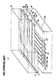
- FIG 7 is a perspective exploded view showing a schematic structure of a conventional AC driving surface discharge type of Plasma Display Panel (hereinafter referred to as PDP) 1 in which a part of the front insulation substrate 2 is cut out.
- PDP Plasma Display Panel
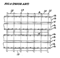
- Figure 8 is a top view showing a state in which a front insulation substrate 2 of the PDP 1 is removed.
- Figure 9 is an enlarged sectional view showing a section along a line A-A' in Fig. 8.
- the PDP 1 is disclosed in Japanese Patent No. 3036496, Japanese Patent Application Laid-open No. Hei 11-202831, and the like.
- a plurality of pairs of sustaining electrodes 3a and sustaining electrodes 3b each extending in a row direction (in a horizontal direction in Fig. 8) are arranged in a column direction (in a vertical direction in Fig. 8) at predetermined intervals so that a discharge gap 4 is put between each pair.
- the front insulation substrate 2 is made of soda lime glass or the like so as to have a thickness of 2 mm to 5 mm similarly to a back insulation substrate 8 which will be described later.
- Both of the sustaining electrode 3a and the sustaining electrode 3b are made up of transparent conductive thin films such as tin oxide, indium oxide, and ITO (Indium Tin Oxide) and form a surface discharge electrode pair 3.
- a plurality of pairs of bus electrodes 5a and bus electrodes 5b are respectively formed on low surfaces of the plurality of pairs of sustaining electrodes 3a and sustaining electrodes 3b at one side of each end.
- the bus electrodes 5a and the bus electrodes 5b are made up of metal films such as thick films of silver, or thin films of aluminum or copper and are formed in order to make resistance values of the sustaining electrode 3a and the sustaining electrode 3b with a low respective electrical conductivity.
- Respective lower faces on which no sustaining electrode 3a and no sustaining electrode 3b and no bus electrode 5a and no bus electrode 5b are formed in the front insulation substrate 2 are covered by a dielectric layer 6 which is transparent.
- the dielectric layer 6 is made of low melting point glass with a thickness of 10 ⁇ m to 40 ⁇ m.
- a protection layer 7 is formed on the lower face of the dielectric layer 6 in order to protect the dielectric layer 6 from ion impacts during discharge.
- the protection layer 7 is made of magnesium oxide or the like of which a secondary emission coefficient is large and of which a sputtering-resistance is good, and formed by vacuum deposition or the like so as to have a thickness of 0.5 ⁇ m to 2.0 ⁇ m.
- a plurality of data electrodes 9 in stripe shapes extending in a column direction, namely, in a direction perpendicular to the formation direction of the sustaining electrodes 3a and the sustaining electrodes 3b are formed at predetermined intervals.
- the data electrode 9 is made up of a silver film or the like. Respective upper faces of the data electrodes 9 and the back insulation substrate 8 on which no data electrodes 9 are formed are covered by a white dielectric layer 10.
- a plurality of division walls 13 for separating display cells 12 are formed in the column direction.
- the display cell 12 is a minimum unit for forming a display screen. In Fig. 8, an area surrounded by a dashed line indicates one of the display cells 12.
- Three fluorescent layers 14R, 14G, and 14B for converting an ultraviolet ray which is generated by discharge of a discharge gas into three primary colors of red (R), green (G), and blue (B) of a visible light are formed on the upper face of the dielectric layer 8 on the data electrode 9 and on the side face of the division wall 13.
- the fluorescent layers 14R, 14G, and 14B are formed in order of the fluorescent layer 14R, the fluorescent layer 14G, and the fluorescent layer 14B sequentially repeatedly in the row direction.
- the fluorescent layers (not shown) for converting each ultraviolet ray into a visible light of a same color are formed continuously in the column direction.
- Each discharge gas space 15 is kept in each space formed by the lower face of the protection layer 7, each upper face of the fluorescent layers 14R, 14G, and 14B, and two division walls 13 adjacent to each other.
- the discharge gas space 15 is filled with a discharge gas such as xenon, helium, or neon, or mixed gas thereof under pressure of 20 kPa to 80 kPa,
- a discharge gas such as xenon, helium, or neon, or mixed gas thereof under pressure of 20 kPa to 80 kPa
- An area including the sustaining electrode 3a and the sustaining electrode 3b, the bus electrode 5a and the bus electrode 5b, the data electrode 9, the fluorescent layers 14R, 14G, and 14B and the discharge gas space 15 makes the display cell 12.
- the sustaining electrode 3a and the sustaining electrode 3b with widths of 300 ⁇ m to 500 ⁇ m and with thicknesses of 0.1 ⁇ m to 2.0 ⁇ m are made so as to have the discharge gap 4 of 50 ⁇ m to 300 ⁇ m therebetween.
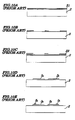
- a method of forming the sustaining electrode 3a and the sustaining electrode 3b, and the bus electrode 5a and the bus electrode 5b included in the PDP 1 will be explained with reference to Fig. 10A to Fig. 10E.
- the sustaining electrode 3a and the sustaining electrode 3b are formed by a lift-off method shown in Fig. 10A to Fig. 10E.
- Figure 10A to Fig. 10E are enlarged sectional views showing a side of the front insulation substrate 2 which is enlaged and is turned over up and down in a section along a line A-A' in Fig. 8.
- a photosensitive dry film 21 is laminated on the front insulation substrate 2.
- the photosensitive dry film 21 includes a support film (not shown) and photosensitive resin (not shown) formed on the support film. Then, as shown in Fig. 10B, the photosensitive dry film 21 is exposed and developed to pattern the dry film 21. Then, as shown in Fig. 10C, a transparent conductive thin film 22 is formed on the photosensitive dry film 21 which is patterned. Then, as shown in Fig. 10D, the sustaining electrode 3a and the sustaining electrode 3b of predetermined shapes are obtained by removing the photosensitive dry film 21. Then, as shown in Fig.
- the bus electrode 5a and the bus electrode 5b of predetermined shapes are obtained by annealing (for example, keeping 560 °C for thirty minutes).
- the generated ultraviolet rays are irradiated to the fluorescent layer 14R, the fluorescent layer 14G, and the fluorescent layer 14B.
- the fluorescent layer 14R, the fluorescent layer 14G, and the fluorescent layer 14B to which the ultraviolet rays are irradiated respectively, generate a visible red light, a visible green light, and a visible blue light.
- the visible red light, the visible green light, and the visible blue are respectively reflected by the white dielectric layer 10, and then go out after passing through the protection layer 7, the dielectric layer 6, the sustaining electrode 3a, the sustaining electrode 3b, and the front insulation substrate 2.
- the discharge which is generated in the diacharge gas space is stopped automatically, after electric charges are accumulated on a lower face of the dielectric layer 6.
- a positive pulse voltage is applied to the sustaining electrode 3a and a negative pulse voltage is applied to the sustaining electrode 3b as voltage signal
- electrons which are generated by the discharge in the discharge gas space 15 move to the sustaining electrode 3a and positive ions such as xenon atoms move to the sustaining electrode 3b.
- the lower face of the dielectric layer 6 formed under the sustaining electrode 3a is negatively charged and the lower face of the dielectric layer 6 formed under the sustaining electrode 3b is positively charged, and then the charge is stopped.
- the discharge current density of the display cell 12 does not change after all, and therefore, the luminous efficiency hardly changes.
- the areas of the sustaining electrode 3a and the sustaining electrode 3b are reduced, the charge does not diffuse in the sustaining electrode 3a and the sustaining. electrode 3b over all, and therefore, only a part of the fluorescent layer 14R, the fluorescent layer 14G, and the fluorescent layer 14B emits. As a result, a luminance of the display cell 12 gets worse, and it is impossible to obtain a sufficient image quality.
- a sustaining electrode made up of a transparent conductive thin film includes a main part extending in a row direction and a projection part projecting from the main part to an adjacent sustaining electrode for each display cell. Then, the projection part has a narrow small part with a width in the row direction which is narrower than a width of a top end part in the row direction. In this technique, the narrow small part is provided, whereby the discharge current for one display cell is reduced so as to reduce the power consumption. As a result, the luminous efficiency is improved.
- the discharge concentrates near the small narrow part and does not diffuse in the display cell over all, there is a possibility that a luminance lowers.
- the sustaining electrode made up of the transparent conductive thin film is patterned in a complex shape, a crack occurs in the small narrow part and there is a possibility of breaking.
- a plasma display panel having a plurality of surface discharge electrode pairs formed in a column direction at predetermined intervals, each of the surface discharge electrode pairs having a pair of sustaining electrodes extending in a row direction so that a discharge gap is put between the sustaining electrodes, wherein:
- a preferable mode is one wherein the sub-electrode is provided with a first parallel portion extending in the row direction at a predetermined distance from the main electrode portion, and a second parallel portion extending in the row direction at a predetermined distance from the first parallel portion between the main electrode portion and the first parallel portion.
- a preferable mode is one wherein the sub-electrode is provided with a vertical portion extending to the main electrode portion at a position at which distances from adjacent division walls extending in the column direction for separating each display cell are approximately equal and integrated with the first parallel portion and the second parallel portion in a manner that an and portion of the vertical portion is electrically in contact with the main electrode portion.
- a preferable mode is one wherein the sub-electrode is provided with a first vertical portion extending to the main electrode portion at a position at which distances from adjacent division walls extending in the column direction for separating each display cell are approximately equal and integrated with the first parallel portion and the second parallel portion in a manner that an end portion of the vertical portion is electrically in contact with the main electrode portion, and a second vertical portion extending to the main electrode portion in the column direction at an upper side of the division wall and integrated with the first parallel portion and the second parallel portion in a manner that an end portion of the second vertical portion is electrically in contact with the main electrode portion.
- a preferable mode is one wherein a width of the second vertical portion is equal to a width of the division wall or is narrower than the width of the division wall.
- a preferable mode is one wherein a width of the second vertical portion is a halt of a width of the division wall or less.
- a preferable mode is one wherein a width of the second parallel portion is 1 ⁇ m to 50 ⁇ m.
- a preferable mode is one wherein a width of the second parallel portion is 1 ⁇ m to 30 ⁇ m.
- a preferable mode is one wherein a width of the first vertical parallel portion is 1 ⁇ m to 50 ⁇ m.
- a preferable mode is one wherein a width of the first vertical parallel portion is 1 ⁇ m to 30 ⁇ m.
- a preferable mode is one wherein the main electrode portion is provided with a main electrode parallel portion extending in the row direction, and a main electrode projection part projecting from the main electrode portion at a side opposite to the discharge gap side of the main electrode portion at a position at which distances from adjacent division walls extending in the column direction to separate each display cell are approximately equal, and the first vertical portion extends to the main electrode portion in the column direction perpendicular to the first parallel portion and the second parallel portion and is integrated with the first parallel portion and the second parallel portion in a manner that an end portion of the first vertical portion is electrically in contact with the main electrode portion which corresponds.
- a preferable mode is one wherein lengths or the main electrode projection part in the row direction and in the column direction are 30 ⁇ m to 60 ⁇ m.
- a preferable mode is one wherein the sub-electrode portion is provided with a first parallel portion extending in the row direction at a predetermined distance from the main electrode portion, a first vertical portion extending to the main electrode portion in the column direction over each division wall extending in the column direction so as to separate each display cell and integrated with the first parallel portion in a manner that an end portion of the first vertical portion is electrically in contact with the main electrode portion, and a cross part including a second vertical portion extending to the main electrode portion in the column direction at a position at which distances from adjacent division walls are approximately equal and an end portion of the second vertical portion reaching near a aide face of the main electrode portion, and second parallel portions respectively extending from an approximate center to the first vertical portions which are adjacent in a manner that an end portion of each of the second parallel portions reaches near the first vertical portions which are adjacent, the cross part integrated with the first vertical portion.
- a preferable mode is one wherein a width of the first vertical portion is equal to a width of the division wall or is narrower than a width of the division wall.
- a preferable mode is one wherein a width of the first vertical portion is half of a width of the division wall or less.
- a preferable mode is one further including:
- a preferable mode is one wherein a width of the main electrode portion is 30 ⁇ m to 100 ⁇ m.
- a preferable mode is one wherein a width of the main electrode portion is 40 ⁇ m to 80 ⁇ m.
- a preferable mode is one wherein widths of the first parallel portion and the second parallel portion are 30 ⁇ m to 100 ⁇ m.
- a preferable mode is one wherein widths of the first parallel portion and the second parallel portion are 40 ⁇ m to 80 ⁇ m.
- a preferable mode is one wherein a width of the first parallel portion is 30 ⁇ m to 60 ⁇ m.
- a preferable mode is one wherein both of an interval between the main electrode portion and the first parallel portion, and an interval between the second parallel portion and the first parallel portion are 30 ⁇ m to 140 ⁇ m.
- a method of manufacturing a plasma display panel according to the first aspect including:
- a method of manufacturing a plasma display panel according to the first aspect including:
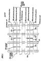
- a plurality of pairs of sustaining electrodes 33a and sustaining electrodes 33b extending in a row direction (in a horizontal direction in Fig. 1) as whole are alternately arranged in a column direction (in a vertical direction in Fig. 1) at predetermined intervals so that a discharge gap 34 is put between each pair.
- the front insulation substrate 32 (shown in Fig. 2A-2F) is made of soda lime glass or the like so as to have a thickness of 2 mm to 5 mm.
- the sustaining electrode 33a and the sustaining electrode 33b form a surface discharge electrode pair 33.
- the sustaining electrode 33a includes a main electrode portion 35a and a sub-electrode portion 36a.
- the sustaining electrode 33b includes a main electrode portion 35b and a sub-electrode portion 36b.
- Both of the main electrode portion 35a and the main electrode portion 35b are made up of transparent conductive thin films in stripe shapes such as tin oxide, indium oxide, or ITO (Indium Tin Oxide). Widths of the main electrode portion 35a and the main electrode portion 35b are from 30 ⁇ m to 100 ⁇ m, preferably, from 40 ⁇ m to 80 ⁇ m.
- a plurality of pairs of the sub-electrode portion 36a and the sub-elactroda portion 36b are respectively formed on lower faces of the plurality of pairs of the main electrode portion 35a and the main electrode portion 35b so as to correspond to the main electrode portion 35a and the main electrode portion 35b.
- the main electrode portion 35a is made up of metal films such as thick films of silver, or thin films of aluminum or copper and are provided with a first parallel portion 37 1 , a second parallel portion 37 2 , and a plurality of vertical portions 37 3 formed for respective display cells 12.
- the first parallel portion 37 1 is formed in parallel with the main electrode portion 35a at a predetermined distance from the main electrode portion 35a so as to extend in the row direction.
- the second parallel portion 37 2 is formed in parallel with the main electrode portion 35a at a predetermined distance from the main electrode portion 35a between the main electrode portion 35a and the first parallel portion 37 1 so as to extend in the row direction.
- Each vertical portion 37 3 is integrated with the first parallel portion 37 1 and the second parallel portion 37 2 , and extends to the main electrode portion 35a in the column direction perpendicular to the first parallel portion 37 1 and the second parallel portion 37 2 , and an upper face of each vertical portion 37 3 is electrically in contact with a lower face of the main electrode portion 35a.
- Each vertical portion 37 3 is formed over a position at which distances from adjacent division walls 13 in the display cell 12 in an area surrounded by a dashed line in Fig. 1 are approximately equal.
- the sub-electrode portion 36b is made up of metal films such as thick films of silver, or thin films of aluminum or copper and are provided with a first parallel portion 38 1 , a second parallel portion 38 2 , and a plurality of vertical portions 38 3 formed fox respective display cells 12.
- the sub-electrode portion 36a and the sub-electrode portion 36b are in a line-symmetric relationship in which a center axis of the discharge gap 34 is used as a symmetry line, and therefore, no detailed explanations of the sub-electrode portion 36b will be given.
- Widths of the first parallel portion 38 1 and the second parallel portion 38 2 are preferably 30 ⁇ m to 60 ⁇ m to reduce resistance values of the main electrode portion 35a and the main electrode portion 35b of which conductivity is low, In other words, the first parallel portion 37 1 and the first parallel portion 38 1 function similarly to conventional bus electrodes. Widths of the second parallel portion 37 2 and the second parallel portion 38 2 , and widths of the vertical portion 37 3 and the vertical portion 38 3 are 1 ⁇ m to 50 ⁇ m, preferably, 1 ⁇ m to 30 ⁇ m. In the first embodiment, both of an interval between the main electrode portion 35a and the second parallel portion 37 2 , and an interval between the second parallel portion 37 2 and the first parallel portion 37 1 are 30 ⁇ m to 140 ⁇ m. Similarly, both of an interval between the main electrode portion 35b and the second parallel portion 38 2 , and an interval between the second parallel portion 38 2 and the first parallel portion 38 1 are 30 ⁇ m to 140 ⁇ m.
- main electrode portion 35a and the main electrode portion 35b, the sub-electrode portion 36a and the sub-electrode portion 36b, and a dielectric layer (not shown) and a protection layer (not shown) which may be sequentially formed on a lower face of the front insulation substrate 32 (shown in Fig.2A-2F) on which no main electrode portion 35a and no main electrode portion 35b,and no sub-electrode portion 36a and no sub-electrode portion 36b are formed are similar to those of a conventional PDP, and therefore, no explanations of those will be given.
- a data electrode, a dielectric layer, a division wall, three kinds of fluorescent layers, and discharge gas to be filled up in a discharge gas space are similar to those of the conventional PDP, and therefore, no explanations of those will be given.
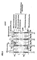
- FIG. 2A to Fig. 2F are enlarged sectional views showing a side of the front insulation substrate 32 which is enlarged and is turned over up and down in a section along a line B-B' in Fig. 1.
- a photosensitive dry film 41 is formed on the front insulation substrate 32.
- the photosensitive dry film 41 includes a support film (not shown) and photosensitive resin (not shown) formed on the support film.
- the photosensitive dry film 41 is exposed and developed to pattern the photosensitive dry film 41.
- a transparent conductive thin film 42 is formed on the photosensitive dry film 41 which is patterned.
- the main electrode portion 35a and the main electrode portion 35b of predetermined shapes ara obtained by removing the photosensitive dry film 41.
- photosensitive silver paste 43 is coated on the front insulation substrate 32 with the main electrode portion 35a and the main electrode portion 35b. Then, as shown in Fig.
- the photosensitive silver paste 43 is exposed and developed, the photosensitive silver paste 43 is patterned, and then annealing is performed (for example, keeping at 550 °C for ten minutes), whereby the sub-electrode portion 36a (shown in Fig.1) first parallel portion 37 1 , the second parallel portion 37 2 and the vertical portion 37 3 , and the sub-electrode portion 36b including the first parallel portion 38 1 , the second parallel portion 38 2 and the vertical portion 38 3 are formed.
- Sheet resistances of the sub-electrode portion 36a and the sub-electrode portion 36b which were formed under the above-mentioned annealing condition were 3 m ⁇ / ⁇ to 4 m ⁇ / ⁇ (Milliohms per Square).
- the vertical portion 37 3 , and the vertical portion 37 4 are not shown in Fig. 2F.
- the main electrode portion 35a and the main electrode portion 35b in stripe shapes are formed so as to extend in the row direction at both sides of the discharge gap 34, discharge becomes stable and a discharge voltage can be reduced.
- the main electrode portion 35a and the main electrode portion 35b are made from transparent conductive thin films, a strong light near the discharge gap 34 can pass through, and a high luminance display can be obtained.
- widths of the main electrode portion 35a and the main electrode portion 35b were set to 30 ⁇ m to 100 ⁇ m, a high luminance display was obtained with stability of the discharge.
- the widths of the main electrode portion 35a and the main electrode portion 35b were set to 40 ⁇ m to 80 ⁇ m, it was possible to reduce the discharge voltage and to obtain a high luminance display.
- the second parallel portion 37 2 and the vertical portion 37 3 are formed between the main electrode portion 35a and the first parallel portion 37 1
- the second parallel portion 38 2 and the vertical portion 38 3 are formed between the main electrode portion 35b and the first parallel portion 38 1 .
- the second parallel portion 37 2 and the second parallel portion 38 2 , and the vertical portion 37 3 and the vertical portion 38 3 are made up of metal films and have a thickness of 1 ⁇ m to 50 ⁇ m. Therefore, according to the structure in the first embodiment, improvement of 10 % to 40 % of the luminous efficiency of the display cell 12 is caused by the following reasons.
- the widths of the second parallel portion 37 2 and the second parallel portion 38 2 , and the widths of the vertical portion 37 1 and the vertical portion 38 3 are set to 1 ⁇ m to 50 ⁇ m, and an aperture is provided for each area between electrode portions forming the sub-electrode portion 36a and the sub-electrode portion 36b, whereby the discharge current density is controlled so as not to be high in those areas.
- the discharge current density is controlled, and this may be the reason why the luminous efficiency of the display cell 12 can be improved.
- the metal film intercepts the visible light, whereas widths of the second parallel portion 37 2 and the second parallel portion 38 2 , and the widths of the vertical portion 37 3 and the vertical portion 38 3 are 1 ⁇ m to 50 ⁇ m. Then, an amount of intercepted visible light is extremely smaller than the whole amount of visible light, and therefore, it does not achieve an amount to influence the luminance.
- the second parallel portion 37 2 and the second parallel portion 38 2 , and the vertical portion 37 3 and the vertical portion 38 are provided, and the widths of them are set to 1 ⁇ m to 50 ⁇ m. Also, there is no case in which areas of the main electrode portion 35a and the main electrode portion 35b are reduced, the shapes of the main electrode portion 35a and the main electrode portion 35b are stripes, and no projection part disclosed in Japanese Patent Application Laid-open No. Hei 8-22772 is provided. According to this structure, the discharge current density is controlled, and the discharge diffuses all over the sustaining electrode 33a and the sustaining electrode 33b. With this structure, since it is possible to excite all of a fluorescent layer 14R, the fluorescent layer 14G, and a fluorescent layer 14B by ultraviolet rays, a luminance of the display cell 12 becomes higher, and a sufficient image quality can be obtained.
- the structure of the first embodiment it is possible to make a higher image quality and to reduce the consumption power.
- the photosensitive silver paste 43 is exposed and developed, and is patterned, and then, annealing is performed. Then, the sub-electrode portion 36a including the first parallel portion 37 1 , the second parallel portion 37 2 , and the vertical portion 37 3 , and the sub-electrode portion 36b including the first parallel portion 38 1 , the second parallel portion 38 2 , and the vertical portion 38 3 , which require a high patterning accuracy, are formed.
- the solution in the exposure is influenced by a thickness of a film, and the transparent conductive film is patterned by using a photosensitive dry film having an insufficient patterning accuracy, it is possible to form the sub-electrode 36a and the sub-electrode 36b easily with a good patterning accuracy.
- the main electrode portion 35a and the main electrode portion 35b are patterned by using a photosensitive dry film for hich the process cost is cheaper.
- the widths of the main electrode portion 35a and the main electrode portion 35b are 30 ⁇ m to 100 ⁇ m, a patterning accuracy is rougher than that of the sub-electrode 36a and the sub-electrode 36b, and therefore, it is possible to pattern the main electrode portion 35a and the main electrode portion 35b cheaply and easily.
- the sub-electrode portion 36a and the sub-electrode portion 36b are made from a metal film, it is hard for a crack to occur at a joint point of the main electrode portion 35a and the vertical portion 37 3 or at an intersection of the first parallel portion 37 1 and the vertical portion 37 3 and it is hard to break a wire.
- a plurality of pairs of sustaining electrodes 53a and sustaining electrodes 53b extending in a row direction (in a horizontal direction in Fig. 3) as whole are alternately arranged in a column direction (in a vertical direction in Fig. 3) at predetermined intervals so that a discharge gap 54 is put between each pair.
- the front insulation substrate 52 is made of soda lime glass or the like so as to have a thickness of 2 mm to 5 mm.
- the sustaining electrode 53a and the sustaining electrode 53b form a surface discharge electrode pair 53,
- the sustaining electrode 53a includes a main electrode portion 55a and a sub-electrode portion 56a.
- the sustaining electrode 53b includes a main electrode portion 55b and a sub-electrode portion 56b.
- Both of the main electrode portion 55a and the main electrode portion 55b are made up of transparent conductive thin films in stripe shapes such as tin oxide, indium oxide, or ITO (Indium Tin Oxide). Widths of the main electrode portion 55a and the main electrode portion 55b are 30 ⁇ m to 100 ⁇ m, preferably 40 ⁇ m to 80 ⁇ m.
- a plurality of pairs of the sub-electrode portion 56a and the sub-electrode portion 56b are respectively formed on lower faces of the plurality of pairs of the main electrode portion 55a and the main electrode portion 55b so as to correspond to the main electrode portion 55a and the main electrode portion 55b.
- the main electrode portion 55a is made up of metal films such as thick films of silver, or thin films of aluminum or copper and is provided with a first parallel portion 57 1 , a second parallel portion 57 2 , a plurality of first vertical portions 57 3 formed for respective display cells 12, and a plurality of second vertical portions 57 4 provided over a division wall 13.
- the first parallel portion 57 1 is formed in parallel with the main electrode portion 55a at a predetermined distance from the main electrode portion 55a so as to extend in the row direction.
- the second parallel portion 57 2 is formed in parallel with the main electrode portion 55a at a predetermined distance from the main electrode 55a between the main electrode portion 55a and the first parallel portion 57 1 so as to extend in the row direction.
- Each first vertical portion 57 3 is integrated with the first parallel portion 57 1 and the second parallel portion 57 2 , and extends to the main electrode portion 55a in the column direction perpendicular to the first parallel portion 57 1 and the second parallel portion 57 2 , and an upper face of each first vertical portion 57 3 is electrically in contact with a lower face of the main electrode portion 35a.
- Each first vertical portion 57 3 is formed over a position at which distances from an adjacent division wall 13 in the display cell 12 in an area surrounded by a dashed line in Fig. 3 are approximately equal.
- Each second vertical portion 57 4 is integrated with the first parallel portion 57 1 and the second parallel portion 57 2 , and extends to the main electrode portion 55a in the column direction perpendicular to the first parallel portion 57 1 and the second parallel portion 57 2 , and an upper face of an end portion of each second vertical portion 57 4 is electrically in contact with a lower face of the main electrode portion 55a.
- each second vertical portion 57 4 is formed over the division wall 13 with a length approximately similar to that of the first vertical portion 57 3 which is adjacent.
- the sub-electrode portion 56b is made up of metal films such as thick films of silver, or thin films of aluminum or copper and is provided with a first parallel portion 58 1 , a second parallel portion 58 2 , a plurality of first vertical portions 58 3 formed for respective display cells 12, and a plurality of second vertical portions 58 4 provided over the division wall 13.
- the auto-electrode portion. 56a and the sub-electrode portion 56b are in a line-symmetric relationship in which a center axis of the discharge gap 54 is used as a symmetry line, and therefore, no detailed explanations of the sub-electrode portion 56b will given.
- Widths of the first parallel portion 58 1 and the second parallel portion 58 2 are preferably 30 ⁇ m to 60 ⁇ m to reduce resistance values of the main electrode portion 55a and the main electrode portion. 55b of which each conductivity is low.
- the first parallel portion 57 1 and the first parallel portion 58 1 function similarly to conventional bus electrodes.
- Widths of the second parallel portion 57 2 and the second parallel portion 58 2 , widths of the first vertical portion 57 3 and the first vertical portion 58 3 , and widths of the second vertical portion 57 4 and the second vertical portion 58 4 are 1 ⁇ m to 50 ⁇ m, preferably, 1 ⁇ m to 30 ⁇ m.
- both of an interval between the main electrode portion 55a and the second parallel portion 57 2 , and an interval between the second parallel portion 57 2 and the first parallel portion 57 1 are 30 ⁇ m to 140 ⁇ m.
- both of an interval between the main electrode portion 55b and the second parallel portion 58 2 , and an interval between the second parallel portion 58 2 and the first parallel portion 58 1 are 30 ⁇ m to 140 ⁇ m.
- the widths of the second vertical portion 57 4 and the second vertical portion 58 4 are equal to a width of the division wall 13 or narrower than the width of the division wall 13 from a point of the luminous efficiency and the luminance.
- main electrode portion 55a and the main electrode portion 55b, the sub-electrode portion 56a and the sub-electrode portion 56b, and a dielectric layer (not shown) and a protection layer (not shown) which may be sequentially formed on a lower face of the front insulation substrate 52 (not shown) on which no main electrode portion 55a and no main electrode portion 55b, and no sub-electrode portion 56a and no sub-electrode portion 56b are formed are similar to those of a conventional PDP, and therefore, no explanations of those will be given.
- a data electrode, a dielectric layer, a division wall, and three kinds of fluorescent layers (all not shown) which are sequentially formed on the back insulation substrate, and discharge gas to be filled up in a discharge gas space are similar to those of the conventional PDP, and therefore, no explanations of those will be given.
- a method of forming the sustaining electrode 53a and the sustaining electrode 53b included in the PDP 51 is approximately similar to that of the first embodiment except for a pattern shape in patterning of a photosensitive silver paste 43 (not shown) since shapes of the sub-electrode portion 56a and the sub-electrode portion 56b are different from those of a sub-electrode portion 36a and a sub-electrode portion 36b. Therefore, no explanations of the method will be given.
- the second vertical portion 57 4 and the second vertical portion 58 4 are above the division wall 13.
- the discharge diffuses near the division wall 13
- xenon atoms or the like excited by the discharge generate ultraviolet rays
- the generated ultraviolet rays are irradiated to side walls (not shown) of the division wall 13 and to a fluorescent layer 14R, a fluorescent layer 14G, and a fluorescent layer 14B (all not shown) which are formed near the side walls.
- the widths of the second vertical portion 57 4 and the second vertical portion 58 4 are equal to that of the division wall 13 or narrower.
- the width of the division wall 13 varies at bottom and top.
- the width of the division wall 13 indicates the top width of the division wall 13.
- the width of the division wall 13 also indicates the top width.
- the widths of the second vertical portion 57 4 and the second vertical portion 58 4 are half of that of the division wall 13 or less.
- Distortions generate in the front insulation substrate (not shown) and the back insulation substrate (not shown) in an annealing process after forming the sustaining electrode 53a and the sustaining electrode 53b. Therefore, when the front insulation substrate and the back insulation substrate axe put together, there is a possibility in that a positional relationship between the front insulation substrate and the back insulation substrate displaces.
- a plurality of pairs of sustaining electrodes 63a and sustaining electrodes 63b extending in a row direction (in a horizontal direction in Fig. 4) as whole are alternately arranged in a column direction (in a vertical direction in Fig. 4) at predetermined intervals so that a discharge gap 64 is put between each pair.
- the front insulation substrate 62 is made of soda lime glass or the like so as to have a thickness of 2 mm to 5 mm.
- the sustaining electrode 63a and the austaining electrode 63b form a surface discharge electrode pair 63.
- the sustaining electrode 63a includes a main electrode portion 65a and a sub-electrode portion 66a.
- the sustaining electrode 63b includes a main electrode portion 65b and a sub-electrode portion 66b.
- Both of the main electrode portion 65a and the main electrode portion 65b are made up of transparent conductive thin films in stripe shapes such as tin oxide, indium oxide, or ITO (Indium Tin Oxide).
- the main electrode portion 65a includes a parallel portion 69 1 , and projection parts 69 2
- the main electrode portion 65b includes a parallel portion 70 1 , and projection parts 70 2 .
- the parallel portion 69 1 and the parallel portion 70 1 are formed so as to extend in the row direction, and widths of the parallel portion 69 1 and the parallel portion 70 1 are 30 ⁇ m to 100 ⁇ m, preferably, 40 ⁇ m to 80 ⁇ m.
- the projection parts 69 2 are formed at an upper position at which distances from adjacent division walls 13 in the display cell 12 shown as a area surrounded by a dashed line in Fig. 4 are approximately equal and are formed so as to project from the parallel portion 69 1 at a side opposite to a side facing the discharge gap 64.
- the projection parts 70 2 are formed at an upper position at which distances from adjacent division walls 13 in the display cell 12 shown as a area surrounded by a dashed line in Fig. 4 are approximately equal and are formed so as to project from the parallel portion 70 1 at a side opposite to a side facing the discharge gap 64.
- both lengths in the row direction and in the column direction are set to 30 ⁇ m to 60 ⁇ m, for example, 50 ⁇ m. Under this condition, it is possible to obtain sufficient electrical contact of the projection parts 69 2 and the projection parts 70 2 , and a vertical portion 68 2 and the vertical portion 70 3 which will be described. Additionally, though the main electrode portion 65a and the main electrode portion 65b are provided with the projection parts 69 2 and the projection parts 70 2 , it is possible to obtain a yield equal to the first embodiment in which a main substrate 35a (shown in Fig.1) and a main substrate 35b (shown in Fig.1) stripe shapes are patterned.
- a plurality of pairs of the sub-electrode portion 66a and the sub-electrode portion 66b are respectively formed on lower faces of the plurality of pairs of the main electrode portions 65a and the main electrode portions 65b so as to correspond the main electrode portions 65a and the main electrode portions 65b.
- the sub-electrode portion 66a is made up of metal films such as thick films of silver, or thin films of aluminum or copper and are provided with a first parallel portion 67 1 , a second parallel portion 67 2 , and a plurality of vertical portions 67 3 formed for respective display cells 12.
- the first parallel portion 67 1 is formed in parallel with the main electrode portion 65a at a predetermined distance from the main electrode portion 65a so as to extend in the row direction.
- the second parallel portion 67 2 is formed in parallel with the main electrode portion 65a at a predetermined distance from the main electrode portion 65a between the main electrode portion 65a and the first parallel portion 67 1 so as to extend in the row direction.
- Each vertical portion 67 3 is integrated with the first parallel portion 67 1 and the second parallel portion 67 2 , and extends to the main electrode portion 65a in the column direction perpendicular to the first parallel portion 67 1 and the second parallel portion 67 2 , and an upper face of an end portion of each vertical portion 67 3 is electrically in contact with a lower face of the projection part 69 2 .
- Each vertical portion 67 3 is formed over a position at which distances from adjacent division wall 13 in the display cell 12 in an area surrounded by a dashed line in Fig. 4 are approximately equal.
- the sub-electrode portion 66b is made up of metal films such as thick films of silver, or thin films of aluminum or copper and are provided with a first parallel portion 68 1 , a second parallel portion 68 2 , and the plurality of vertical portions 68 3 formed for respective display cells 12.
- the sub-electrode portion 66a and the sub-electrode portion 66b are in a line-symmetric relationship in which a center axis of the discharge gap 64 is used as a symmetry line, and therefore, no detailed explanations of the sub-electrode portion 66a will be given.
- Widths of the first parallel portion 67 1 and the first parallel portion 68 2 are preferably 30 ⁇ m to 60 ⁇ m to reduce resistance values of the main electrode portion 65a and the main electrode portion 65b of which conductivity is low.
- the first parallel portion 67 1 and the first parallel portion 68 1 function similarly to conventional bus electrodes.
- Widths of the second parallel portion 67 2 and the second parallel portion 68 2 , and widths of the vertical portion 67 3 and the vertical portion 68 3 are 1 ⁇ m to 50 ⁇ m, preferably, 1 ⁇ m to 30 ⁇ m.
- both of an interval between the parallel portion 69 1 of the main electrode portion 65a and the second parallel portion 67 2 , and an interval between the second parallel portion 67 2 and the first parallel portion 67 1 are 30 ⁇ m to 140 ⁇ m.
- both of an interval between the parallel portion 70 1 of the main electrode portion 65b and the second parallel portion 68 1 , and an interval between the second parallel portion 68 2 and the first parallel portion 68 1 are 30 ⁇ m to 140 ⁇ m.
- main electrode portion 65a and the main electrode portion 65b, the sub-electrode portion 66a and the sub-electrode portion 66b, and a dielectric layer (not shown) and a protection layer (not shown) which may be sequentially formed on a lower face of the front insulation substrate 62 (not shown) on which no main electrode portion 65a and no main electrode portion 65b, and no sub-electrode portion 66a and no sub-electrode portion 66b are formed are similar to those of the conventional PDP, and therefore, no explanations of those will be given.
- a data electrode, a dielectric layer, a division wall, and three kinds of fluorescent layers (all not shown) which are sequentially formed on the back insulation substrate, and discharge gas to be filled up in a discharge gas space are similar to those of the conventional PDP, and therefore, no explanations of those will be given.
- a method of forming the sustaining electrode 63a and the sustaining electrode 63b included in the PDP 61 is approximately similar to that of the first embodiment except for a pattern shape in patterning of a photosensitive dry film 41 (shown in Fig.2A) and a photosensitive silver paste 43 (shown in Fig.
- the main electrode portion 65a is provided with a projection part 69 2 , and each top of the vertical portion 67 3 forming the sub-electrode portion 66a made from the metal film is electrically in contact with only the lower face of the corresponding projection part 69 2 .
- the main electrode portion 65b is provided with the projection part 70 2 , and each top of the vertical portion 68 3 forming the sub-electrode portion 66b made from the metal film is electrically in contact with only the lower face of the corresponding projection part 70 2 . Therefore, according to the structure of the third embodiment since it is possible to reduce the area of the metal film which is not transparent and intercepts visible light, it is possible to make luminance higher and to improve luminous efficiency in comparison with the first embodiment.
- a plurality of pairs of sustaining electrodes 83a and sustaining electrodes 83b extending in a row direction (in a horizontal direction in Fig. 5) as whole are alternately arranged in a column direction (in a vertical direction in Fig. 5) at predetermined intervals so that a discharge gap 84 is put between each pair.
- the front insulation substrate 82 is made at soda lime glass or the like so as to have a thickness of 2 mm to 5 mm.
- the sustaining electrode 83a and the sustaining electrode 83b form a surface discharge electrode pair 83.
- the sustaining electrode 83a includes a main electrode portion 85a and a sub-electrode portion 86a.
- the sustaining electrode 83b includes a main electrode portion 85b and a sub-electrode portion 86b.
- Both of the main electrode portion 85a and the main electrode portion 85b are made up of transparent conductive thin films in stripe shapes such as tin oxide, indium oxide, or ITO (Indium Tin Oxide). Widths of the main electrode portion 85a and the main electrode portion 85b are 30 ⁇ m to 100 ⁇ m, preferably, 40 ⁇ m to 80 ⁇ m. A plurality of pairs of sub-electrode portions 86a and sub-electrode portions 86b are formed at under layers of the main electrode portion 85a and the main electrode portion 85b so as to correspond with the main electrode portion 85a and the main electrode portion 85b.
- the sub-electrode portion 86a is made up of a metal film such as thick film of silver, and a thin film of aluminum, copper or the like, and is provided with a parallel portion 87 1 , a plurality of vertical portions 87 2 provided on a division wall 13, and a plurality of cross parts 87 3 provided for each display cell 12.
- the parallel portion 87 1 is formed in parallel with the main electrode portion 85a at a predetermined distance from the main electrode portion 85a so as to extend in the row direction.
- Each vertical portion 87 2 is integrated with the parallel portion 87 1 and extends in the column direction perpendicular to the parallel portion 87 1 and to the main electrode portion 85a over the division wall 13.
- each vertical portion 87 2 is electrically in contact with the lower face of the main electrode portion 85a.
- Each cross part 87 1 is integrated with the parallel portion 87 1 is formed over a position at which distances from adjacent division wall 13 in the display cell 12 in an area surrounded by a dashed line in Fig. 5 are approximately equal.
- Each cross part 87 3 is provided with a vertical portion 87 3a and a parallel portion 87 3b .
- the vertical portion 87 3a extends to the main electrode 85a in the column direction perpendicular to the parallel portion 87 3b .
- An end of the vertical portion 87 3a reaches near a side face opposite to the side facing the discharge gap 84 of the main electrode portion 85a.
- the parallel portion 87 3b extends from an approximate center to two adjacent vertical portions 87 2 in the row direction and reaches near the side of the vertical portion 87 2 .
- the sub-electrode portion 86b is made up of metal films such as thick films of silver, or thin films of aluminum or copper and is provided with a first parallel portion 88 1 , a plurality of vertical portions 88 2 formed on the division wall 13, a plurality of cross parts 88 3 formed for respective display cells 12.
- the sub-electrode portion 86a and the sub-electrode portion 86b are in a line-symmetric relationship in which a center axis of the discharge gap 84 is used as a symmetry line, and therefore, no detailed explanations of the sub-electrode portion 86b will be given.
- Widths of the parallel portion 87 1 and the parallel portion 88 1 are preferably 30 ⁇ m to 60 ⁇ m to reduce resistance values of the main electrode portion 85a and the main electrode portion 85b of which conductivity is low.
- the parallel portion 87 1 and the first parallel portion 88 1 function similarly to conventional bus electrodes.
- widths of the vertical portion 87 2 and the vertical portion 88 2 are equal to the width of the division wall 13 or narrower than the width of the division wall 13 from points of luminous efficiency and luminance.
- widths of the vertical portion 87 2 and the vertical portion 88 2 are half of the width of the division wall 13 or less from points of manufacturing.
- Widths of the cross part 87 2 and the cross part 88 3 are 1 ⁇ m to 50 ⁇ m, preferably, 1 ⁇ m to 30 ⁇ m. In the fourth embodiment, both of an interval between the main electrode portion 85a and the parallel portion 87 1 , and an interval between the main electrode portion 85b and the parallel portion 88 1 are 60 ⁇ m to 280 ⁇ m.
- main electrode portion 85a and the main electrode portion 85b, the sub-electrode portion 86a and the sub-electrode portion 86b, and a dielectric layer and a protection layer (both not shown) which may be sequentially formed on a lower face of the front insulation substrate 82 (not shown) on which no main electrode portion 85a and no main electrode portion 85b, and no sub-alactrode portion 86a and no sub-electrode portion 86b are formed are similar to those of the conventional PDP, and therefore, no explanations of those will be given.
- a data electrode, a dielectric layer, a division wall, and three kinds of fluorescent layers which are sequentially formed on a back insulation substrate (not shown), and discharge gas to be filled up in a discharge gas space (not shown) are similar to those of a conventional PDP, and therefore, no explanations of those will be given.
- a method of forming the sustaining electrode 83a and the sustaining electrode 83b included in the PDP 81 is approximately similar to that of the first embodiment except for a pattern shape in patterning a photosensitive dry film 41 (shown in fig.2A) and photosensitive silver paste 43 (shown in Fig.2E) since shapes of the sub-electrode portion 86a and the sub-electrode 86b are different from those of a sub-electrode portion 36a (shown in Fig. 1) and a sub-electrode portion 36b (shown in Fig.1). Therefore, no explanations of the method will be given.
- the upper face of the end portion, of the vertical portion 87 3a is not electrically in contact with the lower face of the main electrode 85a, and the end portion of the vertical portion 87 3a is not electrically in contact with the side of the adjacent vertical portion 87 2 . Therefore, according to the structure of the fourth embodiment, since it is possible to reduce an area of metal film which is not transparent and intercepts visible lights in comparison with the second embodiment, it is possible to make luminance higher and to improve luminous efficiency more.
- a plurality of pairs of sustaining electrodes 93a and sustaining electrodes 93b extending in a row direction (in a horizontal direction in Fig. 6) as whole are alternately arranged in a column direction (in a vertical direction in Fig. 6) at predetermined intervals so that a discharge gap 94 is put between each pair.
- the front insulation substrate 92 (not shown) is made of soda lime glass or a like so as to have a thickness of 2 mm to 5 mm.
- the sustaining electrode 93a and the sustaining electrode 93b form a surface discharge electrode pair 93.
- the sustaining electrode 93a includes a main electrode portion 95a and a sub-electrode portion 96a.
- the sustaining electrode 93b includes a main electrode portion 95b and a sub-electrode portion 96b.
- Both of the main electrode portion 95a and the main electrode portion 95b are made up of transparent conductive thin films in stripe shapes such as tin oxide, indium oxide, or ITO (Indium Tin Oxide). Widths of the main electrode portion 95a and the main electrode portion 95b are 30 ⁇ m to 100 ⁇ m, preferably, 40 ⁇ m to 80 ⁇ m.
- a plurality of pairs of sub-electrode portions 96a and sub-electrode portions 96b and a plurality of pairs of bus electrode portions 98a and bus electrode portions 98b are formed at under layers of the main electrode portion 95a and the main electrode portion 95b so as to correspond the main electrode portion 95a and the main electrode portion 95b.
- the sub-electrode 96a is made up of a metal film such as thick film of silver, and a thin film of aluminum, copper or the like, and is provided with a first parallel portion 97 1 , a second parallel portion 97 2 , a plurality of vertical portions 97 3 provided for each display cell 12.
- the first parallel portion 97 1 is formed in parallel with the main electrode portion 95a at a predetermined distance from the main electrode portion 95a so as to extend in the row direction.
- the second parallel portion 97 2 is formed between the main electrode portion 95a and the first parallel portion 97 1 in parallel with the main electrode portion 95a at a predetermined distance from the main electrode portion 95a so as to extend in the row direction.
- Each vertical portion 97 3 is integrated with the first parallel portion 97 1 and the second parallel portion 97 2 , and extends in the column direction perpendicular to the first parallel portion 97 2 and the second parallel portion 97 2 .
- Each top of the vertical portion 97 3 is electrically in contact with the lower face of the main electrode portion 95a.
- Each vertical portion 97 3 is formed over a position at which distances from adjacent division walls 13 in the display cell 12 in an area surrounded by a dashed line in Fig. 6 are approximately equal.
- the bus electrode portion 98a is made up of a metal film such as thick film of silver, and a thin film of aluminum, copper or the like, is integrated with the sub-electrode portion 96a, and is provided with a parallel portion 99 1 , and a plurality of vertical portions 99 2 provided over the division wall 13.
- the parallel portion 99 1 is formed in parallel with the first parallel portion 97 1 at a predetermined distance from the first parallel portion 97 1 as not to be influenced by the discharge and so as to extend in the row direction.
- Each vertical portion 99 3 is integrated with the first parallel portion 97 1 , the second parallel portion 97 2 , and the parallel portion 99 1 and extends in the column direction perpendicular to the first parallel portion 97 1 , the second parallel portion 97 2 and the parallel portion 99 1 .
- An upper face of an and portion of each vertical portion 97 2 is electrically in contact with the lower face of the first parallel portion 97 1 .
- the sub-electrode portion 96b is made up of metal films such as thick films of silver, or thin films of aluminum or copper and is provided with a first parallel portion 100 1 , a second parallel portion 100 2 , a plurality of vertical portions 100 3 formed for respective display cells 12.
- the bus electrode portion 98b is made up of metal films such as thick films of silver, or thin films of aluminum or copper, is integrated with the sub-electrode portion 96b and is provided with a parallel portion 101 1 , and a plurality of vertical portions 101 2 formed over the division wall 13.
- the sub-electrode portion 96a and the sub-electrode portion 96b are in a line-symmetric relationship in which a center axis of the discharge gap 94 is used as a symmetry line, and therefore, no detailed explanations of the sub-electrode portion 96b will given.
- bus electrode portion 98a and the bus electrode portion 98b are in a line-symmetric relationship in which a center axis of the discharge gap 94 is used as a symmetry line, and therefore, no detailed explanations of the bus-electrode portion 96b will given.
- Widths of the first parallel portion 97 1 and the first parallel portion 100 1 , widths of the second parallel portion 97 2 and the second parallel portion 100 2 , widths of the vertical portion 97 3 and the vertical portion 100 3 are 1 ⁇ m to 50 ⁇ m, preferably, 1 ⁇ m to 30 ⁇ m.
- both of an interval between the main electrode portion 95a and the second parallel portion 97 2 , and an interval between the second parallel portion 97 2 and the first parallel portion 97 1 are 30 ⁇ m to 140 ⁇ m.
- both of an interval between the main electrode portion 95b and the second parallel portion 100 2 , and an interval between the second parallel portion 100 2 and the first parallel portion 100 1 are 30 ⁇ m to 140 ⁇ m.
- both of an interval between the parallel portion 99 1 and the parallel portion 100 2 , forming the bus electrode portion 98a and the bus electrode portion 98b are preferably 30 ⁇ m to 60 ⁇ m to reduce the resistance values of the main electrode portion 95a and the main electrode portion 95b of which conductivity is low.
- main electrode portion 95a and the main electrode portion 95b, the sub-electrode portion 96a and the sub-electrode portion 96b, the bus electrode portion 98a and the bus electrode portion 98b, and a dielectric layer (not shown) and a protection layer (not shown) which may be sequentially formed on a lower face of the front insulation substrate 92 (not shown) on which no main electrode portion 95a and no main electrode portion 95b, no sub-electrode portion 96a and no sub-electrode portion 96b, and no bus electrode portion 98a and no bus electrode portion 98b are formed are similar to those of a conventional PDP, and therefore, no explanations of those will be given.
- a data electrode, a dielectric layer, a division wall, and three kinds of fluorescent layers (all not shown) which are sequentially formed on the back insulation substrate (not shown), and discharge gas to be filled up in a discharge gas apace (not shown) are similar to those of the conventional PDP, and therefore, no explanations of those will be given.
- a method of forming the sustaining electrode 93a and the sustaining electrode 93b and the bus electrode portion 98a and the bus electrode portion 98b included in the PDP 91 is approximately similar to that of the first embodiment except for a pattern shape in patterning of a photosensitive silver paste 43 (shown in Fig.2E) since shapes of the sub-electrode portion 96a and the sub-electrode 96b are different from those of the sub-electrode portion 36a (shown in Fig.1) and the sub-electrode portion 36b (shown in Fig. 1) and the bus electrode portion 98a and the bus electrode portion 98b are provided. Therefore, no explanations of the method will be given.
- the bus electrode portion 98a and the bus electrode portion 98b are provided, the following effects can be obtained in addition to those of the first embodiment. Since the resistance values of the main electrode portion 95a and the main electrode portion 95b of which each conductivity is low are reduced by the parallel portion 99 1 and the parallel portion 100 1 included in the bus electrode portion 98a and the bus electrode portion 98b, it is unnecessary to reduce the resistance values by the first parallel portion 97 1 and the first parallel portion 100 1 . With this structure, it is unnecessary to make the widths of the first parallel portion 97 1 and the first parallel portion 100 1 larger to diffuse the discharge into the first parallel portion 97 1 and the first parallel portion 100 1 . Therefore, since it is possible to reduce the area of metal film which is not transparent and intercepts visible lights in comparison with the first embodiment, it is possible to make luminance higher and to improve luminous efficiency more.
- the first embodiment shows a method in which the sub-electrode portion 36a and the sub-electrode portion 36b are formed after the main electrode portion 35a and the main electrode portion 35b are formed.
- the present invention is not limited to this, and the main electrode portion, 35a and the main electrode portion 35b may be formed after the sub-electrode portion 36a and the sub-electrode portion 36b are formed.
- Other embodiments are similar to this.
- the first embodiment shows a method in which the sub-electrode portion 36a and the sub-electrode portion 36b are formed by patterning the photosensitive silver paste 43.
- the present invention is not limited to this, and the sub-electrode portion. 36a and the sub-electrode portion 36b (both shown in Fig.1) may be formed by annealing after patterning the photosensitive silver paste 43 (shown in Fig.2E). Other embodiments are similar to this.
- the process can be made simplex and use rate of materials can be more improved than in a case in which the sub-electrode portion 36a and the sub-electrode portion 36b are formed by patterning the photosensitive silver paste 43.
- all embodiments can be converted with one another.
- the bus electrode portion 98a and the bus electrode portion 98b may be integrated with sub-electrode portions in another embodiment.
Landscapes
- Engineering & Computer Science (AREA)
- Physics & Mathematics (AREA)
- Plasma & Fusion (AREA)
- Chemical & Material Sciences (AREA)
- Materials Engineering (AREA)
- Manufacturing & Machinery (AREA)
- Gas-Filled Discharge Tubes (AREA)
Abstract
Description
- The present invention relates to a plasma display panel used as a flat display for a television receiver, a computer, and the like, and a method of manufacturing the plasma display panel (PDP), and more particularly, relates to an AC (Alternating Current) driving surface discharge type of plasma display panel and a method of manufacturing the AC driving surface discharge type of plasma display panel.
- The present application claims priority of Japanese Patent Application No. 2001-191765 filed on June 25, 2001, which is hereby incorporated by reference.
- Figure 7 is a perspective exploded view showing a schematic structure of a conventional AC driving surface discharge type of Plasma Display Panel (hereinafter referred to as PDP) 1 in which a part of the
front insulation substrate 2 is cut out. Figure 8 is a top view showing a state in which afront insulation substrate 2 of thePDP 1 is removed. Figure 9 is an enlarged sectional view showing a section along a line A-A' in Fig. 8. ThePDP 1 is disclosed in Japanese Patent No. 3036496, Japanese Patent Application Laid-open No. Hei 11-202831, and the like. - In the
PDP 1, as shown in Fig. 7 to Fig. 9, under thefront insulation substrate 2, a plurality of pairs of sustaining electrodes 3a and sustainingelectrodes 3b each extending in a row direction (in a horizontal direction in Fig. 8) are arranged in a column direction (in a vertical direction in Fig. 8) at predetermined intervals so that a discharge gap 4 is put between each pair. Thefront insulation substrate 2 is made of soda lime glass or the like so as to have a thickness of 2 mm to 5 mm similarly to aback insulation substrate 8 which will be described later. Both of the sustaining electrode 3a and the sustainingelectrode 3b are made up of transparent conductive thin films such as tin oxide, indium oxide, and ITO (Indium Tin Oxide) and form a surface discharge electrode pair 3. - A plurality of pairs of bus electrodes 5a and
bus electrodes 5b are respectively formed on low surfaces of the plurality of pairs of sustaining electrodes 3a and sustainingelectrodes 3b at one side of each end. The bus electrodes 5a and thebus electrodes 5b are made up of metal films such as thick films of silver, or thin films of aluminum or copper and are formed in order to make resistance values of the sustaining electrode 3a and thesustaining electrode 3b with a low respective electrical conductivity. - Respective lower faces on which no sustaining electrode 3a and no sustaining
electrode 3b and no bus electrode 5a and nobus electrode 5b are formed in thefront insulation substrate 2 are covered by a dielectric layer 6 which is transparent. The dielectric layer 6 is made of low melting point glass with a thickness of 10 µm to 40 µm. A protection layer 7 is formed on the lower face of the dielectric layer 6 in order to protect the dielectric layer 6 from ion impacts during discharge. The protection layer 7 is made of magnesium oxide or the like of which a secondary emission coefficient is large and of which a sputtering-resistance is good, and formed by vacuum deposition or the like so as to have a thickness of 0.5 µm to 2.0 µm. - On the other hand, a plurality of
data electrodes 9 in stripe shapes extending in a column direction, namely, in a direction perpendicular to the formation direction of the sustaining electrodes 3a and thesustaining electrodes 3b are formed at predetermined intervals. Thedata electrode 9 is made up of a silver film or the like. Respective upper faces of thedata electrodes 9 and theback insulation substrate 8 on which nodata electrodes 9 are formed are covered by a whitedielectric layer 10. On thedielectric layer 9 except thedata electrode 9, a plurality ofdivision walls 13 for separatingdisplay cells 12 are formed in the column direction. Thedisplay cell 12 is a minimum unit for forming a display screen. In Fig. 8, an area surrounded by a dashed line indicates one of thedisplay cells 12. - Three
fluorescent layers dielectric layer 8 on thedata electrode 9 and on the side face of thedivision wall 13. Thefluorescent layers fluorescent layer 14R, thefluorescent layer 14G, and thefluorescent layer 14B sequentially repeatedly in the row direction. The fluorescent layers (not shown) for converting each ultraviolet ray into a visible light of a same color are formed continuously in the column direction. - Each
discharge gas space 15 is kept in each space formed by the lower face of the protection layer 7, each upper face of thefluorescent layers division walls 13 adjacent to each other. Thedischarge gas space 15 is filled with a discharge gas such as xenon, helium, or neon, or mixed gas thereof under pressure of 20 kPa to 80 kPa, An area including the sustaining electrode 3a and the sustainingelectrode 3b, the bus electrode 5a and thebus electrode 5b, thedata electrode 9, thefluorescent layers discharge gas space 15 makes thedisplay cell 12. When the size of thedisplay cell 12 is 1.05 mm in the vertical direction (column direction) and 0.355 mm in the horizontal direction (row direction), the sustaining electrode 3a and thesustaining electrode 3b with widths of 300 µm to 500 µm and with thicknesses of 0.1 µm to 2.0 µm are made so as to have the discharge gap 4 of 50 µm to 300 µm therebetween. - Next, a method of forming the sustaining electrode 3a and the sustaining
electrode 3b, and the bus electrode 5a and thebus electrode 5b included in thePDP 1 will be explained with reference to Fig. 10A to Fig. 10E. The sustaining electrode 3a and the sustainingelectrode 3b are formed by a lift-off method shown in Fig. 10A to Fig. 10E. Figure 10A to Fig. 10E are enlarged sectional views showing a side of thefront insulation substrate 2 which is enlaged and is turned over up and down in a section along a line A-A' in Fig. 8. First, as shown in Fig. 10A, a photosensitivedry film 21 is laminated on thefront insulation substrate 2. The photosensitivedry film 21 includes a support film (not shown) and photosensitive resin (not shown) formed on the support film. Then, as shown in Fig. 10B, the photosensitivedry film 21 is exposed and developed to pattern thedry film 21. Then, as shown in Fig. 10C, a transparent conductive thin film 22 is formed on the photosensitivedry film 21 which is patterned. Then, as shown in Fig. 10D, the sustaining electrode 3a and the sustainingelectrode 3b of predetermined shapes are obtained by removing the photosensitivedry film 21. Then, as shown in Fig. 10E, after pattern printing of silver paste (not shown) is applied onto the sustaining electrode 3a and the sustainingelectrode 3b, the bus electrode 5a and thebus electrode 5b of predetermined shapes are obtained by annealing (for example, keeping 560 °C for thirty minutes). - Now, an outline principle in which one
display cell 12 emits in thePDP 1 will be explained. First, when a voltage signal for keeping discharge is applied to the sustaining electrode 3a and thesustaining electrode 3b, a discharge generates in thedischarge gas space 15. Electrons which are generated by this discharge are in collision with xenon atoms, helium atoms, neon atoms, or the like (hereunder, called only xenon atoms or the like), the xenon atoms or the like are excited or ionized. For example, excited xenon atoms generate ultraviolet rays of a vacuum ultraviolet area of 147 nm to 190 nm. The generated ultraviolet rays are irradiated to thefluorescent layer 14R, thefluorescent layer 14G, and thefluorescent layer 14B. Thefluorescent layer 14R, thefluorescent layer 14G, and thefluorescent layer 14B to which the ultraviolet rays are irradiated respectively, generate a visible red light, a visible green light, and a visible blue light. The visible red light, the visible green light, and the visible blue are respectively reflected by the whitedielectric layer 10, and then go out after passing through the protection layer 7, the dielectric layer 6, the sustaining electrode 3a, thesustaining electrode 3b, and thefront insulation substrate 2. - On the other hand, the discharge which is generated in the diacharge gas space is stopped automatically, after electric charges are accumulated on a lower face of the dielectric layer 6. For example, when a positive pulse voltage is applied to the sustaining electrode 3a and a negative pulse voltage is applied to the sustaining
electrode 3b as voltage signal, electrons which are generated by the discharge in thedischarge gas space 15 move to the sustaining electrode 3a and positive ions such as xenon atoms move to thesustaining electrode 3b. With these processes, the lower face of the dielectric layer 6 formed under the sustaining electrode 3a is negatively charged and the lower face of the dielectric layer 6 formed under the sustainingelectrode 3b is positively charged, and then the charge is stopped. - Recently, concerning general displays, also concerning an AC driving surface discharge type of PDP, it is required that an image quality is high and a power consumption is low.
- However, in the
conventional PDP 1, when a luminance is made high by increasing the voltage to be applied the sustaining electrode 3a and the sustainingelectrode 3b in order to improve the image quality, the power consumption caused by the discharge increases. - Then, to carry out a high image quality and a low power consumption, though a first technique to a third technique are considered, new problems occur as follows.
- First, to reduce the power consumption of the AC driving surface discharge type of PDP, it is necessary to improve a luminous efficiency of a display cell and to reduce a power consumed by the discharge. Generally, in the AC driving surface discharge type of PDP, as a discharge current density becomes low, a luminous efficiency of ultraviolet rays becomes high. As a result, a luminous efficiency of visible light tends to become high. Then, when a voltage to be applied to a sustaining electrode is reduced and a discharge current is reduced, the discharge current density becomes low. Therefore, it is possible to make a luminous efficiency of a display cell high. However, when the voltage to be applied to the sustaining electrode is reduced, the discharge becomes unstable, and therefore, it is impossible to carry out a stable display operation.
- Secondly, when widths of the sustaining electrode 3a and the sustaining
electrode 3b aro made narrow and areas of the sustaining electrode 3a and the sustainingelectrode 3b are reduced, it is possible to reduce a capacitance between the lower face of the dielectric layer 6, and the sustaining electrode 3a and the sustainingelectrode 3b. When a voltage applied to the sustaining electrode 3a is equal to a voltage applied to the sustainingelectrode 3b, a charge amount accumulated on the lower face of the dielectric layar 6 is reduced when the charge is stopped. Therefore, it is possible to reduce a discharge current. However, in the second technique, as described above, since the areas of the sustaining electrode 3a and the sustainingelectrode 3b are reduced, the discharge current density of thedisplay cell 12 does not change after all, and therefore, the luminous efficiency hardly changes. Also, when the areas of the sustaining electrode 3a and the sustainingelectrode 3b are reduced, the charge does not diffuse in the sustaining electrode 3a and the sustaining.electrode 3b over all, and therefore, only a part of thefluorescent layer 14R, thefluorescent layer 14G, and thefluorescent layer 14B emits. As a result, a luminance of thedisplay cell 12 gets worse, and it is impossible to obtain a sufficient image quality. - Thirdly, Japanese Patent Application Laid-open No. Hei 8-22772 discloses the following technique. In this technique, a sustaining electrode made up of a transparent conductive thin film includes a main part extending in a row direction and a projection part projecting from the main part to an adjacent sustaining electrode for each display cell. Then, the projection part has a narrow small part with a width in the row direction which is narrower than a width of a top end part in the row direction. In this technique, the narrow small part is provided, whereby the discharge current for one display cell is reduced so as to reduce the power consumption. As a result, the luminous efficiency is improved. However, in this technique, since the discharge concentrates near the small narrow part and does not diffuse in the display cell over all, there is a possibility that a luminance lowers. Also, in this technique, the sustaining electrode made up of the transparent conductive thin film is patterned in a complex shape, a crack occurs in the small narrow part and there is a possibility of breaking.
- In view of the above, it is an object of the present invention to provide a plasma display panel and a method of manufacturing the plasma display panel capable of providing both a high image quality and a low power consumption.
- According to a first aspect of the present invention, there is provided a plasma display panel having a plurality of surface discharge electrode pairs formed in a column direction at predetermined intervals, each of the surface discharge electrode pairs having a pair of sustaining electrodes extending in a row direction so that a discharge gap is put between the sustaining electrodes, wherein:
- each of the sustaining electrodes is made up of a transparent conductive thin film, is provided with a main electrode portion formed in stripe shapes so as to face the discharge gap and a metal film with a width which is narrower than a width of the main electrode portion, and a sub-electrode formed at a side opposite to the discharge gap side of the main electrode portion which corresponds.
-
- In the foregoing, a preferable mode is one wherein the sub-electrode is provided with a first parallel portion extending in the row direction at a predetermined distance from the main electrode portion, and a second parallel portion extending in the row direction at a predetermined distance from the first parallel portion between the main electrode portion and the first parallel portion.
- Also, a preferable mode is one wherein the sub-electrode is provided with a vertical portion extending to the main electrode portion at a position at which distances from adjacent division walls extending in the column direction for separating each display cell are approximately equal and integrated with the first parallel portion and the second parallel portion in a manner that an and portion of the vertical portion is electrically in contact with the main electrode portion.
- Also, a preferable mode is one wherein the sub-electrode is provided with a first vertical portion extending to the main electrode portion at a position at which distances from adjacent division walls extending in the column direction for separating each display cell are approximately equal and integrated with the first parallel portion and the second parallel portion in a manner that an end portion of the vertical portion is electrically in contact with the main electrode portion, and a second vertical portion extending to the main electrode portion in the column direction at an upper side of the division wall and integrated with the first parallel portion and the second parallel portion in a manner that an end portion of the second vertical portion is electrically in contact with the main electrode portion.
- Also, a preferable mode is one wherein a width of the second vertical portion is equal to a width of the division wall or is narrower than the width of the division wall.
- Also, a preferable mode is one wherein a width of the second vertical portion is a halt of a width of the division wall or less.
- Also, a preferable mode is one wherein a width of the second parallel portion is 1 µm to 50 µm.
- Also, a preferable mode is one wherein a width of the second parallel portion is 1 µm to 30 µm.
- Also, a preferable mode is one wherein a width of the first vertical parallel portion is 1 µm to 50 µm.
- Also, a preferable mode is one wherein a width of the first vertical parallel portion is 1 µm to 30 µm.
- Also, a preferable mode is one wherein the main electrode portion is provided with a main electrode parallel portion extending in the row direction, and a main electrode projection part projecting from the main electrode portion at a side opposite to the discharge gap side of the main electrode portion at a position at which distances from adjacent division walls extending in the column direction to separate each display cell are approximately equal, and the first vertical portion extends to the main electrode portion in the column direction perpendicular to the first parallel portion and the second parallel portion and is integrated with the first parallel portion and the second parallel portion in a manner that an end portion of the first vertical portion is electrically in contact with the main electrode portion which corresponds.
- Also, a preferable mode is one wherein lengths or the main electrode projection part in the row direction and in the column direction are 30 µm to 60 µm.
- Also, a preferable mode is one wherein the sub-electrode portion is provided with a first parallel portion extending in the row direction at a predetermined distance from the main electrode portion, a first vertical portion extending to the main electrode portion in the column direction over each division wall extending in the column direction so as to separate each display cell and integrated with the first parallel portion in a manner that an end portion of the first vertical portion is electrically in contact with the main electrode portion, and a cross part including a second vertical portion extending to the main electrode portion in the column direction at a position at which distances from adjacent division walls are approximately equal and an end portion of the second vertical portion reaching near a aide face of the main electrode portion, and second parallel portions respectively extending from an approximate center to the first vertical portions which are adjacent in a manner that an end portion of each of the second parallel portions reaches near the first vertical portions which are adjacent, the cross part integrated with the first vertical portion.
- Also, a preferable mode is one wherein a width of the first vertical portion is equal to a width of the division wall or is narrower than a width of the division wall.
- Also, a preferable mode is one wherein a width of the first vertical portion is half of a width of the division wall or less.
- Also, a preferable mode is one further including:
- a bus electrode portion including a bus electrode parallel portion extending in the row direction in parallel with the first parallel portion at a distance at which there is no influence from the first parallel portion, and a bus electrode vertical portion extending to the first parallel portion in the column direction perpendicular to the first parallel portion and the bus parallel portion in a manner that an end portion of the bus electrode vertical portion is electrically in contact with the first parallel portion, and the bus electrode portion is integrated with the sub-electrode portion.
-
- Also, a preferable mode is one wherein a width of the main electrode portion is 30 µm to 100 µm.
- Also, a preferable mode is one wherein a width of the main electrode portion is 40 µm to 80 µm.
- Also, a preferable mode is one wherein widths of the first parallel portion and the second parallel portion are 30 µm to 100 µm.
- Also, a preferable mode is one wherein widths of the first parallel portion and the second parallel portion are 40 µm to 80 µm.
- Also, a preferable mode is one wherein a width of the first parallel portion is 30 µm to 60 µm.
- Furthermore, a preferable mode is one wherein both of an interval between the main electrode portion and the first parallel portion, and an interval between the second parallel portion and the first parallel portion are 30 µm to 140 µm.
- According to a second aspect of the present invention, there is provided a method of manufacturing a plasma display panel according to the first aspect, the method including:
- a first step of coating photosensitive silver paste on a front insulation substrate or a front insulation substrate after forming a plurality of surface discharge pair; and
- a second step of forming a sub-electrode portion by annealing after exposing and developing the photosensitive silver paste and patterning the photosensitive silver paste.
-
- According to a third aspect of the present invention, there is provided a method of manufacturing a plasma display panel according to the first aspect, the method including:
- a first step of coating silver paste on a front insulation substrate or a front insulation substrate after forming a plurality of surface discharge pair; and
- a second step of forming the sub-electrode portion by annealing after patterning the silver paste.
-
- With this configuration, it is possible to obtain a high image quality high and to reduce power consumption.
- The above and other objects, advantages, and features of the present invention will be more apparent from the following description taken in conjunction with the accompanying drawings in which:
- Fig. 1 is a top view showing an AC driving surface discharge
type of
PDP 31 in which afront insulation substrate 32 is not shown, according to a first embodiment of the present invention; - Fig. 2A to Fig. 2F are process views for explaining a forming
method of a sustaining electrode 33a and a sustaining electrode
33b of the
PDP 31; - Fig. 3 is a top view showing an AC driving surface discharge
type of PDP 51 in which a
front insulation substrate 52 is not shown, according to a second embodiment of the present invention, - Fig. 4 is a top view showing an AC driving surface discharge type of PDP 61 in which a front insulation substrate 62 is not shown, according to a third embodiment of the present invention;
- Fig. 5 is a top view showing an AC driving surface discharge type of PDP 81 in which a front insulation substrate 82 is not shown according to a fourth embodiment of the present invention;
- Fig. 6 is a top view showing an AC driving surface discharge
type of
PDP 91 in which a front insulation substrate 92 is not shown, according to a fifth embodiment of the present invention; - Fig. 7 is a perspective exploded view showing a schematic
structure of a conventional AC driving surface discharge type of
PDP 1 in which a part of afront insulation substrate 2 is cut out; - Fig. 8 is a top view showing the conventional AC driving
surface discharge type of
PDP 1 in which thefront insulation substrate 2 is not shown; - Fig. 9 is an enlarged sectional view showing a section taken along a line A-A' in Fig. 8; and
- Fig. 10A to Fig. 10E are conventional process views for
explaining a method of forming a sustaining electrode 3a, a
sustaining
electrode 3b, a bus electrode 5a, and abus electrode 5b of thePDP 1. -
- Best modes for carrying out the present invention will be described in further detail using embodiments with reference to the accompanying drawings.
- A first embodiment of the present invention will be described.
- In the
PDP 31, under thefront insulation substrate 32, as shown in Fig. 1, a plurality of pairs of sustaining electrodes 33a and sustaining electrodes 33b extending in a row direction (in a horizontal direction in Fig. 1) as whole are alternately arranged in a column direction (in a vertical direction in Fig. 1) at predetermined intervals so that adischarge gap 34 is put between each pair. The front insulation substrate 32 (shown in Fig. 2A-2F) is made of soda lime glass or the like so as to have a thickness of 2 mm to 5 mm. The sustaining electrode 33a and the sustaining electrode 33b form a surfacedischarge electrode pair 33. The sustaining electrode 33a includes amain electrode portion 35a and a sub-electrode portion 36a. Similarly, the sustaining electrode 33b includes amain electrode portion 35b and a sub-electrode portion 36b. - Both of the
main electrode portion 35a and themain electrode portion 35b are made up of transparent conductive thin films in stripe shapes such as tin oxide, indium oxide, or ITO (Indium Tin Oxide). Widths of themain electrode portion 35a and themain electrode portion 35b are from 30 µm to 100 µm, preferably, from 40 µm to 80 µm. - A plurality of pairs of the sub-electrode portion 36a and the sub-elactroda portion 36b are respectively formed on lower faces of the plurality of pairs of the
main electrode portion 35a and themain electrode portion 35b so as to correspond to themain electrode portion 35a and themain electrode portion 35b. Themain electrode portion 35a is made up of metal films such as thick films of silver, or thin films of aluminum or copper and are provided with a firstparallel portion 371, a secondparallel portion 372, and a plurality ofvertical portions 373 formed forrespective display cells 12. The firstparallel portion 371 is formed in parallel with themain electrode portion 35a at a predetermined distance from themain electrode portion 35a so as to extend in the row direction. The secondparallel portion 372 is formed in parallel with themain electrode portion 35a at a predetermined distance from themain electrode portion 35a between themain electrode portion 35a and the firstparallel portion 371 so as to extend in the row direction. Eachvertical portion 373 is integrated with the firstparallel portion 371 and the secondparallel portion 372, and extends to themain electrode portion 35a in the column direction perpendicular to the firstparallel portion 371 and the secondparallel portion 372, and an upper face of eachvertical portion 373 is electrically in contact with a lower face of themain electrode portion 35a. Eachvertical portion 373 is formed over a position at which distances fromadjacent division walls 13 in thedisplay cell 12 in an area surrounded by a dashed line in Fig. 1 are approximately equal. Similarly, the sub-electrode portion 36b is made up of metal films such as thick films of silver, or thin films of aluminum or copper and are provided with a firstparallel portion 381, a secondparallel portion 382, and a plurality ofvertical portions 383 formed foxrespective display cells 12. The sub-electrode portion 36a and the sub-electrode portion 36b are in a line-symmetric relationship in which a center axis of thedischarge gap 34 is used as a symmetry line, and therefore, no detailed explanations of the sub-electrode portion 36b will be given. - Widths of the first
parallel portion 381 and the secondparallel portion 382 are preferably 30 µm to 60 µm to reduce resistance values of themain electrode portion 35a and themain electrode portion 35b of which conductivity is low, In other words, the firstparallel portion 371 and the firstparallel portion 381 function similarly to conventional bus electrodes. Widths of the secondparallel portion 372 and the secondparallel portion 382, and widths of thevertical portion 373 and thevertical portion 383 are 1 µm to 50 µm, preferably, 1 µm to 30 µm. In the first embodiment, both of an interval between themain electrode portion 35a and the secondparallel portion 372, and an interval between the secondparallel portion 372 and the firstparallel portion 371 are 30 µm to 140 µm. Similarly, both of an interval between themain electrode portion 35b and the secondparallel portion 382, and an interval between the secondparallel portion 382 and the firstparallel portion 381 are 30 µm to 140 µm. - Additionally, the
main electrode portion 35a and themain electrode portion 35b, the sub-electrode portion 36a and the sub-electrode portion 36b, and a dielectric layer (not shown) and a protection layer (not shown) which may be sequentially formed on a lower face of the front insulation substrate 32 (shown in Fig.2A-2F) on which nomain electrode portion 35a and nomain electrode portion 35b,and no sub-electrode portion 36a and no sub-electrode portion 36b are formed are similar to those of a conventional PDP, and therefore, no explanations of those will be given. Also, a data electrode, a dielectric layer, a division wall, three kinds of fluorescent layers, and discharge gas to be filled up in a discharge gas space are similar to those of the conventional PDP, and therefore, no explanations of those will be given. - Next, a method of forming the sustaining electrode 33a and the sustaining electrode 33b included in the
PDP 31 will be explained with reference to Fig. 2A to Fig. 2F. Themain electrode portion 35a and themain electrode portion 35b are formed by a lift-off method shown in Fig. 2A to Fig. 2F. Figure 2A to Fig. 2F are enlarged sectional views showing a side of thefront insulation substrate 32 which is enlarged and is turned over up and down in a section along a line B-B' in Fig. 1. First, as shown in Fig. 2A, a photosensitivedry film 41 is formed on thefront insulation substrate 32. The photosensitivedry film 41 includes a support film (not shown) and photosensitive resin (not shown) formed on the support film. Then, as shown in Fig. 2B, the photosensitivedry film 41 is exposed and developed to pattern the photosensitivedry film 41. - Then, as shown in Fig. 2C, a transparent conductive thin film 42 is formed on the photosensitive
dry film 41 which is patterned. Then, as shown in Fig. 2D, themain electrode portion 35a and themain electrode portion 35b of predetermined shapes ara obtained by removing the photosensitivedry film 41. Then, as shown in Fig. 2E,photosensitive silver paste 43 is coated on thefront insulation substrate 32 with themain electrode portion 35a and themain electrode portion 35b. Then, as shown in Fig. 2F, thephotosensitive silver paste 43 is exposed and developed, thephotosensitive silver paste 43 is patterned, and then annealing is performed (for example, keeping at 550 °C for ten minutes), whereby the sub-electrode portion 36a (shown in Fig.1) firstparallel portion 371, the secondparallel portion 372 and thevertical portion 373, and the sub-electrode portion 36b including the firstparallel portion 381, the secondparallel portion 382 and thevertical portion 383 are formed. Sheet resistances of the sub-electrode portion 36a and the sub-electrode portion 36b which were formed under the above-mentioned annealing condition were 3 mΩ/□ to 4 mΩ/□ (Milliohms per Square). Here, thevertical portion 373, and thevertical portion 374, are not shown in Fig. 2F. As described above, according to the first embodiment, since themain electrode portion 35a and themain electrode portion 35b in stripe shapes are formed so as to extend in the row direction at both sides of thedischarge gap 34, discharge becomes stable and a discharge voltage can be reduced. Also, since themain electrode portion 35a and themain electrode portion 35b are made from transparent conductive thin films, a strong light near thedischarge gap 34 can pass through, and a high luminance display can be obtained. According to an experiment, widths of themain electrode portion 35a and themain electrode portion 35b were set to 30 µm to 100 µm, a high luminance display was obtained with stability of the discharge. Particularly, when the widths of themain electrode portion 35a and themain electrode portion 35b were set to 40 µm to 80 µm, it was possible to reduce the discharge voltage and to obtain a high luminance display. - Also, the second
parallel portion 372 and thevertical portion 373 are formed between themain electrode portion 35a and the firstparallel portion 371, and the secondparallel portion 382 and thevertical portion 383 are formed between themain electrode portion 35b and the firstparallel portion 381. The secondparallel portion 372 and the secondparallel portion 382, and thevertical portion 373 and thevertical portion 383 are made up of metal films and have a thickness of 1 µm to 50 µm. Therefore, according to the structure in the first embodiment, improvement of 10 % to 40 % of the luminous efficiency of thedisplay cell 12 is caused by the following reasons. - As described above, generally, in an AC driving surface discharge type of PDP, as discharge current density is low, the luminous efficiency of the ultraviolet rays is high. As a result, the luminous efficiency of the visible light tends to be high. In the first embodiment, the widths of the second
parallel portion 372 and the secondparallel portion 382, and the widths of thevertical portion 371 and thevertical portion 383, are set to 1 µm to 50 µm, and an aperture is provided for each area between electrode portions forming the sub-electrode portion 36a and the sub-electrode portion 36b, whereby the discharge current density is controlled so as not to be high in those areas. As described above, the discharge current density is controlled, and this may be the reason why the luminous efficiency of thedisplay cell 12 can be improved. The metal film intercepts the visible light, whereas widths of the secondparallel portion 372 and the secondparallel portion 382, and the widths of thevertical portion 373 and thevertical portion 383 are 1 µm to 50 µm. Then, an amount of intercepted visible light is extremely smaller than the whole amount of visible light, and therefore, it does not achieve an amount to influence the luminance. - According to an experiment, when the widths of the second
parallel portion 372 and the secondparallel portion 382, and the widths of thevertical portion 373 and thevertical portion 383 were set to 1 µm to 30 µm, a high luminance display could be obtained. Also, in the structure of the first embodiment, as the voltage to be applied to the sustaining electrode 33a and the sustaining electrode 33b is not reduced, there does not occur danger that the discharge described as the first problem in the Description of Related Art becomes unstable and a stable display operation cannot be performed. - Also, according to the structure of the first embodiment, the second
parallel portion 372 and the secondparallel portion 382, and thevertical portion 373 and thevertical portion 38, are provided, and the widths of them are set to 1 µm to 50 µm. Also, there is no case in which areas of themain electrode portion 35a and themain electrode portion 35b are reduced, the shapes of themain electrode portion 35a and themain electrode portion 35b are stripes, and no projection part disclosed in Japanese Patent Application Laid-open No. Hei 8-22772 is provided. According to this structure, the discharge current density is controlled, and the discharge diffuses all over the sustaining electrode 33a and the sustaining electrode 33b. With this structure, since it is possible to excite all of afluorescent layer 14R, thefluorescent layer 14G, and afluorescent layer 14B by ultraviolet rays, a luminance of thedisplay cell 12 becomes higher, and a sufficient image quality can be obtained. - Therefore, according to the structure of the first embodiment, it is possible to make a higher image quality and to reduce the consumption power.
- Also, according to the structure of the first embodiment, the
photosensitive silver paste 43 is exposed and developed, and is patterned, and then, annealing is performed. Then, the sub-electrode portion 36a including the firstparallel portion 371, the secondparallel portion 372, and thevertical portion 373, and the sub-electrode portion 36b including the firstparallel portion 381, the secondparallel portion 382, and thevertical portion 383, which require a high patterning accuracy, are formed. Therefore, in comparison with the conventional technique in which the solution in the exposure is influenced by a thickness of a film, and the transparent conductive film is patterned by using a photosensitive dry film having an insufficient patterning accuracy, it is possible to form the sub-electrode 36a and the sub-electrode 36b easily with a good patterning accuracy. - On the other hand, according to the structure of the first embodiment, the
main electrode portion 35a and themain electrode portion 35b are patterned by using a photosensitive dry film for hich the process cost is cheaper. However, since the widths of themain electrode portion 35a and themain electrode portion 35b are 30 µm to 100 µm, a patterning accuracy is rougher than that of the sub-electrode 36a and the sub-electrode 36b, and therefore, it is possible to pattern themain electrode portion 35a and themain electrode portion 35b cheaply and easily. - Also, according to the structure of the first embodiment, since the sub-electrode portion 36a and the sub-electrode portion 36b are made from a metal film, it is hard for a crack to occur at a joint point of the
main electrode portion 35a and thevertical portion 373 or at an intersection of the firstparallel portion 371 and thevertical portion 373 and it is hard to break a wire. - A second embodiment of the present invention will be described.
- In the PDP 51, under the front insulation substrate 52 (not shown), as shown in Fig. 3, a plurality of pairs of sustaining electrodes 53a and sustaining electrodes 53b extending in a row direction (in a horizontal direction in Fig. 3) as whole are alternately arranged in a column direction (in a vertical direction in Fig. 3) at predetermined intervals so that a discharge gap 54 is put between each pair. The
front insulation substrate 52 is made of soda lime glass or the like so as to have a thickness of 2 mm to 5 mm. The sustaining electrode 53a and the sustaining electrode 53b form a surface discharge electrode pair 53, The sustaining electrode 53a includes amain electrode portion 55a and asub-electrode portion 56a. Similarly, the sustaining electrode 53b includes amain electrode portion 55b and asub-electrode portion 56b. - Both of the
main electrode portion 55a and themain electrode portion 55b are made up of transparent conductive thin films in stripe shapes such as tin oxide, indium oxide, or ITO (Indium Tin Oxide). Widths of themain electrode portion 55a and themain electrode portion 55b are 30 µm to 100 µm, preferably 40 µm to 80 µm. - A plurality of pairs of the
sub-electrode portion 56a and thesub-electrode portion 56b are respectively formed on lower faces of the plurality of pairs of themain electrode portion 55a and themain electrode portion 55b so as to correspond to themain electrode portion 55a and themain electrode portion 55b. Themain electrode portion 55a is made up of metal films such as thick films of silver, or thin films of aluminum or copper and is provided with a firstparallel portion 571, a secondparallel portion 572, a plurality of firstvertical portions 573 formed forrespective display cells 12, and a plurality of secondvertical portions 574 provided over adivision wall 13. The firstparallel portion 571 is formed in parallel with themain electrode portion 55a at a predetermined distance from themain electrode portion 55a so as to extend in the row direction. The secondparallel portion 572 is formed in parallel with themain electrode portion 55a at a predetermined distance from themain electrode 55a between themain electrode portion 55a and the firstparallel portion 571 so as to extend in the row direction. Each firstvertical portion 573 is integrated with the firstparallel portion 571 and the secondparallel portion 572, and extends to themain electrode portion 55a in the column direction perpendicular to the firstparallel portion 571 and the secondparallel portion 572, and an upper face of each firstvertical portion 573 is electrically in contact with a lower face of themain electrode portion 35a. Each firstvertical portion 573 is formed over a position at which distances from anadjacent division wall 13 in thedisplay cell 12 in an area surrounded by a dashed line in Fig. 3 are approximately equal. Each secondvertical portion 574 is integrated with the firstparallel portion 571 and the secondparallel portion 572, and extends to themain electrode portion 55a in the column direction perpendicular to the firstparallel portion 571 and the secondparallel portion 572, and an upper face of an end portion of each secondvertical portion 574 is electrically in contact with a lower face of themain electrode portion 55a. Also, each secondvertical portion 574 is formed over thedivision wall 13 with a length approximately similar to that of the firstvertical portion 573 which is adjacent. Similarly, thesub-electrode portion 56b is made up of metal films such as thick films of silver, or thin films of aluminum or copper and is provided with a firstparallel portion 581, a secondparallel portion 582, a plurality of firstvertical portions 583 formed forrespective display cells 12, and a plurality of secondvertical portions 584 provided over thedivision wall 13. The auto-electrode portion. 56a and thesub-electrode portion 56b are in a line-symmetric relationship in which a center axis of the discharge gap 54 is used as a symmetry line, and therefore, no detailed explanations of thesub-electrode portion 56b will given. - Widths of the first
parallel portion 581 and the secondparallel portion 582 are preferably 30 µm to 60 µm to reduce resistance values of themain electrode portion 55a and the main electrode portion. 55b of which each conductivity is low. In other words, the firstparallel portion 571 and the firstparallel portion 581 function similarly to conventional bus electrodes. Widths of the secondparallel portion 572 and the secondparallel portion 582, widths of the firstvertical portion 573 and the firstvertical portion 583, and widths of the secondvertical portion 574 and the secondvertical portion 584 are 1 µm to 50 µm, preferably, 1 µm to 30 µm. In the second embodiment, both of an interval between themain electrode portion 55a and the secondparallel portion 572, and an interval between the secondparallel portion 572 and the firstparallel portion 571 are 30 µm to 140 µm. Similarly, both of an interval between themain electrode portion 55b and the secondparallel portion 582, and an interval between the secondparallel portion 582 and the firstparallel portion 581 are 30 µm to 140 µm. It is preferable that the widths of the secondvertical portion 574 and the secondvertical portion 584 are equal to a width of thedivision wall 13 or narrower than the width of thedivision wall 13 from a point of the luminous efficiency and the luminance. - Additionally, the
main electrode portion 55a and themain electrode portion 55b, thesub-electrode portion 56a and thesub-electrode portion 56b, and a dielectric layer (not shown) and a protection layer (not shown) which may be sequentially formed on a lower face of the front insulation substrate 52 (not shown) on which nomain electrode portion 55a and nomain electrode portion 55b, and nosub-electrode portion 56a and nosub-electrode portion 56b are formed are similar to those of a conventional PDP, and therefore, no explanations of those will be given. Also, a data electrode, a dielectric layer, a division wall, and three kinds of fluorescent layers (all not shown) which are sequentially formed on the back insulation substrate, and discharge gas to be filled up in a discharge gas space are similar to those of the conventional PDP, and therefore, no explanations of those will be given. Also, a method of forming the sustaining electrode 53a and the sustaining electrode 53b included in the PDP 51 is approximately similar to that of the first embodiment except for a pattern shape in patterning of a photosensitive silver paste 43 (not shown) since shapes of thesub-electrode portion 56a and thesub-electrode portion 56b are different from those of a sub-electrode portion 36a and a sub-electrode portion 36b. Therefore, no explanations of the method will be given. - As described above, with the second embodiment, the second
vertical portion 574 and the secondvertical portion 584 are above thedivision wall 13. In addition to the effects obtained by the first embodiment, the following effects can be obtained. Since the secondvertical portion 574 and the secondvertical portion 584 are above thedivision wall 13,the discharge diffuses near thedivision wall 13, xenon atoms or the like excited by the discharge generate ultraviolet rays, the generated ultraviolet rays are irradiated to side walls (not shown) of thedivision wall 13 and to afluorescent layer 14R, afluorescent layer 14G, and afluorescent layer 14B (all not shown) which are formed near the side walls. With this structure, it is possible to make the luminance of thedisplay cell 12 higher than that of the first embodiment. - As described above, from points of luminous efficiency and luminance, it is preferable that the widths of the second
vertical portion 574 and the secondvertical portion 584 are equal to that of thedivision wall 13 or narrower. The width of thedivision wall 13 varies at bottom and top. Here, the width of thedivision wall 13 indicates the top width of thedivision wall 13. Hereunder, the width of thedivision wall 13 also indicates the top width. - On the other hand, from points of manufacturing, it is preferable that the widths of the second
vertical portion 574 and the secondvertical portion 584 are half of that of thedivision wall 13 or less. The reasons will be described. Distortions generate in the front insulation substrate (not shown) and the back insulation substrate (not shown) in an annealing process after forming the sustaining electrode 53a and the sustaining electrode 53b. Therefore, when the front insulation substrate and the back insulation substrate axe put together, there is a possibility in that a positional relationship between the front insulation substrate and the back insulation substrate displaces. When a displacement occurs, and the secondvertical portion 574 and the secondvertical portion 584 are formed not over thedivision wall 13 though the secondvertical portion 574 and the secondvertical portion 584 must be formed over thedivision wall 13, the discharge state changes, and a characteristic changes for every POP 51. Also, in a case of displacement, when a strong discharge generates near thedivision wall 13, the xenon atoms or the like excited by the discharge do not generate ultraviolet rays efficiently, and therefore, the luminous efficiency lowers. Then, the widths of the secondvertical petition 574 and the secondvertical portion 584 are half of thedivision wall 13 or less. Therefore, though a displacement of the front insulation substrate and the back insulation substrata occurs, there is no case in which the widths of the secondvertical portion 574 and the secondvertical portion 584 displace from thedivision wall 13 if only the displacement is in the half of thedivision wall 13 in the row direction. With this structure, it is possible to reduce the influences caused by the displacement. - A third embodiment of the present invention will be described.
- In the PDP 61, under the front insulation substrate 62 (not shown), as shown in Fig. 4, a plurality of pairs of sustaining electrodes 63a and sustaining electrodes 63b extending in a row direction (in a horizontal direction in Fig. 4) as whole are alternately arranged in a column direction (in a vertical direction in Fig. 4) at predetermined intervals so that a
discharge gap 64 is put between each pair. The front insulation substrate 62 is made of soda lime glass or the like so as to have a thickness of 2 mm to 5 mm. The sustaining electrode 63a and the austaining electrode 63b form a surfacedischarge electrode pair 63. The sustaining electrode 63a includes a main electrode portion 65a and a sub-electrode portion 66a. Similarly, the sustaining electrode 63b includes a main electrode portion 65b and asub-electrode portion 66b. - Both of the main electrode portion 65a and the main electrode portion 65b are made up of transparent conductive thin films in stripe shapes auch as tin oxide, indium oxide, or ITO (Indium Tin Oxide). The main electrode portion 65a includes a
parallel portion 691, andprojection parts 692, and the main electrode portion 65b includes aparallel portion 701, andprojection parts 702. Theparallel portion 691 and theparallel portion 701 are formed so as to extend in the row direction, and widths of theparallel portion 691 and theparallel portion 701 are 30 µm to 100 µm, preferably, 40 µm to 80 µm. Theprojection parts 692 are formed at an upper position at which distances fromadjacent division walls 13 in thedisplay cell 12 shown as a area surrounded by a dashed line in Fig. 4 are approximately equal and are formed so as to project from theparallel portion 691 at a side opposite to a side facing thedischarge gap 64. Similarly, theprojection parts 702 are formed at an upper position at which distances fromadjacent division walls 13 in thedisplay cell 12 shown as a area surrounded by a dashed line in Fig. 4 are approximately equal and are formed so as to project from theparallel portion 701 at a side opposite to a side facing thedischarge gap 64. As to shapes of theprojection parts 692 and theprojection parts 702, both lengths in the row direction and in the column direction are set to 30 µm to 60 µm, for example, 50 µm. Under this condition, it is possible to obtain sufficient electrical contact of theprojection parts 692 and theprojection parts 702, and a vertical portion 682 and thevertical portion 703 which will be described. Additionally, though the main electrode portion 65a and the main electrode portion 65b are provided with theprojection parts 692 and theprojection parts 702, it is possible to obtain a yield equal to the first embodiment in which amain substrate 35a (shown in Fig.1) and amain substrate 35b (shown in Fig.1) stripe shapes are patterned. - A plurality of pairs of the sub-electrode portion 66a and the
sub-electrode portion 66b are respectively formed on lower faces of the plurality of pairs of the main electrode portions 65a and the main electrode portions 65b so as to correspond the main electrode portions 65a and the main electrode portions 65b. The sub-electrode portion 66a is made up of metal films such as thick films of silver, or thin films of aluminum or copper and are provided with a firstparallel portion 671, a secondparallel portion 672, and a plurality ofvertical portions 673 formed forrespective display cells 12. The firstparallel portion 671 is formed in parallel with the main electrode portion 65a at a predetermined distance from the main electrode portion 65a so as to extend in the row direction. The secondparallel portion 672 is formed in parallel with the main electrode portion 65a at a predetermined distance from the main electrode portion 65a between the main electrode portion 65a and the firstparallel portion 671 so as to extend in the row direction. Eachvertical portion 673 is integrated with the firstparallel portion 671 and the secondparallel portion 672, and extends to the main electrode portion 65a in the column direction perpendicular to the firstparallel portion 671 and the secondparallel portion 672, and an upper face of an end portion of eachvertical portion 673 is electrically in contact with a lower face of theprojection part 692. Eachvertical portion 673 is formed over a position at which distances fromadjacent division wall 13 in thedisplay cell 12 in an area surrounded by a dashed line in Fig. 4 are approximately equal. Similarly, thesub-electrode portion 66b is made up of metal films such as thick films of silver, or thin films of aluminum or copper and are provided with a first parallel portion 681, a second parallel portion 682, and the plurality of vertical portions 683 formed forrespective display cells 12. The sub-electrode portion 66a and thesub-electrode portion 66b are in a line-symmetric relationship in which a center axis of thedischarge gap 64 is used as a symmetry line, and therefore, no detailed explanations of the sub-electrode portion 66a will be given. - Widths of the first
parallel portion 671 and the first parallel portion 682 are preferably 30 µm to 60 µm to reduce resistance values of the main electrode portion 65a and the main electrode portion 65b of which conductivity is low. In other words, the firstparallel portion 671 and the first parallel portion 681 function similarly to conventional bus electrodes. Widths of the secondparallel portion 672 and the second parallel portion 682, and widths of thevertical portion 673 and the vertical portion 683 are 1 µm to 50 µm, preferably, 1 µm to 30 µm. In the third embodiment, both of an interval between theparallel portion 691 of the main electrode portion 65a and the secondparallel portion 672, and an interval between the secondparallel portion 672 and the firstparallel portion 671 are 30 µm to 140 µm. Similarly, both of an interval between theparallel portion 701 of the main electrode portion 65b and the second parallel portion 681, and an interval between the second parallel portion 682 and the first parallel portion 681 are 30 µm to 140 µm. - Additionally, the main electrode portion 65a and the main electrode portion 65b, the sub-electrode portion 66a and the
sub-electrode portion 66b, and a dielectric layer (not shown) and a protection layer (not shown) which may be sequentially formed on a lower face of the front insulation substrate 62 (not shown) on which no main electrode portion 65a and no main electrode portion 65b, and no sub-electrode portion 66a and nosub-electrode portion 66b are formed are similar to those of the conventional PDP, and therefore, no explanations of those will be given. Also, a data electrode, a dielectric layer, a division wall, and three kinds of fluorescent layers (all not shown) which are sequentially formed on the back insulation substrate, and discharge gas to be filled up in a discharge gas space are similar to those of the conventional PDP, and therefore, no explanations of those will be given. Also, a method of forming the sustaining electrode 63a and the sustaining electrode 63b included in the PDP 61 is approximately similar to that of the first embodiment except for a pattern shape in patterning of a photosensitive dry film 41 (shown in Fig.2A) and a photosensitive silver paste 43 (shown in Fig. 2E) since shapes of the main electrode portion 65a and the main electrode 65b, and the sub-electrode portion 66a and thesub-electrode portion 66b are different from those of amain electrode portion 35a (shown in Fig.1) and amain electrode portion 35b(shown in Fig.1) and a sub-electrode portion 36a (shown in Fig.1) and a sub-electrode portion 36b (shown in Fig.1). Therefore, no explanations of the method will be given. - As described above, with the third embodiment, the main electrode portion 65a is provided with a
projection part 692, and each top of thevertical portion 673 forming the sub-electrode portion 66a made from the metal film is electrically in contact with only the lower face of the correspondingprojection part 692. Similarly, the main electrode portion 65b is provided with theprojection part 702, and each top of the vertical portion 683 forming thesub-electrode portion 66b made from the metal film is electrically in contact with only the lower face of the correspondingprojection part 702. Therefore, according to the structure of the third embodiment since it is possible to reduce the area of the metal film which is not transparent and intercepts visible light, it is possible to make luminance higher and to improve luminous efficiency in comparison with the first embodiment. - A fourth embodiment of the present invention will be described.
- In the PDP 81, under the front insulation substrate 82 (not shown), as shown in Fig. 5, a plurality of pairs of sustaining electrodes 83a and sustaining electrodes 83b extending in a row direction (in a horizontal direction in Fig. 5) as whole are alternately arranged in a column direction (in a vertical direction in Fig. 5) at predetermined intervals so that a discharge gap 84 is put between each pair. The front insulation substrate 82 is made at soda lime glass or the like so as to have a thickness of 2 mm to 5 mm. The sustaining electrode 83a and the sustaining electrode 83b form a surface
discharge electrode pair 83. The sustaining electrode 83a includes a main electrode portion 85a and a sub-electrode portion 86a. Similarly, the sustaining electrode 83b includes a main electrode portion 85b and asub-electrode portion 86b. - Both of the main electrode portion 85a and the main electrode portion 85b are made up of transparent conductive thin films in stripe shapes such as tin oxide, indium oxide, or ITO (Indium Tin Oxide). Widths of the main electrode portion 85a and the main electrode portion 85b are 30 µm to 100 µm, preferably, 40 µm to 80 µm. A plurality of pairs of sub-electrode portions 86a and
sub-electrode portions 86b are formed at under layers of the main electrode portion 85a and the main electrode portion 85b so as to correspond with the main electrode portion 85a and the main electrode portion 85b. The sub-electrode portion 86a is made up of a metal film such as thick film of silver, and a thin film of aluminum, copper or the like, and is provided with aparallel portion 871, a plurality ofvertical portions 872 provided on adivision wall 13, and a plurality ofcross parts 873 provided for eachdisplay cell 12. Theparallel portion 871 is formed in parallel with the main electrode portion 85a at a predetermined distance from the main electrode portion 85a so as to extend in the row direction. Eachvertical portion 872 is integrated with theparallel portion 871 and extends in the column direction perpendicular to theparallel portion 871 and to the main electrode portion 85a over thedivision wall 13. An upper faca end portion of eachvertical portion 872 is electrically in contact with the lower face of the main electrode portion 85a. Eachcross part 871 is integrated with theparallel portion 871 is formed over a position at which distances fromadjacent division wall 13 in thedisplay cell 12 in an area surrounded by a dashed line in Fig. 5 are approximately equal. Eachcross part 873 is provided with avertical portion 873a and aparallel portion 873b. Thevertical portion 873a extends to the main electrode 85a in the column direction perpendicular to theparallel portion 873b. An end of thevertical portion 873a reaches near a side face opposite to the side facing the discharge gap 84 of the main electrode portion 85a. Theparallel portion 873b extends from an approximate center to two adjacentvertical portions 872 in the row direction and reaches near the side of thevertical portion 872. Similarly, thesub-electrode portion 86b is made up of metal films such as thick films of silver, or thin films of aluminum or copper and is provided with a firstparallel portion 881, a plurality ofvertical portions 882 formed on thedivision wall 13, a plurality ofcross parts 883 formed forrespective display cells 12. The sub-electrode portion 86a and thesub-electrode portion 86b are in a line-symmetric relationship in which a center axis of the discharge gap 84 is used as a symmetry line, and therefore, no detailed explanations of thesub-electrode portion 86b will be given. - Widths of the
parallel portion 871 and theparallel portion 881 are preferably 30 µm to 60 µm to reduce resistance values of the main electrode portion 85a and the main electrode portion 85b of which conductivity is low. In other words, theparallel portion 871 and the firstparallel portion 881 function similarly to conventional bus electrodes. It is preferable that widths of thevertical portion 872 and thevertical portion 882 are equal to the width of thedivision wall 13 or narrower than the width of thedivision wall 13 from points of luminous efficiency and luminance. And, it is preferable that widths of thevertical portion 872 and thevertical portion 882 are half of the width of thedivision wall 13 or less from points of manufacturing. Widths of thecross part 872 and thecross part 883 are 1 µm to 50 µm, preferably, 1 µm to 30 µm. In the fourth embodiment, both of an interval between the main electrode portion 85a and theparallel portion 871, and an interval between the main electrode portion 85b and theparallel portion 881 are 60 µm to 280 µm. - Additionally, the main electrode portion 85a and the main electrode portion 85b, the sub-electrode portion 86a and the
sub-electrode portion 86b, and a dielectric layer and a protection layer (both not shown) which may be sequentially formed on a lower face of the front insulation substrate 82 (not shown) on which no main electrode portion 85a and no main electrode portion 85b, and no sub-alactrode portion 86a and nosub-electrode portion 86b are formed are similar to those of the conventional PDP, and therefore, no explanations of those will be given. Also, a data electrode, a dielectric layer, a division wall, and three kinds of fluorescent layers (all not shown) which are sequentially formed on a back insulation substrate (not shown), and discharge gas to be filled up in a discharge gas space (not shown) are similar to those of a conventional PDP, and therefore, no explanations of those will be given. Also, a method of forming the sustaining electrode 83a and the sustaining electrode 83b included in the PDP 81 is approximately similar to that of the first embodiment except for a pattern shape in patterning a photosensitive dry film 41 (shown in fig.2A) and photosensitive silver paste 43 (shown in Fig.2E) since shapes of the sub-electrode portion 86a and the sub-electrode 86b are different from those of a sub-electrode portion 36a (shown in Fig. 1) and a sub-electrode portion 36b (shown in Fig.1). Therefore, no explanations of the method will be given. - As described above, with the fourth embodiment, differently from the second embodiment, as to the
cross part 873, the upper face of the end portion, of thevertical portion 873a is not electrically in contact with the lower face of the main electrode 85a, and the end portion of thevertical portion 873a is not electrically in contact with the side of the adjacentvertical portion 872. Therefore, according to the structure of the fourth embodiment, since it is possible to reduce an area of metal film which is not transparent and intercepts visible lights in comparison with the second embodiment, it is possible to make luminance higher and to improve luminous efficiency more. - A fifth embodiment of the present invention will be described.
- In the
PDP 91, under the front insulation substrate 92 (not shown), as shown in Fig. 6, a plurality of pairs of sustaining electrodes 93a and sustaining electrodes 93b extending in a row direction (in a horizontal direction in Fig. 6) as whole are alternately arranged in a column direction (in a vertical direction in Fig. 6) at predetermined intervals so that adischarge gap 94 is put between each pair. The front insulation substrate 92 (not shown) is made of soda lime glass or a like so as to have a thickness of 2 mm to 5 mm. The sustaining electrode 93a and the sustaining electrode 93b form a surfacedischarge electrode pair 93. The sustaining electrode 93a includes amain electrode portion 95a and a sub-electrode portion 96a. Similarly, the sustaining electrode 93b includes a main electrode portion 95b and a sub-electrode portion 96b. - Both of the
main electrode portion 95a and the main electrode portion 95b are made up of transparent conductive thin films in stripe shapes such as tin oxide, indium oxide, or ITO (Indium Tin Oxide). Widths of themain electrode portion 95a and the main electrode portion 95b are 30 µm to 100 µm, preferably, 40 µm to 80 µm. A plurality of pairs of sub-electrode portions 96a and sub-electrode portions 96b and a plurality of pairs of bus electrode portions 98a andbus electrode portions 98b are formed at under layers of themain electrode portion 95a and the main electrode portion 95b so as to correspond themain electrode portion 95a and the main electrode portion 95b. The sub-electrode 96a is made up of a metal film such as thick film of silver, and a thin film of aluminum, copper or the like, and is provided with a firstparallel portion 971, a secondparallel portion 972, a plurality ofvertical portions 973 provided for eachdisplay cell 12. The firstparallel portion 971 is formed in parallel with themain electrode portion 95a at a predetermined distance from themain electrode portion 95a so as to extend in the row direction. The secondparallel portion 972 is formed between themain electrode portion 95a and the firstparallel portion 971 in parallel with themain electrode portion 95a at a predetermined distance from themain electrode portion 95a so as to extend in the row direction. Eachvertical portion 973 is integrated with the firstparallel portion 971 and the secondparallel portion 972, and extends in the column direction perpendicular to the firstparallel portion 972 and the secondparallel portion 972. Each top of thevertical portion 973 is electrically in contact with the lower face of themain electrode portion 95a. Eachvertical portion 973 is formed over a position at which distances fromadjacent division walls 13 in thedisplay cell 12 in an area surrounded by a dashed line in Fig. 6 are approximately equal. Also, the bus electrode portion 98a is made up of a metal film such as thick film of silver, and a thin film of aluminum, copper or the like, is integrated with the sub-electrode portion 96a, and is provided with a parallel portion 991, and a plurality of vertical portions 992 provided over thedivision wall 13. The parallel portion 991 is formed in parallel with the firstparallel portion 971 at a predetermined distance from the firstparallel portion 971 as not to be influenced by the discharge and so as to extend in the row direction. Each vertical portion 993 is integrated with the firstparallel portion 971, the secondparallel portion 972, and the parallel portion 991 and extends in the column direction perpendicular to the firstparallel portion 971, the secondparallel portion 972 and the parallel portion 991. An upper face of an and portion of eachvertical portion 972 is electrically in contact with the lower face of the firstparallel portion 971, Similarly, the sub-electrode portion 96b is made up of metal films such as thick films of silver, or thin films of aluminum or copper and is provided with a firstparallel portion 1001, a secondparallel portion 1002, a plurality ofvertical portions 1003 formed forrespective display cells 12. Also, thebus electrode portion 98b is made up of metal films such as thick films of silver, or thin films of aluminum or copper, is integrated with the sub-electrode portion 96b and is provided with a parallel portion 1011, and a plurality of vertical portions 1012 formed over thedivision wall 13. The sub-electrode portion 96a and the sub-electrode portion 96b are in a line-symmetric relationship in which a center axis of thedischarge gap 94 is used as a symmetry line, and therefore, no detailed explanations of the sub-electrode portion 96b will given. Similarly, the bus electrode portion 98a and thebus electrode portion 98b are in a line-symmetric relationship in which a center axis of thedischarge gap 94 is used as a symmetry line, and therefore, no detailed explanations of the bus-electrode portion 96b will given. - Widths of the first
parallel portion 971 and the firstparallel portion 1001, widths of the secondparallel portion 972 and the secondparallel portion 1002, widths of thevertical portion 973 and thevertical portion 1003 are 1 µm to 50 µm, preferably, 1 µm to 30 µm. In the fifth embodiment, both of an interval between themain electrode portion 95a and the secondparallel portion 972, and an interval between the secondparallel portion 972 and the firstparallel portion 971 are 30 µm to 140 µm. Similarly, both of an interval between the main electrode portion 95b and the secondparallel portion 1002, and an interval between the secondparallel portion 1002 and the firstparallel portion 1001 are 30 µm to 140 µm. Also, both of an interval between the parallel portion 991 and theparallel portion 1002, forming the bus electrode portion 98a and thebus electrode portion 98b are preferably 30 µm to 60 µm to reduce the resistance values of themain electrode portion 95a and the main electrode portion 95b of which conductivity is low. - Additionally, the
main electrode portion 95a and the main electrode portion 95b, the sub-electrode portion 96a and the sub-electrode portion 96b, the bus electrode portion 98a and thebus electrode portion 98b, and a dielectric layer (not shown) and a protection layer (not shown) which may be sequentially formed on a lower face of the front insulation substrate 92 (not shown) on which nomain electrode portion 95a and no main electrode portion 95b, no sub-electrode portion 96a and no sub-electrode portion 96b, and no bus electrode portion 98a and nobus electrode portion 98b are formed are similar to those of a conventional PDP, and therefore, no explanations of those will be given. Also, a data electrode, a dielectric layer, a division wall, and three kinds of fluorescent layers (all not shown) which are sequentially formed on the back insulation substrate (not shown), and discharge gas to be filled up in a discharge gas apace (not shown) are similar to those of the conventional PDP, and therefore, no explanations of those will be given. Also, a method of forming the sustaining electrode 93a and the sustaining electrode 93b and the bus electrode portion 98a and thebus electrode portion 98b included in thePDP 91 is approximately similar to that of the first embodiment except for a pattern shape in patterning of a photosensitive silver paste 43 (shown in Fig.2E) since shapes of the sub-electrode portion 96a and the sub-electrode 96b are different from those of the sub-electrode portion 36a (shown in Fig.1) and the sub-electrode portion 36b (shown in Fig. 1) and the bus electrode portion 98a and thebus electrode portion 98b are provided. Therefore, no explanations of the method will be given. - As described above, with the configuration of the fifth embodiment, since the bus electrode portion 98a and the
bus electrode portion 98b are provided, the following effects can be obtained in addition to those of the first embodiment. Since the resistance values of themain electrode portion 95a and the main electrode portion 95b of which each conductivity is low are reduced by the parallel portion 991 and theparallel portion 1001 included in the bus electrode portion 98a and thebus electrode portion 98b, it is unnecessary to reduce the resistance values by the firstparallel portion 971 and the firstparallel portion 1001. With this structure, it is unnecessary to make the widths of the firstparallel portion 971 and the firstparallel portion 1001 larger to diffuse the discharge into the firstparallel portion 971 and the firstparallel portion 1001. Therefore, since it is possible to reduce the area of metal film which is not transparent and intercepts visible lights in comparison with the first embodiment, it is possible to make luminance higher and to improve luminous efficiency more. - It is thus apparent that the present invention is not limited to the above embodiments but may be changed and modified without departing from the scope and spirit of the invention.
- For example, the first embodiment, as shown in Fig. 2A to Fig. 2F, shows a method in which the sub-electrode portion 36a and the sub-electrode portion 36b are formed after the
main electrode portion 35a and themain electrode portion 35b are formed. The present invention is not limited to this, and the main electrode portion, 35a and themain electrode portion 35b may be formed after the sub-electrode portion 36a and the sub-electrode portion 36b are formed. Other embodiments are similar to this. - Also, the first embodiment shows a method in which the sub-electrode portion 36a and the sub-electrode portion 36b are formed by patterning the
photosensitive silver paste 43. However, the present invention is not limited to this, and the sub-electrode portion. 36a and the sub-electrode portion 36b (both shown in Fig.1) may be formed by annealing after patterning the photosensitive silver paste 43 (shown in Fig.2E). Other embodiments are similar to this. When the sub-electrode portion 36a and the sub-electrode portion 36b are formed by patterning of thephotosensitive silver paste 43, there are advantages in that the process can be made simplex and use rate of materials can be more improved than in a case in which the sub-electrode portion 36a and the sub-electrode portion 36b are formed by patterning thephotosensitive silver paste 43.
Also, if only there is no discrepancy in the object and the structures, all embodiments can be converted with one another. For example, the bus electrode portion 98a and thebus electrode portion 98b may be integrated with sub-electrode portions in another embodiment.
Claims (24)
- A plasma display panel having a plurality of surface discharge electrode pairs (33) formed in a column direction at predetermined intervals, each of said surface discharge electrode pairs (33) having a pair of sustaining electrodes (33a, 33b) extending in a row direction so that a discharge gap (34) is put between said sustaining electrodes (33a, 33b), characterized in that:each of said sustaining electrodes (33a, 33b) is made up of a transparent conductive thin film, is provided with a main electrode portion (35a, 35b) formed in stripe shapes so as to face said discharge gap (34) and a metal film of which a width is narrower than a width of said main electrode portion (35a, 35b), and a sub-electrode portion (36a, 36b) formed at a side opposite to the discharge gap side of said main electrode portion (35a, 35b) to which it corresponds.
- The plasma display panel according to Claim 1, characterized in that said sub-electrode portion (36a, 36b) is provided with a first parallel portion (371, 381, ..) extending in said row direction at a predetermined distance from said main electrode portion (35a, 35b), and a second parallel portion (372, 382, ..) extending in said row direction at a predetermined distance from said first parallel portion (371, 381, ..) between said main electrode portion (35a, 35b) and said first parallel portion (371, 381, ..).
- The plasma display panel according to Claim 2, characterized in that said sub-electrode portion (36a, 36b) is provided with a vertical portion (373, 383, ..) extending to said main electrode portion (35a, 35b) at a position, at which distances from adjacent division walls extending in said column direction for separating each display cell are approximately equal and integrated with said first parallel portion (371, 381, ..) and said second parallel portion (372, 382, ..) in a manner that an end portion of said vertical portion (373, 383, ..) is electrically in contact with said main electrode portion (35a, 35b).
- The plasma display panel according to claim 2, characterized in that said sub-electrode portion (36a, 36b) is provided with a first vertical portion (573, 583, ..) extending to said main electrode portion (35a, 35b) at a position at which distances from adjacent division walls extending in said column direction for separating each display cell are approximately equal and integrated with said first parallel portion (371, 381, ..) and said second parallel portion (372, 382, ..) in a manner that an end portion of said first vertical portion (573, 583, ..) is electrically in contact with said main electrode portion (35a, 35b), and a second vertical portion (574, 584, ..) extending to said main electrode portion (35a, 35b) in said column direction at an upper side of said division wall and integrated with said first parallel portion (371, 381, ..) and said second parallel portion (372, 382, ..) in a manner that an end portion of said second vertical portion (574, 584, ..) is electrically in contact with said main electrode portion (35a, 35b).
- The plasma display panel according to Claim 4, characterized in that said a width of said second vertical portion (574, 584, ..) is equal to a width of said division wall or is narrower than said width of said division wall.
- The plasma display panel according to Claim 4, characterized in that said a width of said second vertical portion (574, 584, ..) is half of a width of said division wall or less.
- The plasma display panel according to any one of Claim 2 to Claim 6, characterized in that said width of said second parallel portion (372, 382, ..) is 1 µm to 50 µm.
- The plasma display panel according to any one of Claim 2 to Claim 6, characterized in that said width of said second parallel portion (372, 382, ..) is 1 µm to 30 µm.
- The plasma display panel according to any one of Claim 4 to Claim 8, characterized in that said width of said first vertical parallel portion is 1 µm to 50 µm.
- The plasma display panel according to any one of Claim 4 to Claim 8, characterized in that said width of said first vertical parallel portion is 1 µm to 30 µm.
- The plasma display panel according to any one or Claim 4 to Claim 10, characterised in that said main electrode portion (35a, 35b) is provided with a main electrode parallel portion extending in said row direction, and a main electrode projection part projecting from said main electrode portion (35a, 35b) at a side opposite to the discharge gap side of said main electrode portion (35a, 35b) at a position at which distances from adjacent division wall extending in said column direction to separate each display cell are approximately equal, and said first vertical portion (573, 583, ..) extends to said main electrode portion (35a, 35b) in said column direction perpendicular to said first parallel portion (371, 381, ..) and said second parallel portion (372, 382, ..) and is integrated with said first parallel portion (371, 381, ..) and said second parallel portion (372, 382, ..) in a manner that an end portion of said first vertical portion (573, 583, ..) is electrically in contact with said main electrode portion (35a, 35b) to which it corresponds.
- The plasma display panel according to Claim 11, characterized in that lengths of said main electrode projection part in said row direction and in said column direction are 30 µm to 60 µm.
- The plasma display panel according to Claim 1, characterized in that said sub-electrode portion (36a, 36b) is provided with a first parallel portion (371, 381, ..) extending in said row direction at a predetermined distance from said main electrode portion (35a, 35b), a first vertical portion (573, 583, ..) extending to said main electrode portion (35a, 35b) in said column direction over each division wall extending in said column direction so as to separate each display cell and integrated with said first parallel portion (371, 381, ..) in a manner that an end portion of said first vertical portion (573, 583, ..) is electrically in contact with said main electrode portion (35a, 35b), and a cross part including a second vertical portion (574, 584, ..) extending to said main electrode portion (35a, 35b) in said column direction at a position at which distances from adjacent division walls are approximately equal and an end portion of said second vertical portion (574, 584, ..) reaching near a side face of said main electrode portion (35a, 35b), and second parallel portions (372, 382, ..) respectively extending from an approximate center to said first vertical portions (573, 583, ..) which are adjacent in a manner that an end portion of each of said second parallel portions (372, 382, ..) reaches near said first vertical portions (573, 583, ..) which are adjacent, said cross part being integrated with said first vertical portion (573, 583, ..).
- The plasma display panel according to Claim 13, characterized in that a width of said first vertical portion (573, 583, ..) is equal to a width of said division wall or is narrower than a width of said division wall.
- The plasma display panel according to Claim 13, characterized in that a width of said first vertical portion (573, 583, ..) is half of the width of said division wall or less.
- The plasma display panel according to any one of Claim 2 to Claim 15, characterized by further comprising:a bus electrode portion comprising a bus electrode parallel portion extending in said row direction in parallel with said first parallel portion (371, 381, ..) at a distance at which there is no influence from said first parallel portion (371, 381, ..), and a bus electrode vertical portion extending to said first parallel portion (371, 381, ..) in said column direction perpendicular to said first parallel portion (371, 381, ..) and said bus parallel portion in a manner that an end portion of said bus electrode vertical portion is electrically in contact with said first parallel portion, (371, 381, ..) and said bus electrode portion is integrated with said sub-electrode portion (36a, 36b).
- The plasma display panel according to any one of Claim 1 to Claim 5, or Claim 8 to Claim 16, characterized in that a width of said main electrode portion (35a, 35b) is 30 µm to 100 µm.
- The plasma display panel according to any one of Claim 1 to Claim 5, or Claim 8 to Claim 16, characterized in that a width of said main electrode portion (35a, 35b) is 40 µm to 80 µm.
- The plasma display panel according to Claim 11, Claim 12 or Claim16, characterized in that widths of said first parallel portion (371, 381, ..) and said second parallel portion (372, 382, ..) are 30 µm to 100 µm.
- The plasma display panel according to Claim 11, Claim 12 or Claim16, characterized in that widths of said first parallel portion (371, 381, ..) and said second parallel portion (372, 382, ..) are 40 µm to 80 µm.
- The plasma display panel according to any one of Claim 2 to Claim 21, characterized in that a width of said first parallel portion (371, 381, ..) is 30 µm to 60 µm.
- The plasma display panel according to any one of Claim 2 to Claim 21, characterized in that both of an interval between said main electrode portion (35a, 35b) and said first parallel portion (371, 381, ..), and an interval between said second parallel portion (372, 382, ..) and said first parallel portion (371, 381, ..) are 30 µm to 140 µm.
- A method of manufacturing a plasma display panel as set forth in any one of Claim 1 to Claim 22, said method comprising:a first step of coating photosensitive silver paste on a front insulation substrate or a front insulation substrate after forming a plurality of surface discharge pair; anda second step of forming said sub-electrode portion (36a, 36b) by annealing after exposing and developing said photosensitive silver paste and patterning said photosensitive silver paste.
- A method of manufacturing a plasma display panel as set forth in any one of Claim 1 to Claim 22, said method comprising:a first step of coating silver paste on a front insulation substrate or a front insulation substrate after forming a plurality of surface discharge pair; anda second step of forming said sub-electrode portion (36a, 36b) by annealing after patterning said photosensitive silver paste.
Applications Claiming Priority (2)
| Application Number | Priority Date | Filing Date | Title |
|---|---|---|---|
| JP2001191765 | 2001-06-25 | ||
| JP2001191765A JP2003007216A (en) | 2001-06-25 | 2001-06-25 | Plasma display panel and manufacturing method therefor |
Publications (2)
| Publication Number | Publication Date |
|---|---|
| EP1271598A2 true EP1271598A2 (en) | 2003-01-02 |
| EP1271598A3 EP1271598A3 (en) | 2005-10-26 |
Family
ID=19030336
Family Applications (1)
| Application Number | Title | Priority Date | Filing Date |
|---|---|---|---|
| EP02090223A Withdrawn EP1271598A3 (en) | 2001-06-25 | 2002-06-25 | Plasma display panel and method of manufacturing the same |
Country Status (4)
| Country | Link |
|---|---|
| US (2) | US6784615B2 (en) |
| EP (1) | EP1271598A3 (en) |
| JP (1) | JP2003007216A (en) |
| KR (1) | KR100483245B1 (en) |
Cited By (4)
| Publication number | Priority date | Publication date | Assignee | Title |
|---|---|---|---|---|
| EP1469501A3 (en) * | 2003-03-25 | 2006-04-19 | LG Electronics Inc. | Plasma display panel |
| EP1530228A3 (en) * | 2003-11-05 | 2006-07-05 | LG Electronics, Inc. | Plasma diplay panel |
| EP1601001A3 (en) * | 2004-05-25 | 2007-10-17 | Samsung SDI Co., Ltd. | Plasma display panel (PDP) |
| CN100399492C (en) * | 2004-05-25 | 2008-07-02 | 三星Sdi株式会社 | plasma display panel |
Families Citing this family (18)
| Publication number | Priority date | Publication date | Assignee | Title |
|---|---|---|---|---|
| US6614182B2 (en) * | 2000-12-28 | 2003-09-02 | Nec Corporation | Plasma display panel |
| JP2003007216A (en) * | 2001-06-25 | 2003-01-10 | Nec Corp | Plasma display panel and manufacturing method therefor |
| KR20050060836A (en) * | 2003-12-17 | 2005-06-22 | 삼성에스디아이 주식회사 | Plasma display panel |
| KR100659052B1 (en) * | 2003-12-23 | 2006-12-21 | 삼성에스디아이 주식회사 | Plasma display panel |
| KR100637148B1 (en) * | 2004-02-18 | 2006-10-20 | 삼성에스디아이 주식회사 | Plasma display panel |
| KR100578924B1 (en) * | 2004-05-28 | 2006-05-11 | 삼성에스디아이 주식회사 | Plasma display panel |
| KR100658740B1 (en) * | 2004-06-18 | 2006-12-15 | 삼성에스디아이 주식회사 | Plasma display panel |
| KR100922747B1 (en) | 2004-06-23 | 2009-10-22 | 삼성에스디아이 주식회사 | Plasma display panel |
| JP2006012661A (en) * | 2004-06-28 | 2006-01-12 | Pioneer Electronic Corp | Plasma display panel |
| KR20060000758A (en) * | 2004-06-29 | 2006-01-06 | 삼성에스디아이 주식회사 | Plasma display panel |
| KR100578972B1 (en) * | 2004-06-30 | 2006-05-12 | 삼성에스디아이 주식회사 | Plasma display panel |
| EP1646065A3 (en) * | 2004-10-11 | 2009-05-06 | LG Electronics Inc. | Plasma display panel and plasma display apparatus comprising electrodes |
| KR100669329B1 (en) * | 2004-11-15 | 2007-01-15 | 삼성에스디아이 주식회사 | Plasma display panel |
| KR20060098936A (en) * | 2005-03-09 | 2006-09-19 | 삼성에스디아이 주식회사 | Plasma display panel |
| KR100719552B1 (en) * | 2005-06-20 | 2007-05-17 | 삼성에스디아이 주식회사 | Plasma display panel |
| KR100696538B1 (en) | 2005-10-05 | 2007-03-19 | 삼성에스디아이 주식회사 | Plasma display panel without transparent electrode |
| KR100762249B1 (en) * | 2006-05-30 | 2007-10-01 | 엘지전자 주식회사 | Plasma display device |
| KR100762251B1 (en) | 2006-05-30 | 2007-10-01 | 엘지전자 주식회사 | Plasma display device |
Family Cites Families (22)
| Publication number | Priority date | Publication date | Assignee | Title |
|---|---|---|---|---|
| JPH0336496A (en) | 1989-06-30 | 1991-02-18 | Toshiba Corp | Refrigerant pipe of heat pump type air conditioner heat exchanger |
| EP0554172B1 (en) * | 1992-01-28 | 1998-04-29 | Fujitsu Limited | Color surface discharge type plasma display device |
| JP3352821B2 (en) | 1994-07-08 | 2002-12-03 | パイオニア株式会社 | Surface discharge type plasma display device |
| JP3686749B2 (en) * | 1997-11-04 | 2005-08-24 | 太陽インキ製造株式会社 | Patterned inorganic fired coating film and method for producing plasma display panel |
| JP3036496B2 (en) | 1997-11-28 | 2000-04-24 | 日本電気株式会社 | Driving method and circuit for plasma display panel and plasma display panel display |
| JP3039500B2 (en) | 1998-01-13 | 2000-05-08 | 日本電気株式会社 | Driving method of plasma display panel |
| JPH11213894A (en) * | 1998-01-23 | 1999-08-06 | Fujitsu Ltd | Plasma display panel |
| JP3661398B2 (en) * | 1998-03-24 | 2005-06-15 | 松下電器産業株式会社 | Plasma display panel |
| DE69935882T2 (en) * | 1998-05-12 | 2007-09-06 | Matsushita Electric Industrial Co., Ltd., Kadoma | Manufacturing method of a plasma discharge display panel |
| JP2000021313A (en) * | 1998-06-30 | 2000-01-21 | Fujitsu Ltd | Plasma display panel |
| JP3838311B2 (en) * | 1998-10-09 | 2006-10-25 | 株式会社日立プラズマパテントライセンシング | Plasma display panel |
| JP2000357462A (en) * | 1998-10-23 | 2000-12-26 | Sony Corp | Planar plasma discharge display device and driving method |
| US6445120B1 (en) * | 1998-10-28 | 2002-09-03 | Lg Electronics Inc. | Plasma display panel with improved structure of discharge electrode and dielectric layer |
| JP3470629B2 (en) * | 1999-02-24 | 2003-11-25 | 富士通株式会社 | Surface discharge type plasma display panel |
| FR2793949B1 (en) * | 1999-05-21 | 2001-08-10 | Thomson Plasma | MIXTURE FOR PRODUCING ELECTRODES AND METHOD FOR FORMING ELECTRODES |
| KR100794076B1 (en) * | 1999-06-04 | 2008-01-10 | 마츠시타 덴끼 산교 가부시키가이샤 | Gas discharge display device and manufacturing method |
| JP3576051B2 (en) * | 1999-10-28 | 2004-10-13 | 富士通株式会社 | Plasma display panel and driving method thereof |
| JP3594857B2 (en) * | 1999-11-26 | 2004-12-02 | パイオニア株式会社 | Plasma display panel |
| US6492770B2 (en) * | 2000-02-07 | 2002-12-10 | Pioneer Corporation | Plasma display panel |
| JP2001266750A (en) * | 2000-03-22 | 2001-09-28 | Fujitsu Hitachi Plasma Display Ltd | Plasma display panel |
| US6513819B1 (en) * | 2000-11-28 | 2003-02-04 | Delphi Technologies, Inc. | Hydraulically actuated sway bar latch |
| JP2003007216A (en) * | 2001-06-25 | 2003-01-10 | Nec Corp | Plasma display panel and manufacturing method therefor |
-
2001
- 2001-06-25 JP JP2001191765A patent/JP2003007216A/en active Pending
-
2002
- 2002-06-25 US US10/178,248 patent/US6784615B2/en not_active Expired - Fee Related
- 2002-06-25 KR KR10-2002-0035814A patent/KR100483245B1/en not_active Expired - Fee Related
- 2002-06-25 EP EP02090223A patent/EP1271598A3/en not_active Withdrawn
-
2004
- 2004-08-31 US US10/929,541 patent/US20050023978A1/en not_active Abandoned
Non-Patent Citations (1)
| Title |
|---|
| None * |
Cited By (4)
| Publication number | Priority date | Publication date | Assignee | Title |
|---|---|---|---|---|
| EP1469501A3 (en) * | 2003-03-25 | 2006-04-19 | LG Electronics Inc. | Plasma display panel |
| EP1530228A3 (en) * | 2003-11-05 | 2006-07-05 | LG Electronics, Inc. | Plasma diplay panel |
| EP1601001A3 (en) * | 2004-05-25 | 2007-10-17 | Samsung SDI Co., Ltd. | Plasma display panel (PDP) |
| CN100399492C (en) * | 2004-05-25 | 2008-07-02 | 三星Sdi株式会社 | plasma display panel |
Also Published As
| Publication number | Publication date |
|---|---|
| JP2003007216A (en) | 2003-01-10 |
| KR20030004050A (en) | 2003-01-14 |
| US20020195939A1 (en) | 2002-12-26 |
| US6784615B2 (en) | 2004-08-31 |
| KR100483245B1 (en) | 2005-04-15 |
| US20050023978A1 (en) | 2005-02-03 |
| EP1271598A3 (en) | 2005-10-26 |
Similar Documents
| Publication | Publication Date | Title |
|---|---|---|
| US6784615B2 (en) | Plasma display panel and method of manufacturing plasma display panel | |
| US6236160B1 (en) | Plasma display panel with first and second ribs structure | |
| JP3698856B2 (en) | Plasma display panel | |
| JP2008112743A (en) | Plasma display panel | |
| EP0932181A2 (en) | Plasma display panel | |
| US6768261B2 (en) | Transmission type color plasma display panel | |
| JP2000021313A (en) | Plasma display panel | |
| US20080048564A1 (en) | Display panel electrode structure | |
| US20080036381A1 (en) | Plasma display panel and method of fabricating the same | |
| EP1220266A2 (en) | Plasma display panel | |
| KR20050025733A (en) | Plasma display panel and method for manufacturing the same | |
| JP3560417B2 (en) | Method for manufacturing plasma display panel | |
| KR100667925B1 (en) | Plasma Display Panel And Method Of Manufacturing The Same | |
| EP1601000B1 (en) | Plasma display panel | |
| KR20050050799A (en) | Plasma display panel provided with an improved bus electrodes | |
| JP3966372B2 (en) | Display panel electrode structure | |
| US7541741B2 (en) | Plasma display panel with sustain electrodes accommodating brightness | |
| KR100362057B1 (en) | Plasma Display Panel | |
| EP1701373B1 (en) | Plasma Display Panel (PDP) | |
| US20070152595A1 (en) | Plasma display panel | |
| KR100592297B1 (en) | Plasma display panel | |
| KR100766897B1 (en) | Plasma Display Panel And Method Of Manufacturing The Same | |
| KR100457619B1 (en) | Plasma display panel and the fabrication method thereof | |
| KR100670285B1 (en) | Plasma Display Panel And Method Of Manufacturing The Same | |
| EP1804267A2 (en) | Plasma display panel |
Legal Events
| Date | Code | Title | Description |
|---|---|---|---|
| PUAI | Public reference made under article 153(3) epc to a published international application that has entered the european phase |
Free format text: ORIGINAL CODE: 0009012 |
|
| AK | Designated contracting states |
Kind code of ref document: A2 Designated state(s): AT BE CH CY DE DK ES FI FR GB GR IE IT LI LU MC NL PT SE TR |
|
| AX | Request for extension of the european patent |
Free format text: AL;LT;LV;MK;RO;SI |
|
| RAP1 | Party data changed (applicant data changed or rights of an application transferred) |
Owner name: NEC PLASMA DISPLAY CORPORATION |
|
| RAP1 | Party data changed (applicant data changed or rights of an application transferred) |
Owner name: PIONEER PLASMA DISPLAY CORPORATION |
|
| RAP1 | Party data changed (applicant data changed or rights of an application transferred) |
Owner name: PIONEER CORPORATION |
|
| PUAL | Search report despatched |
Free format text: ORIGINAL CODE: 0009013 |
|
| AK | Designated contracting states |
Kind code of ref document: A3 Designated state(s): AT BE CH CY DE DK ES FI FR GB GR IE IT LI LU MC NL PT SE TR |
|
| AX | Request for extension of the european patent |
Extension state: AL LT LV MK RO SI |
|
| 17P | Request for examination filed |
Effective date: 20060324 |
|
| AKX | Designation fees paid |
Designated state(s): DE FR NL |
|
| RTI1 | Title (correction) |
Free format text: PLASMA DISPLAY PANEL |
|
| STAA | Information on the status of an ep patent application or granted ep patent |
Free format text: STATUS: THE APPLICATION HAS BEEN WITHDRAWN |
|
| 18W | Application withdrawn |
Effective date: 20071010 |