EP1271569A2 - Zinc blende type CrSb compound, method for fabricating the same, and multilayered structure - Google Patents
Zinc blende type CrSb compound, method for fabricating the same, and multilayered structure Download PDFInfo
- Publication number
- EP1271569A2 EP1271569A2 EP02013829A EP02013829A EP1271569A2 EP 1271569 A2 EP1271569 A2 EP 1271569A2 EP 02013829 A EP02013829 A EP 02013829A EP 02013829 A EP02013829 A EP 02013829A EP 1271569 A2 EP1271569 A2 EP 1271569A2
- Authority
- EP
- European Patent Office
- Prior art keywords
- crsb
- compound
- underlayer
- zinc blende
- multilayered structure
- Prior art date
- Legal status (The legal status is an assumption and is not a legal conclusion. Google has not performed a legal analysis and makes no representation as to the accuracy of the status listed.)
- Withdrawn
Links
Images

Classifications
-
- C—CHEMISTRY; METALLURGY
- C01—INORGANIC CHEMISTRY
- C01G—COMPOUNDS CONTAINING METALS NOT COVERED BY SUBCLASSES C01D OR C01F
- C01G37/00—Compounds of chromium
-
- C—CHEMISTRY; METALLURGY
- C30—CRYSTAL GROWTH
- C30B—SINGLE-CRYSTAL GROWTH; UNIDIRECTIONAL SOLIDIFICATION OF EUTECTIC MATERIAL OR UNIDIRECTIONAL DEMIXING OF EUTECTOID MATERIAL; REFINING BY ZONE-MELTING OF MATERIAL; PRODUCTION OF A HOMOGENEOUS POLYCRYSTALLINE MATERIAL WITH DEFINED STRUCTURE; SINGLE CRYSTALS OR HOMOGENEOUS POLYCRYSTALLINE MATERIAL WITH DEFINED STRUCTURE; AFTER-TREATMENT OF SINGLE CRYSTALS OR A HOMOGENEOUS POLYCRYSTALLINE MATERIAL WITH DEFINED STRUCTURE; APPARATUS THEREFOR
- C30B23/00—Single-crystal growth by condensing evaporated or sublimed materials
- C30B23/02—Epitaxial-layer growth
-
- B—PERFORMING OPERATIONS; TRANSPORTING
- B82—NANOTECHNOLOGY
- B82Y—SPECIFIC USES OR APPLICATIONS OF NANOSTRUCTURES; MEASUREMENT OR ANALYSIS OF NANOSTRUCTURES; MANUFACTURE OR TREATMENT OF NANOSTRUCTURES
- B82Y25/00—Nanomagnetism, e.g. magnetoimpedance, anisotropic magnetoresistance, giant magnetoresistance or tunneling magnetoresistance
-
- C—CHEMISTRY; METALLURGY
- C30—CRYSTAL GROWTH
- C30B—SINGLE-CRYSTAL GROWTH; UNIDIRECTIONAL SOLIDIFICATION OF EUTECTIC MATERIAL OR UNIDIRECTIONAL DEMIXING OF EUTECTOID MATERIAL; REFINING BY ZONE-MELTING OF MATERIAL; PRODUCTION OF A HOMOGENEOUS POLYCRYSTALLINE MATERIAL WITH DEFINED STRUCTURE; SINGLE CRYSTALS OR HOMOGENEOUS POLYCRYSTALLINE MATERIAL WITH DEFINED STRUCTURE; AFTER-TREATMENT OF SINGLE CRYSTALS OR A HOMOGENEOUS POLYCRYSTALLINE MATERIAL WITH DEFINED STRUCTURE; APPARATUS THEREFOR
- C30B29/00—Single crystals or homogeneous polycrystalline material with defined structure characterised by the material or by their shape
- C30B29/10—Inorganic compounds or compositions
- C30B29/52—Alloys
-
- H—ELECTRICITY
- H01—ELECTRIC ELEMENTS
- H01F—MAGNETS; INDUCTANCES; TRANSFORMERS; SELECTION OF MATERIALS FOR THEIR MAGNETIC PROPERTIES
- H01F1/00—Magnets or magnetic bodies characterised by the magnetic materials therefor; Selection of materials for their magnetic properties
- H01F1/01—Magnets or magnetic bodies characterised by the magnetic materials therefor; Selection of materials for their magnetic properties of inorganic materials
- H01F1/40—Magnets or magnetic bodies characterised by the magnetic materials therefor; Selection of materials for their magnetic properties of inorganic materials of magnetic semiconductor materials, e.g. CdCr2S4
- H01F1/401—Magnets or magnetic bodies characterised by the magnetic materials therefor; Selection of materials for their magnetic properties of inorganic materials of magnetic semiconductor materials, e.g. CdCr2S4 diluted
- H01F1/404—Magnets or magnetic bodies characterised by the magnetic materials therefor; Selection of materials for their magnetic properties of inorganic materials of magnetic semiconductor materials, e.g. CdCr2S4 diluted of III-V type, e.g. In1-x Mnx As
-
- H—ELECTRICITY
- H01—ELECTRIC ELEMENTS
- H01F—MAGNETS; INDUCTANCES; TRANSFORMERS; SELECTION OF MATERIALS FOR THEIR MAGNETIC PROPERTIES
- H01F10/00—Thin magnetic films, e.g. of one-domain structure
- H01F10/32—Spin-exchange-coupled multilayers, e.g. nanostructured superlattices
- H01F10/3213—Exchange coupling of magnetic semiconductor multilayers, e.g. MnSe/ZnSe superlattices
Definitions
- This invention relates to a zinc blende type CrSb compound, a method for fabricating a zinc blende type CrSb compound and a multilayered structure including a zinc blende type CrSb compound as a ferromagnetic layer.
- MBE method molecular beam epitaxy
- a different kind of metallic element can be doped into a semiconductor.
- a magnetic semiconductor which is made by doping a magnetic element into a semiconductor has been intensely researched and developed. If a ferromagnetic film is epitaxially grown on a semiconductor, a much higher performance composite device than a conventional one can be provided because conventional semiconductor electronics technique is combined with ferromagnetic properties.
- a CrSb compound has been expected as a ferromagnetic material to constitute a ferromagnetic layer of the composite device. With normal epitaxial growth technique, however, only CrSb compound of NiAs type crystal structure can be fabricated. Then, the CrSb compound exhibits anti-ferromagnetic properties at room temperature. Moreover, such an attempt is made as to fabricate a CrSb/Sb super lattice structure and thus, to create ferromagnetic properties in the structure, but, as of now, can not be realized at room temperature.
- this invention relates to a zinc blende type CrSb compound.
- This invention also relates to a method for fabricating a zinc blende type CrSb compound, comprising the steps of:
- the inventors had been intensely studied to achieve the above object. As a result, they found out that the zinc blende type CrSb compound can be fabricated by forming an underlayer made of a III-V semiconductor compound on a given substrate and epitaxially growing a CrSb layer on the underlayer by means of a MBE method, according to the fabricating method of the present invention.
- the CrSb layer itself has the zinc blende type crystal structure.
- the zinc blende type CrSb compound has a much larger ferromagnetic transition temperature than room temperature, and then, can exhibit ferromagnetic properties at room temperature.
- a zinc blende type CrSb compound to exhibit ferromagnetic properties at room temperature can be provided, as mentioned above. Therefore, if a ferromagnetic layer of a given composite device is made of the zinc blende type CrSb compound, the composite device can exhibit extreme device performances.
- a multilayered structure according to the present invention can be obtained by performing the fabricating method of the present invention, and then, comprises a given substrate, an underlayer made of a III-V semiconductor compound and formed on the substrate, and a CrSb compound layer having a zinc blende type crystal structure and formed on the underlayer.
- the CrSb layer is formed as a ferromagnetic layer on the III-V semiconductor compound layer as an underlayer, so the multilayered structure has a stacking structure of semiconductor layer/ferromagnetic layer. Therefore, the multilayered structure may be preferably employed for the composite device.
- an underlayer made of a III-V semiconductor compound is formed on a given substrate, and then, a CrSb layer is epitaxially grown on the underlayer by means of a MBE method.
- the CrSb layer results in having zinc blende crystal structure.
- the thickness of the underlayer is not restricted only if the zinc blende type CrSb compound can be fabricated by means of a MBE method. However, the thickness of the underlayer is preferably set within 2-1000 nm, particularly within 40-400 nm.
- the underlayer may be made of a binary, ternary or quaternary III-V semiconductor compound.
- the underlayer is preferably made of a semiconductor compound having a composition of Al X Ga 1-X As (0 ⁇ X ⁇ 1) or Al X Ga 1-X Sb (0 ⁇ X ⁇ 1).
- the zinc blende type CrSb compound can exhibit large magnetization at room temperature, and thus, good ferromagnetic performances at room temperature.
- the underlayer may be made by means of a conventional film-forming method such as a MBE method.
- the epitaxial growth temperature is preferably set within 200-600°C, particularly within 250-450°C.
- the epitaxial growth rate is preferably set within 3-50nm/minute, particularly within 8-20nm/minute.
- the CrSb layer can exhibit ferromagnetic properties at room temperature because the ferromagnetic transition temperature is 400K or over.
- the thickness of the CrSb layer is preferably set within 0.3-300nm.
- the CrSb layer has zinc blende crystal structure, so the zinc blende type CrSb compound can be obtained from the CrSb layer, and thus, has a layered shape.
- a buffer layer made of a III-V semiconductor compound is formed between the substrate and the underlayer.
- the lattice strain caused by the difference in lattice constant between the substrate and the underlayer can be relaxed effectively.
- the ferromagnetic properties of the CrSb layer and thus, the zinc blende type CrSb compound can be developed.
- the buffer layer is preferably made of a similar composition material of Al Y Ga 1-Y As (0 ⁇ Y ⁇ 1).
- the buffer layer is preferably made of a similar composition material of Al Y Ga 1-Y Sb (0 ⁇ Y ⁇ 1).
- the buffer layer is preferably made of GaAs.
- the buffer layer is preferably made of AlSb.
- the thickness of the buffer layer is appropriately set on the kind of the substrate, the material kind and the thickness of the underlayer.
- the buffer layer may be constructed as a multilayered structure which is composed of two or over III-V semiconductor layers.
- the lattice strain caused by the difference in lattice constant between the substrate and the underlayer can be relaxed effectively, so that the crystallinity of the CrSb layer and thus, the zinc blende type CrSb can be more enhanced.
- the magnetic properties of the zinc blende type CrSb compound can be more enhanced.
- the buffer layer may be formed by means of a conventional film-forming method such as a MBE method.
- the kind of the substrate to be employed is not restricted, but in view of the epitaxial growth of the underlayer and the buffer layer which are made of III-V semiconductor compounds, the substrate is preferably made of a IIIV- semiconductor compound.
- a multilayered structure including a zinc blende type CrSb compound shown in Fig. 1 was fabricated.
- a (001) GaAs substrate was employed and set in a MBE apparatus. Then, the GaAs substrate was heated to 580°C, and an oxide film was desorbed from the GaAs substrate surface. Then, the GaAs substrate was heated to 560°C, and Ga beams and Sb beams were irradiated simultaneously onto the GaAs substrate, to form a GaAs layer as an underlayer in a thickness of 500nm on the GaAs substrate.
- the GaAs substrate was cooled down while the Sb beams were irradiated.
- the irradiation of the Sb beams was stopped when the GaAs substrate was cooled down to 400°C.
- Cr beams and Sb beams were irradiated simultaneously onto the GaAs underlayer, to form a CrSb layer in a thickness of 0.6nm on the GaAs underlayer while the GaAs substrate was held at 250°C.
- the forming rate of the CrSb layer was set to 6nm/sec.
- the crystallinity of the CrSb layer was investigated by means of reflection high-energy electron diffraction (RHEED), it was turned out that the CrSb layer has zinc blende type RHEED pattern.
- a multilayered structure including a zinc blende type CrSb compound shown in Fig. 2 was fabricated.
- a (001) GaAs substrate was employed and set in a MBE apparatus, as mentioned in Example 1. Then, an oxide film was desorbed from the GaAs substrate surface in the same manner. Then, the GaAs substrate was heated to 530°C, and a GaAs buffer layer was formed in a thickness of 100nm on the GaAs substrate by means of a MBE method. Then, Ga beams and Sb beams were irradiated simultaneously onto the GaAs buffer layer, to form a GaSb underlayer in a thickness of 400nm on the GaAs buffer layer.
- a CrSb layer was formed in a thickness of 0.6nm on the GaSb underlayer in the same manner as in Example 1.
- RHEED reflection high-energy electron diffraction
- a multilayered structure including a zinc blende type CrSb compound shown in Fig. 3 was fabricated.
- a (001) GaAs substrate was employed and set in a MBE apparatus, as mentioned in Example 1. Then, an oxide film was desorbed from the GaAs substrate surface in the same manner. Then, the GaAs substrate was heated to 530°C, and a GaAs buffer layer was formed in a thickness of 100nm on the GaAs substrate by means of a MBE method. Then, Al beams, Ga beams and Sb beams were irradiated simultaneously onto the GaAs buffer layer, to form an AlGaSb underlayer in a thickness of 400nm on the GaAs buffer layer.
- a CrSb layer was formed in a thickness of 0.3nm on the AlGaSb underlayer in the same manner as in Example 1.
- RHEED reflection high-energy electron diffraction
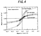
- Fig. 4 shows the magnetization hysteresis loops of the CrSb layers provided in Example 1-3. As is apparent from Fig. 4, all the CrSb layers exhibit ferromagnetic properties at room temperature. Therefore, all the CrSb layers can be utilized as zinc blende type CrSb compounds according to the present invention.
- the magnetization of the CrSb layer provided in Example 2 or 3 is larger than the one of the CrSb layer provided in Example 1 because the CrSb is formed on the GaSb underlayer or the AlGaSb underlayer, instead of the GaAs underlayer.
- the magnetization of the CrSb layer formed on the AlGaSb underlayer in Example 3 is larger than the one of the CrSb layer formed on the GaSb underlayer in Example 2.
- a zinc blende type CrSb compound to exhibit ferromagnetic properties at room temperature a method for fabricating the zinc blende type CrSb compound can be provided, according to the present invention. Also, a multilayered structure including the zinc blende type CrSb compound can be provided. Therefore, a composite device composed of semiconductor element and ferromagnetic element can be realized.
Landscapes
- Chemical & Material Sciences (AREA)
- Engineering & Computer Science (AREA)
- Crystallography & Structural Chemistry (AREA)
- Organic Chemistry (AREA)
- Materials Engineering (AREA)
- Metallurgy (AREA)
- Power Engineering (AREA)
- Nanotechnology (AREA)
- Inorganic Chemistry (AREA)
- Physical Deposition Of Substances That Are Components Of Semiconductor Devices (AREA)
Abstract
Description
- This invention relates to a zinc blende type CrSb compound, a method for fabricating a zinc blende type CrSb compound and a multilayered structure including a zinc blende type CrSb compound as a ferromagnetic layer.
- With the development of crystal growth technique such as molecular beam epitaxy (MBE method), a different kind of metallic element can be doped into a semiconductor. Particularly, a magnetic semiconductor which is made by doping a magnetic element into a semiconductor has been intensely researched and developed. If a ferromagnetic film is epitaxially grown on a semiconductor, a much higher performance composite device than a conventional one can be provided because conventional semiconductor electronics technique is combined with ferromagnetic properties.
- A CrSb compound has been expected as a ferromagnetic material to constitute a ferromagnetic layer of the composite device. With normal epitaxial growth technique, however, only CrSb compound of NiAs type crystal structure can be fabricated. Then, the CrSb compound exhibits anti-ferromagnetic properties at room temperature. Moreover, such an attempt is made as to fabricate a CrSb/Sb super lattice structure and thus, to create ferromagnetic properties in the structure, but, as of now, can not be realized at room temperature.
- It is an object of the present invention to provide CrSb to exhibit ferromagnetic properties at room temperature and a method for fabricating the CrSb.
- In order to achieve the above object, this invention relates to a zinc blende type CrSb compound.
- This invention also relates to a method for fabricating a zinc blende type CrSb compound, comprising the steps of:
- preparing a given substrate,
- forming an underlayer made of a III-V semiconductor compound on the substrate, and
- epitaxially growing a CrSb compound on the underlayer by means of MBE method to fabricate a zinc blende type CrSb compound.
-
- The inventors had been intensely studied to achieve the above object. As a result, they found out that the zinc blende type CrSb compound can be fabricated by forming an underlayer made of a III-V semiconductor compound on a given substrate and epitaxially growing a CrSb layer on the underlayer by means of a MBE method, according to the fabricating method of the present invention. In this case, the CrSb layer itself has the zinc blende type crystal structure. The zinc blende type CrSb compound has a much larger ferromagnetic transition temperature than room temperature, and then, can exhibit ferromagnetic properties at room temperature.
- That is, if a given CrSb layer is formed according to the present invention, a zinc blende type CrSb compound to exhibit ferromagnetic properties at room temperature can be provided, as mentioned above. Therefore, if a ferromagnetic layer of a given composite device is made of the zinc blende type CrSb compound, the composite device can exhibit extreme device performances.
- A multilayered structure according to the present invention can be obtained by performing the fabricating method of the present invention, and then, comprises a given substrate, an underlayer made of a III-V semiconductor compound and formed on the substrate, and a CrSb compound layer having a zinc blende type crystal structure and formed on the underlayer.
- In the multilayerd structure, the CrSb layer is formed as a ferromagnetic layer on the III-V semiconductor compound layer as an underlayer, so the multilayered structure has a stacking structure of semiconductor layer/ferromagnetic layer. Therefore, the multilayered structure may be preferably employed for the composite device.
- For better understanding of the present invention, reference is made to the attached drawings, wherein
- Fig. 1 is a structural view showing a multilayered structure including a zinc blende type CrSb layer according to the present invention,
- Fig. 2 is a structural view showing another multilayered structure including a zinc blende type CrSb layer according to the present invention,
- Fig. 3 is a structural view showing still another multilayered structure including a zinc blende type CrSb layer according to the present invention, and
- Fig. 4 is a graph showing a magnetic property of a zinc blende type CrSb compound according to the present invention.
-
- This invention will be described in detail with reference to the accompanying drawings. In the present invention, an underlayer made of a III-V semiconductor compound is formed on a given substrate, and then, a CrSb layer is epitaxially grown on the underlayer by means of a MBE method. The CrSb layer results in having zinc blende crystal structure.
- The thickness of the underlayer is not restricted only if the zinc blende type CrSb compound can be fabricated by means of a MBE method. However, the thickness of the underlayer is preferably set within 2-1000 nm, particularly within 40-400 nm.
- The underlayer may be made of a binary, ternary or quaternary III-V semiconductor compound. Particularly, the underlayer is preferably made of a semiconductor compound having a composition of AlXGa1-XAs (0≤X≤1) or AlXGa1-XSb (0≤X≤1). In this case, the zinc blende type CrSb compound can exhibit large magnetization at room temperature, and thus, good ferromagnetic performances at room temperature. The underlayer may be made by means of a conventional film-forming method such as a MBE method.
- In forming the CrSb layer on the underlayer made of a III-V semiconductor compound, the epitaxial growth temperature is preferably set within 200-600°C, particularly within 250-450°C.
- Also, the epitaxial growth rate is preferably set within 3-50nm/minute, particularly within 8-20nm/minute.
- With the above-mentioned fabricating process, the CrSb layer can exhibit ferromagnetic properties at room temperature because the ferromagnetic transition temperature is 400K or over. The thickness of the CrSb layer is preferably set within 0.3-300nm. The CrSb layer has zinc blende crystal structure, so the zinc blende type CrSb compound can be obtained from the CrSb layer, and thus, has a layered shape.
- It is desired that a buffer layer made of a III-V semiconductor compound is formed between the substrate and the underlayer. In This case, the lattice strain caused by the difference in lattice constant between the substrate and the underlayer can be relaxed effectively.
As a result, the ferromagnetic properties of the CrSb layer and thus, the zinc blende type CrSb compound can be developed. - Concretely, in the case of making the underlayer of a semiconductor compound having a composition of AlXGa1-XAs (0≤X≤1), the buffer layer is preferably made of a similar composition material of AlYGa1-YAs (0≤Y≤1). In the case of making the underlayer of AlXGa1-XSb (0≤X≤1), the buffer layer is preferably made of a similar composition material of AlYGa1-YSb (0≤Y≤1).
- More concretely, in the case of making the underlayer of AlXGa1-XAs (0≤X≤1), the buffer layer is preferably made of GaAs. In the case of making the underlayer of AlXGa1-XSb (0≤X≤1), the buffer layer is preferably made of AlSb. The thickness of the buffer layer is appropriately set on the kind of the substrate, the material kind and the thickness of the underlayer.
- The buffer layer may be constructed as a multilayered structure which is composed of two or over III-V semiconductor layers. In this case, the lattice strain caused by the difference in lattice constant between the substrate and the underlayer can be relaxed effectively, so that the crystallinity of the CrSb layer and thus, the zinc blende type CrSb can be more enhanced. As a result, the magnetic properties of the zinc blende type CrSb compound can be more enhanced.
- The buffer layer may be formed by means of a conventional film-forming method such as a MBE method.
- The kind of the substrate to be employed is not restricted, but in view of the epitaxial growth of the underlayer and the buffer layer which are made of III-V semiconductor compounds, the substrate is preferably made of a IIIV- semiconductor compound.
- The present invention will be described concretely, with reference to Examples.
- In this Example, a multilayered structure including a zinc blende type CrSb compound shown in Fig. 1 was fabricated. A (001) GaAs substrate was employed and set in a MBE apparatus. Then, the GaAs substrate was heated to 580°C, and an oxide film was desorbed from the GaAs substrate surface. Then, the GaAs substrate was heated to 560°C, and Ga beams and Sb beams were irradiated simultaneously onto the GaAs substrate, to form a GaAs layer as an underlayer in a thickness of 500nm on the GaAs substrate.
- Then, the GaAs substrate was cooled down while the Sb beams were irradiated. The irradiation of the Sb beams was stopped when the GaAs substrate was cooled down to 400°C. Then, Cr beams and Sb beams were irradiated simultaneously onto the GaAs underlayer, to form a CrSb layer in a thickness of 0.6nm on the GaAs underlayer while the GaAs substrate was held at 250°C.
- In this case, the forming rate of the CrSb layer was set to 6nm/sec. When the crystallinity of the CrSb layer was investigated by means of reflection high-energy electron diffraction (RHEED), it was turned out that the CrSb layer has zinc blende type RHEED pattern.
- In this Example, a multilayered structure including a zinc blende type CrSb compound shown in Fig. 2 was fabricated. A (001) GaAs substrate was employed and set in a MBE apparatus, as mentioned in Example 1. Then, an oxide film was desorbed from the GaAs substrate surface in the same manner. Then, the GaAs substrate was heated to 530°C, and a GaAs buffer layer was formed in a thickness of 100nm on the GaAs substrate by means of a MBE method. Then, Ga beams and Sb beams were irradiated simultaneously onto the GaAs buffer layer, to form a GaSb underlayer in a thickness of 400nm on the GaAs buffer layer.
- Then, a CrSb layer was formed in a thickness of 0.6nm on the GaSb underlayer in the same manner as in Example 1. When the crystallinity of the CrSb layer was investigated by means of reflection high-energy electron diffraction (RHEED), it was turned out that the CrSb layer has zinc blende type RHEED pattern.
- In this Example, a multilayered structure including a zinc blende type CrSb compound shown in Fig. 3 was fabricated. A (001) GaAs substrate was employed and set in a MBE apparatus, as mentioned in Example 1. Then, an oxide film was desorbed from the GaAs substrate surface in the same manner. Then, the GaAs substrate was heated to 530°C, and a GaAs buffer layer was formed in a thickness of 100nm on the GaAs substrate by means of a MBE method. Then, Al beams, Ga beams and Sb beams were irradiated simultaneously onto the GaAs buffer layer, to form an AlGaSb underlayer in a thickness of 400nm on the GaAs buffer layer.
- Then, a CrSb layer was formed in a thickness of 0.3nm on the AlGaSb underlayer in the same manner as in Example 1. When the crystallinity of the CrSb layer was investigated by means of reflection high-energy electron diffraction (RHEED), it was turned out that the CrSb layer has zinc blende type RHEED pattern.
- Fig. 4 shows the magnetization hysteresis loops of the CrSb layers provided in Example 1-3. As is apparent from Fig. 4, all the CrSb layers exhibit ferromagnetic properties at room temperature.
Therefore, all the CrSb layers can be utilized as zinc blende type CrSb compounds according to the present invention. - Also, the magnetization of the CrSb layer provided in Example 2 or 3 is larger than the one of the CrSb layer provided in Example 1 because the CrSb is formed on the GaSb underlayer or the AlGaSb underlayer, instead of the GaAs underlayer. Moreover, the magnetization of the CrSb layer formed on the AlGaSb underlayer in Example 3 is larger than the one of the CrSb layer formed on the GaSb underlayer in Example 2.
- Although the present invention was described in detail with reference to the above examples, this invention is not limited to the above disclosure and every kind of variation and modification may be made without departing from the scope of the present invention. For example, in the above embodiments, only one underlayer and only one CrSb layer are prepared, but plural underlayers and plural CrSb layers may be prepared and alternately stacked on the GaAs substrate.
- As mentioned above, a zinc blende type CrSb compound to exhibit ferromagnetic properties at room temperature, a method for fabricating the zinc blende type CrSb compound can be provided, according to the present invention. Also, a multilayered structure including the zinc blende type CrSb compound can be provided. Therefore, a composite device composed of semiconductor element and ferromagnetic element can be realized.
Claims (18)
- A zinc blende type CrSb compound.
- A zinc blende type CrSb compound as defined in claim 1, having a layered shape and having a thickness within 0.3-300nm.
- A zinc blende type CrSb compound as defined in claim 1 or 2, having a ferromagnetic transition temperature of 400K or over.
- A method for fabricating a zinc blende type CrSb compound, comprising the steps of:preparing a given substrate,forming an underlayer made of a III-V semiconductor compound on said substrate, andepitaxially growing a CrSb compound on said underlayer by means of MBE method to fabricate a zinc blende type CrSb compound.
- A fabricating method as defined in claim 4, wherein the thickness of said underlayer is set within 2-1000nm.
- A fabricating method as defined in claim 4 or 5, wherein said underlayer is made of AlXGa1-XAs (0≤X≤1)
- A fabricating method as defined in claim 4 or 5, wherein said underlayer is made of AlXGa1-XSb (0≤X≤1).
- A fabricating method as defined in any one of claims 4-7, wherein the epitaxial growth temperature of said CrSb compound is set within 250-400°C.
- A fabricating method as defined in any one of claims 4-8, wherein the epitaxial growth rate of said CrSb compound is set within 3-50nm/minute.
- A fabricating method as defined in any one of claims 4-9, further comprising the step of forming a buffer layer made of a III-V semiconductor compound between said substrate and said underlayer.
- A fabricating method as defined in claim 10, wherein said buffer layer is composed of a multilayered structure made of two or over III-V semiconductor layers.
- A multilayered structure comprising a given substrate, an underlayer made of a III-V semiconductor compound and formed on said substrate, and a CrSb compound layer having a zinc blende type crystal structure and formed on said underlayer.
- A multilayered structure comprising a given substrate, plural underlayers made of III-V semiconductor compounds, and plural CrSb compound layers having zinc blende type crystal structures, wherein said underlayers and said CrSb compound layers are alternately stacked on said substrate.
- A multilayered structure as defined in claim 12 or 13, wherein the thickness of said underlayer is set within 2-1000nm.
- A multilayered structure as defined in any one of claims 12-14, wherein said underlayer is made of AlXGa1-XAs (0≤X≤1).
- A multilayered structure as defined in any one of claims 12-14, wherein said underlayer is made of AlXGa1-XSb (0≤X≤1).
- A multilayered structure as defined in any one of claims 12-16, further comprising a buffer layer made of a III-V semiconductor compound between said substrate and said underlayer.
- A multilayered structure as defined in claim 17, wherein said buffer layer is composed of a multilayered structure made of two or over III-V semiconductor layers.
Applications Claiming Priority (2)
| Application Number | Priority Date | Filing Date | Title |
|---|---|---|---|
| JP2001189191 | 2001-06-22 | ||
| JP2001189191 | 2001-06-22 |
Publications (2)
| Publication Number | Publication Date |
|---|---|
| EP1271569A2 true EP1271569A2 (en) | 2003-01-02 |
| EP1271569A3 EP1271569A3 (en) | 2003-01-22 |
Family
ID=19028151
Family Applications (1)
| Application Number | Title | Priority Date | Filing Date |
|---|---|---|---|
| EP02013829A Withdrawn EP1271569A3 (en) | 2001-06-22 | 2002-06-21 | Zinc blende type CrSb compound, method for fabricating the same, and multilayered structure |
Country Status (3)
| Country | Link |
|---|---|
| US (1) | US6861342B2 (en) |
| EP (1) | EP1271569A3 (en) |
| KR (1) | KR20030001290A (en) |
Families Citing this family (5)
| Publication number | Priority date | Publication date | Assignee | Title |
|---|---|---|---|---|
| KR100499180B1 (en) * | 2002-12-14 | 2005-07-01 | 강태원 | Method of manufacturing Ferromagnetic semiconductor having quantum dots |
| CN100355017C (en) * | 2005-05-16 | 2007-12-12 | 中国科学院半导体研究所 | Growth process capable of increasing zb-CrSb thickness |
| US8886125B2 (en) * | 2006-04-14 | 2014-11-11 | Qualcomm Incorporated | Distance-based association |
| CN112160026A (en) * | 2020-08-25 | 2021-01-01 | 江苏大学 | Chromium telluride thin film embedded into multiple nano-sheets, and preparation method and application thereof |
| CN119352146B (en) * | 2024-12-26 | 2025-04-11 | 大连理工大学 | Preparation method and application of high-quality single-cell thickness chromium-antimony magnetic film |
Family Cites Families (3)
| Publication number | Priority date | Publication date | Assignee | Title |
|---|---|---|---|---|
| US5464990A (en) * | 1992-09-25 | 1995-11-07 | Fuji Xerox Co., Ltd. | Voltage non-linear device and liquid crystal display device incorporating same |
| US5563019A (en) * | 1994-06-30 | 1996-10-08 | E. I. Du Pont De Nemours And Company | Donor element for laser-induced thermal transfer |
| US6294308B1 (en) * | 1999-10-15 | 2001-09-25 | E. I. Du Pont De Nemours And Company | Thermal imaging process and products using image rigidification |
-
2002
- 2002-06-18 US US10/172,999 patent/US6861342B2/en not_active Expired - Fee Related
- 2002-06-21 KR KR1020020034849A patent/KR20030001290A/en not_active Ceased
- 2002-06-21 EP EP02013829A patent/EP1271569A3/en not_active Withdrawn
Non-Patent Citations (4)
| Title |
|---|
| DOHNOMAE H ET AL: "Structural and magnetic properties of Cr/Sb multilayers" ACSI-1. FIRST INTERNATIONAL SYMPOSIUM ON ATOMICALLY CONTROLLED SURFACES AND INTERFACES, TOKYO, JAPAN, 19-22 NOV. 1991, vol. 60-61, pages 807-812, XP002219850 Applied Surface Science, Aug. 1992, Netherlands ISSN: 0169-4332 * |
| DOHNOMAE H: "X-ray diffraction and electron microscopy study of Cr/Sb multilayered films" JAPANESE JOURNAL OF APPLIED PHYSICS, PART 1 (REGULAR PAPERS & SHORT NOTES), MARCH 1994, JAPAN, vol. 33, no. 3A, pages 1499-1508, XP001107208 ISSN: 0021-4922 * |
| RADHAKRISHNA P ET AL: "Inelastic-neutron-scattering studies of spin-wave excitations in the pnictides MnSb and CrSb" PHYSICAL REVIEW B (CONDENSED MATTER), 1 NOV. 1996, APS THROUGH AIP, USA, vol. 54, no. 17, pages 11940-11943, XP002219849 ISSN: 0163-1829 * |
| ZHAO J H ET AL: "Room-temperature ferromagnetism in zincblende CrSb grown by molecular-beam epitaxy" APPLIED PHYSICS LETTERS, 22 OCT. 2001, AIP, USA, vol. 79, no. 17, pages 2776-2778, XP001107207 ISSN: 0003-6951 * |
Also Published As
| Publication number | Publication date |
|---|---|
| US20030003704A1 (en) | 2003-01-02 |
| KR20030001290A (en) | 2003-01-06 |
| US6861342B2 (en) | 2005-03-01 |
| EP1271569A3 (en) | 2003-01-22 |
Similar Documents
| Publication | Publication Date | Title |
|---|---|---|
| US6583436B2 (en) | Strain-engineered, self-assembled, semiconductor quantum dot lattices | |
| US20010023942A1 (en) | Semiconductor device of heterojunction structure having quantum dot buffer layer | |
| CA1098624A (en) | Type of superlattice | |
| JP7109062B2 (en) | Quantum dot sheet, optoelectronic device using the same, and method for producing quantum dot sheet | |
| US6861342B2 (en) | Zinc blende type CrSb compound, method for fabricating the same, and multilayered structure | |
| US20020031900A1 (en) | Method for aligning quantum dots and semiconductor device fabricated by using the same | |
| JP2013093425A (en) | Quantum semiconductor device and method for manufacturing the same | |
| JP3849015B2 (en) | Method for producing zinc blende type CrSb and multilayer film structure | |
| JPH0722312A (en) | Method for manufacturing strained semiconductor film | |
| JP3692407B2 (en) | Manufacturing method of semiconductor quantum dot device | |
| JP3146457B2 (en) | Method for manufacturing quantum wire structure | |
| JP3250495B2 (en) | Semiconductor structure and semiconductor crystal growth method | |
| JP3169064B2 (en) | Fabrication method of semiconductor three-dimensional quantum structure | |
| JP2970103B2 (en) | Semiconductor superlattice structure | |
| US20250212698A1 (en) | Semiconductor-superconductor hybrid structure | |
| JP2790006B2 (en) | Hetero interface formation method | |
| JP3224118B2 (en) | Epitaxial growth method | |
| Díaz et al. | Vertically ordered magnetic EuTe quantum dots stacks on SnTe matrices | |
| JP2672581B2 (en) | Semiconductor device | |
| JP2847307B2 (en) | Magnetic semiconductor device, method of manufacturing the same, and magneto-optical read head | |
| JPS5973499A (en) | Growth of compound semiconductor | |
| JP2875295B2 (en) | Manganese aluminum superlattice magnetic film | |
| CN111446313A (en) | Quantum well structure and growth method thereof | |
| JPH0410527A (en) | Semiconductor superlattice | |
| JPH04282826A (en) | Quantum fine wire structure body and manufacture thereof |
Legal Events
| Date | Code | Title | Description |
|---|---|---|---|
| PUAI | Public reference made under article 153(3) epc to a published international application that has entered the european phase |
Free format text: ORIGINAL CODE: 0009012 |
|
| PUAL | Search report despatched |
Free format text: ORIGINAL CODE: 0009013 |
|
| 17P | Request for examination filed |
Effective date: 20020621 |
|
| AK | Designated contracting states |
Kind code of ref document: A2 Designated state(s): AT BE CH CY DE DK ES FI FR GB GR IE IT LI LU MC NL PT SE TR |
|
| AX | Request for extension of the european patent |
Free format text: AL;LT;LV;MK;RO;SI |
|
| AK | Designated contracting states |
Kind code of ref document: A3 Designated state(s): AT BE CH CY DE DK ES FI FR GB GR IE IT LI LU MC NL PT SE TR |
|
| AX | Request for extension of the european patent |
Free format text: AL;LT;LV;MK;RO;SI |
|
| AKX | Designation fees paid |
Designated state(s): DE FR GB |
|
| STAA | Information on the status of an ep patent application or granted ep patent |
Free format text: STATUS: THE APPLICATION HAS BEEN WITHDRAWN |
|
| 18W | Application withdrawn |
Effective date: 20050408 |