EP1271543A2 - Method and system for fast memory access - Google Patents
Method and system for fast memory access Download PDFInfo
- Publication number
- EP1271543A2 EP1271543A2 EP02254515A EP02254515A EP1271543A2 EP 1271543 A2 EP1271543 A2 EP 1271543A2 EP 02254515 A EP02254515 A EP 02254515A EP 02254515 A EP02254515 A EP 02254515A EP 1271543 A2 EP1271543 A2 EP 1271543A2
- Authority
- EP
- European Patent Office
- Prior art keywords
- memory
- address
- memory section
- data word
- data
- Prior art date
- Legal status (The legal status is an assumption and is not a legal conclusion. Google has not performed a legal analysis and makes no representation as to the accuracy of the status listed.)
- Withdrawn
Links
- 230000015654 memory Effects 0.000 title claims abstract description 240
- 238000000034 method Methods 0.000 title claims description 34
- 239000000872 buffer Substances 0.000 claims abstract description 38
- 230000003139 buffering effect Effects 0.000 claims 1
- 240000007320 Pinus strobus Species 0.000 description 11
- 238000010586 diagram Methods 0.000 description 5
- 238000013459 approach Methods 0.000 description 2
- 238000003491 array Methods 0.000 description 1
- 238000005516 engineering process Methods 0.000 description 1
- 230000006870 function Effects 0.000 description 1
- 238000012986 modification Methods 0.000 description 1
- 230000004048 modification Effects 0.000 description 1
- 230000002093 peripheral effect Effects 0.000 description 1
- 229920000747 poly(lactic acid) Polymers 0.000 description 1
Images




Classifications
-
- G—PHYSICS
- G11—INFORMATION STORAGE
- G11C—STATIC STORES
- G11C7/00—Arrangements for writing information into, or reading information out from, a digital store
- G11C7/10—Input/output [I/O] data interface arrangements, e.g. I/O data control circuits, I/O data buffers
- G11C7/1006—Data managing, e.g. manipulating data before writing or reading out, data bus switches or control circuits therefor
Definitions
- This invention relates to methods and systems for fast access of computer-based memories.
- Modern computer-based systems often use wide memories that have a constant width. However, these systems must often manipulate a variety of variables having different data widths. For instance, a particular processor can have a thirty-two bit (four byte) wide bus with a thirty-two bit wide random access memory (RAM), but must manipulate any number of variables having eight bit (one byte), sixteen bit (two bytes) or thirty-two bit widths.
- a particular processor can have a thirty-two bit (four byte) wide bus with a thirty-two bit wide random access memory (RAM), but must manipulate any number of variables having eight bit (one byte), sixteen bit (two bytes) or thirty-two bit widths.
- RAM random access memory
- a first variable in a block of thirty-two bit wide RAM may be a byte-wide variable while a second variable may be a four-byte variable.
- the first variable will occupy the first byte of a first memory location, while the second variable will occupy the remaining three bytes of the first memory location plus the first byte of the next memory location.
- a computer accessing the second variable can take two separate memory-access cycles to either read or write the second variable.
- Preferred embodiments of the invention provide techniques to access a misaligned data word in a single memory-access cycle.
- the techniques use a first memory section connected to a first address bus, a second memory section connected to a second address bus and an address device that simultaneously provides a first address to the first memory section using the first address bus and a second, incrementally higher, address to the second memory section using the second address bus.
- the first and second memory sections are preferably separate memory arrays.
- buffer circuitry can receive a first portion of the misaligned data word from the first memory section and receive a second portion of the misaligned data word from the second memory section and assemble the data in the data word from the first and second portions.
- the buffer circuitry can effectively perform a shift operation on the data in the data word, then write a first portion of the shifted word to the first memory section and write a second portion of the shifted word to the second memory section.
- a frequent problem that arises with modern computer-based systems is that, while the widths of an available physical memory are fixed, the widths of various data types can vary. For example, a particular microcomputer may have a sixty-four bit wide memory, but may be required to access and manipulate eight-bit, sixteen-bit, thirty-two bit and sixty-four bit data.
- One problem that can arise with such systems is that different data variables can become misaligned with the address boundaries of the physical memories.
- the first variable in a block of sixty-four bit wide memory may be a single byte-wide variable, while the second variable may be an eight byte-wide variable.
- the first variable will occupy a first byte of the first memory location
- the second variable will occupy the remaining seven bytes of the first memory location plus the first byte of the next memory location.
- misaligned data can be accessed in a single memory-access cycle.
- the eight-byte misaligned data variable can be written in a single memory-access cycle by splitting the eight-byte variable into a first portion having the first seven bytes and a second portion having the last byte. Assuming that separate addresses and control signals are provided for each of the two physical memories, the first portion of the data variable can then be written to the last seven bytes of the first memory while the second portion can be simultaneously written to the first byte of the second memory.
- data can be read by providing consecutive addresses to the first and second memories, selectively reading the desired bytes and then appropriately combining the selected bytes.
- Figure 1 is a block diagram of a system 100 capable of accessing misaligned data in a single cycle.
- the system 100 includes a first data buffer block 110, and address device 130, a second data buffer block 140, an even memory section 120-A and an odd memory section 120-B.
- misaligned data can be written to the memory sections 120-A and 120-B in a single memory-access cycle.
- the exemplary memory sections 120-A and 120-B are each sixty-four bit wide (eight byte) devices each having 262,144 (2 18 ) separate locations. However, rather than appear as single memory having a width of 128 bits by 262,144 locations, the memory sections 120-A and 120-B can appear as a single physical memory having a width of sixty-four bits and 524,288 interleaved memory locations.
- the first four memory locations of memory section 120-A can appear as addressed locations zero, two, four, six and eight, while the first four memory locations of memory section 120-B can appear as addressed locations one, three, five, seven and nine.
- an external device writing to the memory sections 120-A and 120-B can provide a data word to the first data buffer block 110 via link 102, and further provide address and control signals to the address device 130 via links 104 and 106 respectively.
- the address device 130 can make a determination whether a particular variable is misaligned, i.e., whether a particular data variable crosses the sixty-four bit physical memory boundary.
- the address device 130 can provide an offset to the first data buffer 110 via link 138-W. For example, if a particular eight-byte data variable is misaligned such that the first byte of the misaligned data variable is located at the sixth byte of the physical memory, the address device 130 can provide an offset of five to the first data buffer block 110.
- the address device 130 can further provide address and control information to the memory sections 120-A and 120-B.
- the appropriate addressing information is provided to the memory sections 120-A and 120-B via links 132-A and 132-B, respectively.
- the write control information is provided to the memory sections 120-A and 120-B via links 134-A and 134-B, respectively.
- the address device 130 can provide a first address to memory section 120-A and a second address to memory location 120-B, where the second address is incrementally larger than the first address.
- the address device 130 can provide write control information that can cause a write operation for the upper three bytes of the first memory section 120-A and the lower five bytes of the second memory section 120-B.
- the first data buffer block 110 can receive the data variable along with the offset information, manipulate and divide the data into a first portion and second portion and appropriately feed the first portion to one memory section 120-A or 120-B and the second portion to the other memory section 120-B or 120-A.
- a link 112-A conveys data from the first data buffer 110 to the first memory section 120-A and another link 112-B conveys data from the first buffer 110 to the second memory section 120-B.
- the first data buffer block 110 can direct the low three bytes of the data variable to the high three bytes of memory section 120-A, and further provide the high five bytes of the data variable to the low five bytes of memory section 120-B.
- the memory sections 120-A and 120-B can receive their respective data portions along with the address and control information and appropriately store the data. That is, memory section 120-A can store the low three bytes of the data variable in the high three bytes of a memory location having a first address, while memory section 120-B can store the high five bytes of the data variable in the low five bytes of a memory location having a second address, where the second address will be one location higher than the first address. Accordingly, as data is provided to the various memory sections 120-A and 120-B, the address and control information can simultaneously accommodate a misaligned write operation to both memory locations in a single cycle.
- the system 100 can read a misaligned data variable from the memory sections 120-A and 120-B.
- the address device 130 can receive the address and control signals, provide an offset to the second data buffer block 140 via link 138-R, provide the appropriate addressing information to memory sections 120-A and 120-B via links 132-A and 132-B respectively and further provide the appropriate read control information to memory sections 120-A and 120-B via links 136-A and 136-B respectively.
- the memory sections 120-A and 120-B can receive the address and read control information and provide the appropriate bytes of data to the second data buffer 140 via links 122-A and 122-B.
- the second data buffer block 140 in turn can receive the data bytes from the memory sections 120-A and 120-B and combine the received data bytes into a single data variable taking into account the offset provided by the address device 130.
- the second data buffer block 140 can receive the various bytes, combine the various bytes into a single contiguous data variable having eight bytes, appropriately shift the combined data variable by six bytes and provide the combined/shifted data variable to an external device.
- the exemplary first data buffer block 110 can be a portion of integrated circuit containing various logic circuits that can receive a data variable of a given size, effectively perform a circular-barrel shift/multiplexing operation on the received data variable and provide portions of the shifted/multiplexed data variable to the memory sections 120-A and 120-B.
- the first data buffer block can use any combination of elements, such as shifters, barrel shifters, multiplexers, various sum-of-products-based logic, or any other known or later developed combination of systems and devices that can receive a data variable, perform the equivalent of a shifting operation on the received data variable and provide the shifted data to the memory sections 120-A and 120-B without departing from the scope of the present invention as defined in the claims.
- elements such as shifters, barrel shifters, multiplexers, various sum-of-products-based logic, or any other known or later developed combination of systems and devices that can receive a data variable, perform the equivalent of a shifting operation on the received data variable and provide the shifted data to the memory sections 120-A and 120-B without departing from the scope of the present invention as defined in the claims.
- the second data buffer block 140 can be a portion of an integrated circuit containing various logic circuits.
- the second data buffer block 140 can be any device capable of receiving various portions of data from multiple memories, combine the received data portions, and provide the combined data to an external device without departing from the scope of the present invention as defined in the claims.
- the address device 130 can be a collection of logic circuits on a portion of an integrated circuit.
- the address device 130 can be any combination of systems and devices capable of receiving address and control signals from an external device and providing address and control information to memory sections 120-A and 120-B as well as offset information to the data buffers 110 and 130 without departing from the spirit of the present invention as defined in the claims.
- Figure 2 depicts a memory system, such as the memory sections 120-A and 120-B of Figure 1.
- the memory system 120 includes a number of byte-wide memory modules 120-1, 120-2...120-k.
- the various memory modules 120-1, 120-2, ...120-k each have a data input port 112-1, 112-2, ...112-k, a data output port 122-1, 122-2, ...122-k, an address port 132-1, 132-2, ...132-k, a write port 134-1, 134-2, ...134-k and a read port 136-1, 136-2, ...136-k.
- a data can be selectively written to any combination of the memory modules 120-1, 120-2, ...120-k by providing the appropriate data to each of the data input ports 112-1, 112-2, ...112-k via bus 112 while applying the appropriate address information to the address ports 132-1, 132-2, ...132-k via bus 132 and write control information, such as write strobes, to the appropriate write ports 134-1, 134-2, ...134-k via bus 134.
- write control information such as write strobes
- data can be read from the memory system 120, by providing the appropriate address information to the various address ports 132-1, 132-2, ...132-k via bus 132 as well as the appropriate read control information, such as read strobes, to the various read ports 136-1, 136-2, ...136-k via bus 136.
- the appropriate memory modules 120-1, 120-2, ...120-k will enable output buffers associated with their output ports 122-1, 122-2, ...122-k such that data stored within each module 120-1, 120-2, ...120-k can be provided to data-bus 122.
- the array of individual read strobes can be replace by a single read strobe with the understanding that using a single read strobe may cause the memory system 120 to use more power.
- exemplary memory modules 120-1, 120-2, ...120-k are controlled using read and write strobes
- the various memory modules 120-1, 120-2, ...120-k can be controlled using a variety of signals including read strobes, write strobes, chip selects, output enable signals, or any other signal useful for selectively writing data to, or reading data from, a memory device without departing from the scope of the present invention as defined in the claims.
- the exemplary memory modules 120-1, 120-2, ...120-k are high-speed random access memory (RAM) integrated circuits with each device being eight bits wide and having 242,144 separate locations.
- RAM random access memory
- the various memory modules 120-1, 120-2, ...120-k can be any other known memory device capable of being selectively read or written to, such as RAMs, read only memories (ROMs), EPROMs, EEPROMs, and the like.
- ROMs read only memories
- EPROMs EPROMs
- EEPROMs electrically erasable programmable read only memory
- the particular width and depth of each memory module, 120-1, 120-2, ...120-k can vary as desired or otherwise required by design, without departing from the scope of the present invention as defined in the claims.
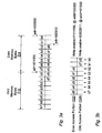
- Figures 3A and 3B depict the operations of a misaligned data word being written to a system, such as a memory system depicted in figures 1 and 2.
- a data variable ⁇ d7...d0 ⁇ can be misaligned with respect to a physical memory consisting of eight bytes ⁇ b7...b0 ⁇ .
- the logical width of a physical memory may appear as eight bytes ⁇ b7...b0 ⁇ , as discussed above the actual physical data width can be sixteen bytes ⁇ b7...b0, b7...b0 ⁇ of data including a number of odd memory bytes 312 and even memory bytes 314.
- the exemplary data variable is offset by two bytes
- the low six bytes of the data variable ⁇ d5...d0 ⁇ can be written to the high bytes ⁇ b7...b2 ⁇ respectively of the even memory bytes 314.
- high two data variable bytes ⁇ d7, d6 ⁇ can be written to the two low memory bytes ⁇ b1, b0 ⁇ respectively of the odd memory bytes 312.
- Figure 3B depicts the data variable ⁇ d7...d0 ⁇ shown in Figure 3A broken into an even portion 322 consisting of data variable bytes ⁇ d5...d0 ⁇ and an odd portion 334 consisting of data variable bytes ⁇ d7, d6 ⁇ .
- write enable signals "11111100” representing an array of write strobes can be provided to an array of individual byte-wide memory modules of an even memory (at a relative address of "00000”) to activate write operations at the appropriate memory modules.
- a write enable signals of "00000011” can be similarly applied to another array of memory modules at a relative address of "01000” to activate write operations at the appropriate odd memory modules.
- Figures 4A-4C depict a second memory access operation where a four-byte data variable ⁇ d3...d0 ⁇ can be read from a memory system capable of reading a misaligned data variable in a single cycle.
- the data variable ⁇ d3...d0 ⁇ has an offset of five bytes such that data variable bytes ⁇ d2, d1, d0 ⁇ can be read from the high three memory bytes ⁇ b7, b6, b5 ⁇ of even memory bytes 414 and data variable byte ⁇ d3 ⁇ can be read from the low memory byte ⁇ b0 ⁇ of odd memory bytes 412.
- Figure 4B depicts the data variable ⁇ d3...d0 ⁇ of Figure 4A broken into an even portion 422 and an odd portion 424 with data variable bytes ⁇ d2, d1, d0 ⁇ included in the even portion 422 and data variable byte ⁇ d3 ⁇ included in the odd portion 424. Since only the upper three bytes ⁇ b7, b6, b5 ⁇ of the even portion 422 are to be read, read enable signals of "11100000" can be applied to respective byte-wide memory modules of an even portion memory. Similarly, because only data byte ⁇ b0 ⁇ is to be read from the odd portion 424, read enable signals of "00000001" can be applied to an array of memory modules that comprise an odd memory.
- Figure 4C demonstrates that the bytes of the data variable ⁇ d3..d0 ⁇ can be combined and shifted such that the various bytes ⁇ d3..d0 ⁇ of the data variable are respectively aligned with memory bytes ⁇ b3..b0 ⁇ .
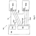
- Figure 5 is a second exemplary embodiment of a system 500 capable of reading and writing misaligned data variables in a single memory-access cycle.
- the system 500 includes a controller 502, an even memory section 520-A and an odd memory section 520-B.
- the controller 502 includes a data buffer block 510 and an address device 530.
- the second memory system 500 can read and write misaligned data bytes.
- the second memory system 500 can read and write data using a bi-directional bussed system.
- the data buffer block 510 can generate or otherwise derive data from controller 502, optionally shift the data, and provide the data to the even and odd memory sections 520-A and 520-B.
- the address device 530 can provide even address information and even write control information to the even memory section 520-A via links 114-A and 118-A respectively, and further provide odd address information and odd write control information to the odd memory section 520-B via links 114-B and 118-B respectively.
- the address device 530 can provide different address information to the different memory sections 520-A and 520-B, as well as a different write control information, such as an array of write strobes. Accordingly, by using the above-described technique, a data variable can be written to the memory sections 520-A and 520-B in a single memory-access cycle regardless of how the data variable is aligned.
- the controller 502 can read a data variable from the memory sections 520-A and 520-B in a single cycle regardless of the alignment of the data variable.
- the address device 530 can provide the appropriate addresses information as well as the appropriate read control information, such as an array of read strobes, to each of the even and odd memory sections 520-A and 520-B.
- the data buffer block 510 can receive the appropriate data bytes, then combine and shift the data bytes as is required by a particular operation of the controller 502.
- the address device 530 can provide address information using address busses that are partially disjoint. For example, assuming the address device 530 is a sixteen-bit address device, the address device 530 can provide the most significant eight address bits to both the even and odd memory sections 520-A and 520-B using eight shared address lines ⁇ A15...A8 ⁇ , while providing two separate sets of least significant address bits ⁇ A7...A0 ⁇ even and ⁇ A7...A0 ⁇ odd to memory sections 520-A and 520-B respectively.
- While providing partially disjoint address busses does not allow the system 500 to access every possible misaligned memory location in a single memory-access cycle, the total number of address lines is otherwise reduced. For the example above, assuming the address bus is sixteen bits wide with the upper most eight bits being shared, a single memory-access cycle access can be performed for 255 out of every 256 memory locations. However, the controller 502 requires eight fewer address ports/pins and supporting electronic circuits.
- the exemplary controller 502 can be a microcontroller-type device on an integrated circuit. However, it should be appreciated that the controller 502 can be any of various sequential instruction machines, such as a controller, a microcontroller, microprocessor, a processor, a digital signal processor or any other known or later developed device that can act as a sequential instruction machine and access various memories.
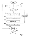
- FIG. 6 is a block diagram of a flowchart of a first exemplary operation.
- the process starts at step 600 where a data variable type is determined, i.e., the size of the data variable, as well as the address that the data variable is to be read from.
- step 610 a determination is made as to whether the data variable is aligned. That is, it is determined whether the data of the data variable exists in two separate logical memory locations. If the data variable is aligned, control jumps to steps 680; otherwise, control continues to step 620.
- step 680 data is read from a memory and control continues to step 650.
- step 620 even and odd address information, as well as even and odd read control information, is provided to each of two memory sections, such as the even and odd memory sections shown in figures 1 and 5.
- step 630 even and odd portions of the data variable are read from the even and odd memory sections.
- step 640 the even and odd portions are assembled into a single data variable.
- assembling a data variable can include logically combining the even and odd portions as well as shifting the combined portions such that the shifted data portions can be provided to an external device as a single data variable aligned with the least significant bytes of a logical bus. Control continues to step 650.
- step 650 the assembled data of 640 is provided to another device, such as an integrated sequential instruction machine.
- step 660 a determination is made as to whether to continue reading data variables. If further data variables are to be read, control jumps back to step 600; otherwise, control continues to step 670 where the process stops.
- Figure 7 is a flowchart outlining a second exemplary operation. As shown in Figure 7, the process starts at step 700 where the type and address of a particular data variable is determined. Next, at step 710, a determination is made as to whether the data variable is aligned. If the data variable is aligned, control jumps to step 800; otherwise, control continues to step 720. In step 800, data is written to a memory and control continues to step 760.
- step 720 even and odd address information, as well as even and odd write control information, is provided to even and odd memory sections.
- step 730 the data in the data variable is appropriately adjusted/manipulated by any of several operations that effectively perform a shifting operation such that the data can be provided to the appropriate memory modules of both an even and odd memory section.
- step 740 the data of the data variable is divided into an even portion and an odd portion with the even portion provided to an even memory section and the odd portion provided to an odd memory section. Control continues to step 750.
- step 750 the even and odd portions are effectively written to the even and odd memory sections.
- step 760 a determination is made as to whether the data written in steps 700-750 is to be read. If data is to be read, control jumps to step 810; otherwise, control continues to step 770.
- step 810 the appropriate data is read.
- the data read can be performed according to any number of techniques, such as the technique outlined in the flowchart of figure 6 or described according to figures 1-5. Control continues to step 770.
- step 770 a determination is made as to whether to continue to write and optionally read various data variables. If the operation is to continue, control jumps back to step 700; otherwise, control continues to step 780 where the process stops.
- the systems and methods embodying this invention are preferably implemented using dedicated logic or other integrated circuits.
- the systems and methods can also be implemented using any combination of one or more general purpose computers, special purpose computers, program microprocessors or microcontroller and peripheral integrating circuit elements, hardware electronic or logic circuits such as application specific integrated circuits (ASICs), discrete element circuits, programmable logic devices such as PLAs, FPGAs, PALs or the like.
- ASICs application specific integrated circuits
- PLAs field-programmable logic devices
- FPGAs field-programmable logic devices
- PALs programmable logic devices
Landscapes
- Dram (AREA)
- Static Random-Access Memory (AREA)
- Bus Control (AREA)
Abstract
Description
- This invention relates to methods and systems for fast access of computer-based memories.
- Modern computer-based systems often use wide memories that have a constant width. However, these systems must often manipulate a variety of variables having different data widths. For instance, a particular processor can have a thirty-two bit (four byte) wide bus with a thirty-two bit wide random access memory (RAM), but must manipulate any number of variables having eight bit (one byte), sixteen bit (two bytes) or thirty-two bit widths.
- One problem that can arise with such systems is that data can become misaligned with the physical boundaries of the available memory. For example, a first variable in a block of thirty-two bit wide RAM may be a byte-wide variable while a second variable may be a four-byte variable. As a result, the first variable will occupy the first byte of a first memory location, while the second variable will occupy the remaining three bytes of the first memory location plus the first byte of the next memory location. One unfortunate consequence of this situation is that a computer accessing the second variable can take two separate memory-access cycles to either read or write the second variable.
- While various approaches are available to align various variables having different bit-widths with the address boundaries of a memory, these approaches typically require a wasteful use of available memory resources or otherwise cannot be used with practicable systems. Accordingly, new technologies that can eliminate multiple-cycle memory accesses for misaligned data are desirable.
- Preferred embodiments of the invention provide techniques to access a misaligned data word in a single memory-access cycle. In various embodiments, the techniques use a first memory section connected to a first address bus, a second memory section connected to a second address bus and an address device that simultaneously provides a first address to the first memory section using the first address bus and a second, incrementally higher, address to the second memory section using the second address bus. The first and second memory sections are preferably separate memory arrays.
- When the access operation is a read operation, buffer circuitry can receive a first portion of the misaligned data word from the first memory section and receive a second portion of the misaligned data word from the second memory section and assemble the data in the data word from the first and second portions. When the access operation is a write operation, the buffer circuitry can effectively perform a shift operation on the data in the data word, then write a first portion of the shifted word to the first memory section and write a second portion of the shifted word to the second memory section.
- Accordingly, data accesses that would take two memory-access cycles on a conventional memory system are reduced to a single memory-access cycle. Others features and advantages will become apparent in the following descriptions and accompanying figures.
- Embodiments of the invention are described in detail with regard to the following figures, wherein like numerals reference like elements, and wherein:
- Figure 1 is a block diagram of an exemplary system capable of accessing misaligned data in a single memory-access cycle according to an embodiment of the present invention;
- Figure 2 is a block diagram of the memories of Figure 1;
- Figures 3A and 3B depicts a first memory access operation according to the embodiment of Fig. 1;
- Figures 4A-4C depicts a second memory access operation according to the embodiment of Fig. 1;
- Figure 5 is a block diagram of a second exemplary system capable of accessing misaligned data in a single cycle;
- Figure 6 is a flowchart outlining a first exemplary operation; and
- Figure 7 is a flowchart outlining a second exemplary operation.
-
- A frequent problem that arises with modern computer-based systems is that, while the widths of an available physical memory are fixed, the widths of various data types can vary. For example, a particular microcomputer may have a sixty-four bit wide memory, but may be required to access and manipulate eight-bit, sixteen-bit, thirty-two bit and sixty-four bit data. One problem that can arise with such systems is that different data variables can become misaligned with the address boundaries of the physical memories. For example, the first variable in a block of sixty-four bit wide memory may be a single byte-wide variable, while the second variable may be an eight byte-wide variable. As a result, the first variable will occupy a first byte of the first memory location, and the second variable will occupy the remaining seven bytes of the first memory location plus the first byte of the next memory location. One unfortunate consequence of this situation is that a processor accessing the second variable can require two separate memory-access cycles to either read or write the second variable.
- However, by providing two separate physical memories each being sixty-four bits wide and further providing various circuitry that can make the two memories appear as a single memory where the addressed memory locations of the first memory are interleaved with those of the second memory location, misaligned data can be accessed in a single memory-access cycle. For the example above, the eight-byte misaligned data variable can be written in a single memory-access cycle by splitting the eight-byte variable into a first portion having the first seven bytes and a second portion having the last byte. Assuming that separate addresses and control signals are provided for each of the two physical memories, the first portion of the data variable can then be written to the last seven bytes of the first memory while the second portion can be simultaneously written to the first byte of the second memory. Similarly, data can be read by providing consecutive addresses to the first and second memories, selectively reading the desired bytes and then appropriately combining the selected bytes.
- Figure 1 is a block diagram of a
system 100 capable of accessing misaligned data in a single cycle. As shown in Figure 1, thesystem 100 includes a firstdata buffer block 110, andaddress device 130, a seconddata buffer block 140, an even memory section 120-A and an odd memory section 120-B. - In a first operation, misaligned data can be written to the memory sections 120-A and 120-B in a single memory-access cycle. The exemplary memory sections 120-A and 120-B are each sixty-four bit wide (eight byte) devices each having 262,144 (218) separate locations. However, rather than appear as single memory having a width of 128 bits by 262,144 locations, the memory sections 120-A and 120-B can appear as a single physical memory having a width of sixty-four bits and 524,288 interleaved memory locations. For example, the first four memory locations of memory section 120-A can appear as addressed locations zero, two, four, six and eight, while the first four memory locations of memory section 120-B can appear as addressed locations one, three, five, seven and nine.
- During operation, an external device (not shown) writing to the memory sections 120-A and 120-B can provide a data word to the first
data buffer block 110 vialink 102, and further provide address and control signals to theaddress device 130 vialinks address device 130 receives the address and control signals, theaddress device 130 can make a determination whether a particular variable is misaligned, i.e., whether a particular data variable crosses the sixty-four bit physical memory boundary. - If a particular data variable is misaligned, the
address device 130 can provide an offset to thefirst data buffer 110 via link 138-W. For example, if a particular eight-byte data variable is misaligned such that the first byte of the misaligned data variable is located at the sixth byte of the physical memory, theaddress device 130 can provide an offset of five to the firstdata buffer block 110. - As the
address device 130 provides the offset to the firstdata buffer block 110, theaddress device 130 can further provide address and control information to the memory sections 120-A and 120-B. The appropriate addressing information is provided to the memory sections 120-A and 120-B via links 132-A and 132-B, respectively. The write control information is provided to the memory sections 120-A and 120-B via links 134-A and 134-B, respectively. For the example immediately above, theaddress device 130 can provide a first address to memory section 120-A and a second address to memory location 120-B, where the second address is incrementally larger than the first address. Simultaneously, theaddress device 130 can provide write control information that can cause a write operation for the upper three bytes of the first memory section 120-A and the lower five bytes of the second memory section 120-B. - As the
address device 130 provides address, control and offset information, the firstdata buffer block 110 can receive the data variable along with the offset information, manipulate and divide the data into a first portion and second portion and appropriately feed the first portion to one memory section 120-A or 120-B and the second portion to the other memory section 120-B or 120-A. A link 112-A conveys data from thefirst data buffer 110 to the first memory section 120-A and another link 112-B conveys data from thefirst buffer 110 to the second memory section 120-B. Again, for the example above, assuming the received data variable is eight bytes wide and has an offset of five, the firstdata buffer block 110 can direct the low three bytes of the data variable to the high three bytes of memory section 120-A, and further provide the high five bytes of the data variable to the low five bytes of memory section 120-B. - As the data variable is provided to the memory sections 120-A and 120-B, the memory sections 120-A and 120-B can receive their respective data portions along with the address and control information and appropriately store the data. That is, memory section 120-A can store the low three bytes of the data variable in the high three bytes of a memory location having a first address, while memory section 120-B can store the high five bytes of the data variable in the low five bytes of a memory location having a second address, where the second address will be one location higher than the first address. Accordingly, as data is provided to the various memory sections 120-A and 120-B, the address and control information can simultaneously accommodate a misaligned write operation to both memory locations in a single cycle.
- In a second operation, the
system 100 can read a misaligned data variable from the memory sections 120-A and 120-B. During operation, as an external device provides the appropriate address and control signals vialinks address device 130 can receive the address and control signals, provide an offset to the seconddata buffer block 140 via link 138-R, provide the appropriate addressing information to memory sections 120-A and 120-B via links 132-A and 132-B respectively and further provide the appropriate read control information to memory sections 120-A and 120-B via links 136-A and 136-B respectively. - The memory sections 120-A and 120-B can receive the address and read control information and provide the appropriate bytes of data to the
second data buffer 140 via links 122-A and 122-B. The seconddata buffer block 140 in turn can receive the data bytes from the memory sections 120-A and 120-B and combine the received data bytes into a single data variable taking into account the offset provided by theaddress device 130. For example, assuming that an eight-byte data variable is read with the low two bytes provided by the high two bytes of memory section 120-A and the remaining six bytes provided by the low six bytes of memory section 120-B (which assumes a data offset of six), the seconddata buffer block 140 can receive the various bytes, combine the various bytes into a single contiguous data variable having eight bytes, appropriately shift the combined data variable by six bytes and provide the combined/shifted data variable to an external device. - The exemplary first
data buffer block 110 can be a portion of integrated circuit containing various logic circuits that can receive a data variable of a given size, effectively perform a circular-barrel shift/multiplexing operation on the received data variable and provide portions of the shifted/multiplexed data variable to the memory sections 120-A and 120-B. However, it should be appreciated that, in various embodiments, the first data buffer block can use any combination of elements, such as shifters, barrel shifters, multiplexers, various sum-of-products-based logic, or any other known or later developed combination of systems and devices that can receive a data variable, perform the equivalent of a shifting operation on the received data variable and provide the shifted data to the memory sections 120-A and 120-B without departing from the scope of the present invention as defined in the claims. - The second
data buffer block 140, like thefirst data buffer 110, can be a portion of an integrated circuit containing various logic circuits. However, like the firstdata buffer block 110, it should be appreciated that the seconddata buffer block 140 can be any device capable of receiving various portions of data from multiple memories, combine the received data portions, and provide the combined data to an external device without departing from the scope of the present invention as defined in the claims. - The
address device 130, like the first and second data buffer blocks 110 and 140, can be a collection of logic circuits on a portion of an integrated circuit. However, it should be appreciated that theaddress device 130 can be any combination of systems and devices capable of receiving address and control signals from an external device and providing address and control information to memory sections 120-A and 120-B as well as offset information to the data buffers 110 and 130 without departing from the spirit of the present invention as defined in the claims. - Figure 2 depicts a memory system, such as the memory sections 120-A and 120-B of Figure 1. As shown in Figure 2, the
memory system 120 includes a number of byte-wide memory modules 120-1, 120-2...120-k. The various memory modules 120-1, 120-2, ...120-k each have a data input port 112-1, 112-2, ...112-k, a data output port 122-1, 122-2, ...122-k, an address port 132-1, 132-2, ...132-k, a write port 134-1, 134-2, ...134-k and a read port 136-1, 136-2, ...136-k. - In a first operation, a data can be selectively written to any combination of the memory modules 120-1, 120-2, ...120-k by providing the appropriate data to each of the data input ports 112-1, 112-2, ...112-k via
bus 112 while applying the appropriate address information to the address ports 132-1, 132-2, ...132-k viabus 132 and write control information, such as write strobes, to the appropriate write ports 134-1, 134-2, ...134-k viabus 134. - Similarly, data can be read from the
memory system 120, by providing the appropriate address information to the various address ports 132-1, 132-2, ...132-k viabus 132 as well as the appropriate read control information, such as read strobes, to the various read ports 136-1, 136-2, ...136-k viabus 136. As the address and read control information are received by the various memory modules 120-1, 120-2, ...120-k, it should be appreciated that the appropriate memory modules 120-1, 120-2, ...120-k will enable output buffers associated with their output ports 122-1, 122-2, ...122-k such that data stored within each module 120-1, 120-2, ...120-k can be provided to data-bus 122. It should also be appreciated that because read operations do not generally alter the contents of a memory module, the array of individual read strobes can be replace by a single read strobe with the understanding that using a single read strobe may cause thememory system 120 to use more power. - While the exemplary memory modules 120-1, 120-2, ...120-k are controlled using read and write strobes, it should be appreciated that in various embodiments, the various memory modules 120-1, 120-2, ...120-k can be controlled using a variety of signals including read strobes, write strobes, chip selects, output enable signals, or any other signal useful for selectively writing data to, or reading data from, a memory device without departing from the scope of the present invention as defined in the claims.
- The exemplary memory modules 120-1, 120-2, ...120-k are high-speed random access memory (RAM) integrated circuits with each device being eight bits wide and having 242,144 separate locations. However, it should be appreciated that the various memory modules 120-1, 120-2, ...120-k can be any other known memory device capable of being selectively read or written to, such as RAMs, read only memories (ROMs), EPROMs, EEPROMs, and the like. It should further be appreciated that the particular width and depth of each memory module, 120-1, 120-2, ...120-k can vary as desired or otherwise required by design, without departing from the scope of the present invention as defined in the claims.
- Figures 3A and 3B depict the operations of a misaligned data word being written to a system, such as a memory system depicted in figures 1 and 2. As shown in Figure 3A, a data variable {d7...d0} can be misaligned with respect to a physical memory consisting of eight bytes {b7...b0}. Although the logical width of a physical memory may appear as eight bytes {b7...b0}, as discussed above the actual physical data width can be sixteen bytes {b7...b0, b7...b0} of data including a number of
odd memory bytes 312 and evenmemory bytes 314. - Because the exemplary data variable is offset by two bytes, the low six bytes of the data variable {d5...d0} can be written to the high bytes {b7...b2} respectively of the
even memory bytes 314. Similarly, high two data variable bytes {d7, d6} can be written to the two low memory bytes {b1, b0} respectively of theodd memory bytes 312. - Figure 3B depicts the data variable {d7...d0} shown in Figure 3A broken into an
even portion 322 consisting of data variable bytes {d5...d0} and an odd portion 334 consisting of data variable bytes {d7, d6}. As shown in Figure 3B, because only the high six bytes of theeven portion 322 are to be written to, write enable signals = "11111100" representing an array of write strobes can be provided to an array of individual byte-wide memory modules of an even memory (at a relative address of "00000") to activate write operations at the appropriate memory modules. Similarly, because only the low two bytes of theodd portion 324 are to be written, a write enable signals of "00000011" can be similarly applied to another array of memory modules at a relative address of "01000" to activate write operations at the appropriate odd memory modules. - Figures 4A-4C depict a second memory access operation where a four-byte data variable {d3...d0} can be read from a memory system capable of reading a misaligned data variable in a single cycle. As shown in Figure 4A, the data variable {d3...d0} has an offset of five bytes such that data variable bytes {d2, d1, d0} can be read from the high three memory bytes {b7, b6, b5} of even
memory bytes 414 and data variable byte {d3} can be read from the low memory byte {b0} ofodd memory bytes 412. - Figure 4B depicts the data variable {d3...d0} of Figure 4A broken into an
even portion 422 and anodd portion 424 with data variable bytes {d2, d1, d0} included in theeven portion 422 and data variable byte {d3} included in theodd portion 424. Since only the upper three bytes {b7, b6, b5} of theeven portion 422 are to be read, read enable signals of "11100000" can be applied to respective byte-wide memory modules of an even portion memory. Similarly, because only data byte {b0} is to be read from theodd portion 424, read enable signals of "00000001" can be applied to an array of memory modules that comprise an odd memory. Figure 4C demonstrates that the bytes of the data variable {d3..d0} can be combined and shifted such that the various bytes {d3..d0} of the data variable are respectively aligned with memory bytes {b3..b0}. - Figure 5 is a second exemplary embodiment of a
system 500 capable of reading and writing misaligned data variables in a single memory-access cycle. As shown in figure 5, thesystem 500 includes acontroller 502, an even memory section 520-A and an odd memory section 520-B. Thecontroller 502 includes adata buffer block 510 and anaddress device 530. As with thememory system 100 of figure 1, thesecond memory system 500 can read and write misaligned data bytes. However, unlike thememory system 100 of figure 1, thesecond memory system 500 can read and write data using a bi-directional bussed system. - In a write operation, the
data buffer block 510 can generate or otherwise derive data fromcontroller 502, optionally shift the data, and provide the data to the even and odd memory sections 520-A and 520-B. Simultaneously, theaddress device 530 can provide even address information and even write control information to the even memory section 520-A via links 114-A and 118-A respectively, and further provide odd address information and odd write control information to the odd memory section 520-B via links 114-B and 118-B respectively. - As discussed above, if a particular data variable is misaligned, the
address device 530 can provide different address information to the different memory sections 520-A and 520-B, as well as a different write control information, such as an array of write strobes. Accordingly, by using the above-described technique, a data variable can be written to the memory sections 520-A and 520-B in a single memory-access cycle regardless of how the data variable is aligned. - In a second operation, the
controller 502 can read a data variable from the memory sections 520-A and 520-B in a single cycle regardless of the alignment of the data variable. During operation, theaddress device 530 can provide the appropriate addresses information as well as the appropriate read control information, such as an array of read strobes, to each of the even and odd memory sections 520-A and 520-B. As the memory sections 520-A and 520-B provide the requisite data bytes to thedata buffer 510, thedata buffer block 510 can receive the appropriate data bytes, then combine and shift the data bytes as is required by a particular operation of thecontroller 502. - While the
address device 530 is depicted as generating two different addresses using two disjoint address busses 114-A and 114-B, it should be appreciated that in various embodiments, theaddress device 530 can provide address information using address busses that are partially disjoint. For example, assuming theaddress device 530 is a sixteen-bit address device, theaddress device 530 can provide the most significant eight address bits to both the even and odd memory sections 520-A and 520-B using eight shared address lines {A15...A8}, while providing two separate sets of least significant address bits {A7...A0}even and {A7...A0}odd to memory sections 520-A and 520-B respectively. - While providing partially disjoint address busses does not allow the
system 500 to access every possible misaligned memory location in a single memory-access cycle, the total number of address lines is otherwise reduced. For the example above, assuming the address bus is sixteen bits wide with the upper most eight bits being shared, a single memory-access cycle access can be performed for 255 out of every 256 memory locations. However, thecontroller 502 requires eight fewer address ports/pins and supporting electronic circuits. - The
exemplary controller 502 can be a microcontroller-type device on an integrated circuit. However, it should be appreciated that thecontroller 502 can be any of various sequential instruction machines, such as a controller, a microcontroller, microprocessor, a processor, a digital signal processor or any other known or later developed device that can act as a sequential instruction machine and access various memories. - Figure 6 is a block diagram of a flowchart of a first exemplary operation. The process starts at
step 600 where a data variable type is determined, i.e., the size of the data variable, as well as the address that the data variable is to be read from. Next, instep 610, a determination is made as to whether the data variable is aligned. That is, it is determined whether the data of the data variable exists in two separate logical memory locations. If the data variable is aligned, control jumps tosteps 680; otherwise, control continues to step 620. Instep 680, data is read from a memory and control continues to step 650. - In
step 620, even and odd address information, as well as even and odd read control information, is provided to each of two memory sections, such as the even and odd memory sections shown in figures 1 and 5. Next, instep 630, even and odd portions of the data variable are read from the even and odd memory sections. Then, instep 640, the even and odd portions are assembled into a single data variable. As discussed above, assembling a data variable can include logically combining the even and odd portions as well as shifting the combined portions such that the shifted data portions can be provided to an external device as a single data variable aligned with the least significant bytes of a logical bus. Control continues to step 650. - In
step 650, the assembled data of 640 is provided to another device, such as an integrated sequential instruction machine. Next, instep 660, a determination is made as to whether to continue reading data variables. If further data variables are to be read, control jumps back to step 600; otherwise, control continues to step 670 where the process stops. - Figure 7 is a flowchart outlining a second exemplary operation. As shown in Figure 7, the process starts at
step 700 where the type and address of a particular data variable is determined. Next, atstep 710, a determination is made as to whether the data variable is aligned. If the data variable is aligned, control jumps to step 800; otherwise, control continues to step 720. Instep 800, data is written to a memory and control continues to step 760. - In
step 720, even and odd address information, as well as even and odd write control information, is provided to even and odd memory sections. Next, instep 730, the data in the data variable is appropriately adjusted/manipulated by any of several operations that effectively perform a shifting operation such that the data can be provided to the appropriate memory modules of both an even and odd memory section. Then, instep 740, the data of the data variable is divided into an even portion and an odd portion with the even portion provided to an even memory section and the odd portion provided to an odd memory section. Control continues to step 750. - In
step 750, the even and odd portions are effectively written to the even and odd memory sections. Next, instep 760, a determination is made as to whether the data written in steps 700-750 is to be read. If data is to be read, control jumps to step 810; otherwise, control continues to step 770. - In
step 810, the appropriate data is read. In various embodiments, the data read can be performed according to any number of techniques, such as the technique outlined in the flowchart of figure 6 or described according to figures 1-5. Control continues to step 770. - In
step 770, a determination is made as to whether to continue to write and optionally read various data variables. If the operation is to continue, control jumps back to step 700; otherwise, control continues to step 780 where the process stops. - As shown in Fig. 1-5, the systems and methods embodying this invention are preferably implemented using dedicated logic or other integrated circuits. However, the systems and methods can also be implemented using any combination of one or more general purpose computers, special purpose computers, program microprocessors or microcontroller and peripheral integrating circuit elements, hardware electronic or logic circuits such as application specific integrated circuits (ASICs), discrete element circuits, programmable logic devices such as PLAs, FPGAs, PALs or the like. In general, any device on which exists a finite state machine capable of implementing the various elements of figures 1-5 and the flowcharts of figures 6 and 7 can be used to implement the sequence of functions.
- While this invention has been described in conjunction with the specific embodiments thereof, it is evident that many alternatives, modifications, and variations will be apparent to those skilled in the art. Accordingly, preferred embodiments of the invention as set forth herein are intended to be illustrative, not limiting. There are changes that may be made without departing from the spirit and scope of the invention as defined in the claims.
Claims (37)
- A method for reading a misaligned data word in a memory having a first section and a second section, comprising:wherein the second address is not equal to the first address;providing a first address to the first memory section;providing a second address to the second memory section,receiving a first portion of the data word from the first memory section;receiving a second portion of the data word from the second memory section; andassembling the data word from the first and second portions.
- A method as in claim 1, wherein the first memory section contains a same number of bits as the second memory section.
- A method as in claim 1 or 2, wherein the second address is one location higher than the first memory location.
- A method as in any preceding claim, wherein the first and second data word portions are received and assembled in a single memory-access cycle.
- A method as in any preceding claim, wherein the first address is provided to the first memory section using a first address bus and the second address is provided to the second memory section using a second address bus, and wherein the first and second address busses have at least one disjoint address line.
- A method as in claim 5, wherein the first and second address busses have at least a plurality of disjoint address lines.
- A method as in claim 5 or 6, wherein the address lines of the first and second address busses are completely disjoint.
- A method as in any of claims 4-7, further comprising providing a plurality of first read control information signals to a plurality of respective first modules of the first memory section, wherein the first read control information signals activate read operations on only those first modules containing data word information.
- A method as in claim 8, further comprising providing a plurality of second read control information signals to a plurality of respective second modules of the second memory section, wherein the second read control information signals activate read operations on only those second modules containing data word information.
- A method as in any preceding claim, wherein assembling the data word includes performing a shift operation.
- A method for writing a data word to a memory having a first section and a second section, comprising:wherein the data word is misaligned with the memory.providing a first address to the first memory section;providing a second address to the second memory section, wherein the second address is not equal to the first address;writing a first portion of the data word to the first memory section; andwriting a second portion of the data word to the second memory section;
- A method as in claim 11, wherein the first memory section contains a same number of bits as the second memory section.
- A method as in claim 11 or claim 12, wherein the second address is one location higher than the first memory location.
- A method as in any of claims 11-13, wherein the first and second data word portions are written in a single memory-access cycle.
- A method as in any of claims 11-14, wherein the first address is provided to the first memory section using a first address bus and the second address is provided to the second memory section using a second address bus, and wherein the first and second address busses have at least one disjoint address line.
- A method as in claim 15, wherein the first and second address busses have at least a plurality of disjoint address lines.
- A method as in claim 15 or 16, wherein the address lines of the first and second address busses are completely disjoint.
- A method as in any of claims 14-17, further comprising providing a plurality of first write control information signals to a plurality of respective first modules of the first memory section, wherein the first write control information signals activate write operations on only those first modules designated to receive data word information.
- A method as in claim 18, further comprising providing a plurality of second write control information signals to a plurality of respective second modules of the second memory section, wherein the second write control information signals activate write operations on only those second modules designated to receive data word information.
- A method as in any of claims 11-19, further comprising adjusting the data in the data word before writing the first and second data portions.
- A method as in any of claims 11-20, further comprising:reading the first portion of the data word from the first memory section;reading the second portion of the data word from the second memory section; andassembling the data word from the first and second portions.
- A memory system that can access a misaligned data word, comprising:a first memory section connected to a first address bus;a second memory section connected to a second address bus;an address device that simultaneously provides a first address to the first memory section using the first address bus and a second address to the second memory section using the second address bus, wherein the second address is not equal to the first address; andbuffer circuitry that performs an access operation, wherein the access operation is at least one of a simultaneous read operation to the first and second memory sections or a simultaneous write operation to the first and second memory sections.
- A memory system as in claim 22, wherein the access operation is performed in a single cycle.
- A memory system as in claim 22 or 23, wherein the buffer circuitry reads a first portion of a data word from the first memory section and reads a second portion of the word from the second memory section.
- A memory system as in any of claims 22-24, wherein the buffer circuitry receives the first and second word portions and assembles the word from the first and second word portions.
- A memory system as in any of claims 22-26, wherein the buffer circuitry writes a first portion of a word to the first memory section and writes a second portion of the word to the second memory section.
- A memory system as in claim 25, wherein the buffer circuitry performs a shift operation on the word before the buffer circuitry performs the write operations.
- A memory system as in any of claims 22-27, wherein the first memory section contains a same number of bits as the second memory section.
- A memory system as in any of claims 22-28, wherein the second address is one location higher than the first memory location.
- A memory system as in any of claims 22-29, wherein the first and second address busses have at least one disjoint address line.
- A memory system as in any of claims 22-30, wherein the first and second address busses have at least a plurality of disjoint address lines.
- A memory system as in any of claims 22-31, wherein the address lines of the first and second address busses are completely disjoint.
- A memory system as in any of claims 22-33, wherein the address device further provides a plurality of read control information signals to a plurality of first modules of the first memory section, wherein the read control information signal activates read operations on only those first modules containing word data.
- A memory system as in any of claims 22-33, wherein the address device further provides a plurality of write control information signals to a plurality of first modules of the first memory section, wherein the write control information signals activate write operations on only those first modules designated for data word information.
- A memory system as in claim 33, wherein the address device further provides write control information signals to a plurality of first modules of the first memory section, wherein the write control information signals activate write operations on only those first modules designated for data word information.
- A memory system that can access a misaligned data word held in first and second separately addressable memory sections, comprising:a first memory section; for holding a first portion of the data word at a first location;a second memory section; for holding a second portion of the data word at a second location;an addressing means that simultaneously provides a first address to the first memory and a second address to the second memory section, the first and second memory addresses respectively indicating the locations of first and second portions of the misaligned data word in the first and second memory sections; anda buffering means that performs an access operation in a single memory-access cycle, wherein the access operation is at least one of a simultaneous read operation from the first and second memory sections or a simultaneous write operation to the first and second memory sections.
- A memory system as in claim 36, wherein the first memory section is an array comprising even address locations and the second memory section is a different memory array comprising old address locations.
Applications Claiming Priority (2)
| Application Number | Priority Date | Filing Date | Title |
|---|---|---|---|
| US30145801P | 2001-06-29 | 2001-06-29 | |
| US301458P | 2001-06-29 |
Publications (2)
| Publication Number | Publication Date |
|---|---|
| EP1271543A2 true EP1271543A2 (en) | 2003-01-02 |
| EP1271543A3 EP1271543A3 (en) | 2004-11-03 |
Family
ID=23163453
Family Applications (1)
| Application Number | Title | Priority Date | Filing Date |
|---|---|---|---|
| EP02254515A Withdrawn EP1271543A3 (en) | 2001-06-29 | 2002-06-27 | Method and system for fast memory access |
Country Status (2)
| Country | Link |
|---|---|
| US (2) | US6912173B2 (en) |
| EP (1) | EP1271543A3 (en) |
Families Citing this family (8)
| Publication number | Priority date | Publication date | Assignee | Title |
|---|---|---|---|---|
| US7333581B2 (en) * | 2001-12-28 | 2008-02-19 | Nxp B.V. | Method of processing data for a decoding operation using windows of data |
| CN100357923C (en) * | 2002-02-06 | 2007-12-26 | 皇家飞利浦电子股份有限公司 | Address space, bus system, memory controller and device system |
| TWI234073B (en) * | 2003-12-19 | 2005-06-11 | Sunplus Technology Co Ltd | Method and architecture of processor for loading unaligned data |
| US20050144416A1 (en) * | 2003-12-29 | 2005-06-30 | Intel Corporation, A Delaware Corporation | Data alignment systems and methods |
| US7602905B2 (en) * | 2004-09-01 | 2009-10-13 | Texas Instruments Incorporated | Processes, circuits, devices, and systems for encryption and decryption and other purposes, and processes of making |
| US10732838B2 (en) | 2017-11-29 | 2020-08-04 | Western Digital Technologies, Inc. | Logical grouping for hybrid dual write |
| US11422707B2 (en) * | 2017-12-21 | 2022-08-23 | Advanced Micro Devices, Inc. | Scheduling memory requests for a ganged memory device |
| US11217291B2 (en) * | 2019-07-11 | 2022-01-04 | Micron Technology, Inc. | Circuitry borrowing for memory arrays |
Citations (1)
| Publication number | Priority date | Publication date | Assignee | Title |
|---|---|---|---|---|
| US3440615A (en) | 1966-08-22 | 1969-04-22 | Ibm | Overlapping boundary storage |
Family Cites Families (23)
| Publication number | Priority date | Publication date | Assignee | Title |
|---|---|---|---|---|
| US4135242A (en) * | 1977-11-07 | 1979-01-16 | Ncr Corporation | Method and processor having bit-addressable scratch pad memory |
| US4507731A (en) * | 1982-11-01 | 1985-03-26 | Raytheon Company | Bidirectional data byte aligner |
| US4595911A (en) * | 1983-07-14 | 1986-06-17 | Sperry Corporation | Programmable data reformat system |
| US4961162A (en) * | 1989-01-13 | 1990-10-02 | International Business Machines Corporation | Multiprocessing system for performing floating point arithmetic operations |
| JPH0338725A (en) * | 1989-07-05 | 1991-02-19 | Mitsubishi Electric Corp | Data processor and microprocessor |
| US5553263A (en) * | 1993-07-16 | 1996-09-03 | Unisys Corporation | Cache memory system with fault tolerance having concurrently operational cache controllers processing disjoint groups of memory |
| KR0161868B1 (en) * | 1995-12-27 | 1999-01-15 | 문정환 | Memory address control circuit |
| US5802387A (en) * | 1996-12-27 | 1998-09-01 | Lucent Technologies Inc. | Efficient data transfer in a digital signal processor |
| US6115805A (en) * | 1997-09-08 | 2000-09-05 | Lucent Technology Inc. | Non-aligned double word fetch buffer |
| US6138214A (en) * | 1997-12-19 | 2000-10-24 | Siemens Aktiengesellschaft | Synchronous dynamic random access memory architecture for sequential burst mode |
| US6532468B2 (en) * | 1997-12-25 | 2003-03-11 | Kawasaki Microelectronics, Inc. | Binary data search method for selecting from among candidate data, and apparatus therefor |
| US6065070A (en) * | 1998-03-18 | 2000-05-16 | National Semiconductor Corporation | DMA configurable channel with memory width N and with steering logic comprising N multiplexors, each multiplexor having a single one-byte input and N one-byte outputs |
| US6148386A (en) * | 1998-03-19 | 2000-11-14 | Lucent Technologies Inc | Address generator circuity for a circular buffer |
| JP3850134B2 (en) * | 1998-03-31 | 2006-11-29 | 川崎マイクロエレクトロニクス株式会社 | Data retrieval device |
| US6076136A (en) | 1998-06-17 | 2000-06-13 | Lucent Technologies, Inc. | RAM address decoding system and method to support misaligned memory access |
| US6462998B1 (en) * | 1999-02-13 | 2002-10-08 | Integrated Device Technology, Inc. | Programmable and electrically configurable latch timing circuit |
| US6230238B1 (en) * | 1999-03-02 | 2001-05-08 | Motorola, Inc. | Method and apparatus for accessing misaligned data from memory in an efficient manner |
| US6539467B1 (en) * | 1999-11-15 | 2003-03-25 | Texas Instruments Incorporated | Microprocessor with non-aligned memory access |
| US6282623B1 (en) * | 2000-02-04 | 2001-08-28 | Motorola Inc. | Method for digital signal processing, DSP, mobile communication and audi o-device |
| JP2001229021A (en) * | 2000-02-18 | 2001-08-24 | Mitsubishi Electric Corp | Data processing device |
| US6754780B1 (en) * | 2000-04-04 | 2004-06-22 | Hewlett-Packard Development Company, L.P. | Providing data in response to a read command that maintains cache line alignment |
| US6754741B2 (en) * | 2001-05-10 | 2004-06-22 | Pmc-Sierra, Inc. | Flexible FIFO system for interfacing between datapaths of variable length |
| US6789179B2 (en) * | 2001-06-29 | 2004-09-07 | Broadcom Corporation | Method and system for fast data access using a memory array |
-
2002
- 2002-06-25 US US10/178,270 patent/US6912173B2/en not_active Expired - Lifetime
- 2002-06-27 EP EP02254515A patent/EP1271543A3/en not_active Withdrawn
-
2005
- 2005-04-11 US US11/102,641 patent/US20050180240A1/en not_active Abandoned
Patent Citations (1)
| Publication number | Priority date | Publication date | Assignee | Title |
|---|---|---|---|---|
| US3440615A (en) | 1966-08-22 | 1969-04-22 | Ibm | Overlapping boundary storage |
Also Published As
| Publication number | Publication date |
|---|---|
| US20050180240A1 (en) | 2005-08-18 |
| US20030002376A1 (en) | 2003-01-02 |
| EP1271543A3 (en) | 2004-11-03 |
| US6912173B2 (en) | 2005-06-28 |
Similar Documents
| Publication | Publication Date | Title |
|---|---|---|
| US4507731A (en) | Bidirectional data byte aligner | |
| US7379363B2 (en) | Method and apparatus for implementing high speed memory | |
| US7136985B2 (en) | Method and system for fast data access using a memory array | |
| US5313624A (en) | DRAM multiplexer | |
| KR930004426B1 (en) | Dual-port memory and its fabrication method | |
| EP1001347A2 (en) | Data processing device with memory coupling unit | |
| US4740922A (en) | Semiconductor memory device having a read-modify-write configuration | |
| JPH0255878B2 (en) | ||
| US4796222A (en) | Memory structure for nonsequential storage of block bytes in multi-bit chips | |
| EP0166309A2 (en) | Memory chip for a hierarchical memory system | |
| US4326290A (en) | Means and methods for monitoring the storage states of a memory and other storage devices in a digital data processor | |
| USRE37060E1 (en) | Apparatus for serial reading and writing of random access memory arrays | |
| US6327632B1 (en) | Adaptable I/O pins manifesting I/O characteristics responsive to bit values stored in selected addressable storage locations, each pin coupled to three corresponding addressable storage locations | |
| US6912173B2 (en) | Method and system for fast memory access | |
| KR100317542B1 (en) | Semiconductor memory device | |
| US5551009A (en) | Expandable high performance FIFO design which includes memory cells having respective cell multiplexors | |
| JP4004847B2 (en) | Associative memory device | |
| US5349561A (en) | Multiport memory and method of operation thereof | |
| US7849255B2 (en) | Pseudo-bidimensional randomly accessible memory using monodimensional sequentially-accessiblle memory structure | |
| WO1992020068A1 (en) | Fast memory system employing mostly good memories | |
| US6499089B1 (en) | Method, architecture and circuitry for independently configuring a multiple array memory device | |
| GB2117945A (en) | Memory data transfer | |
| JP2969825B2 (en) | Dual port memory | |
| JP2591448B2 (en) | Selector circuit and multi-port memory cell | |
| KR0150856B1 (en) | Semiconductor memory device and data read method |
Legal Events
| Date | Code | Title | Description |
|---|---|---|---|
| PUAI | Public reference made under article 153(3) epc to a published international application that has entered the european phase |
Free format text: ORIGINAL CODE: 0009012 |
|
| AK | Designated contracting states |
Kind code of ref document: A2 Designated state(s): AT BE CH CY DE DK ES FI FR GB GR IE IT LI LU MC NL PT SE TR |
|
| AX | Request for extension of the european patent |
Free format text: AL;LT;LV;MK;RO;SI |
|
| PUAL | Search report despatched |
Free format text: ORIGINAL CODE: 0009013 |
|
| AK | Designated contracting states |
Kind code of ref document: A3 Designated state(s): AT BE CH CY DE DK ES FI FR GB GR IE IT LI LU MC NL PT SE TR |
|
| AX | Request for extension of the european patent |
Extension state: AL LT LV MK RO SI |
|
| RIC1 | Information provided on ipc code assigned before grant |
Ipc: 7G 06F 12/04 B Ipc: 7G 11C 7/10 A |
|
| 17P | Request for examination filed |
Effective date: 20050503 |
|
| AKX | Designation fees paid |
Designated state(s): AT BE CH CY DE DK ES FI FR GB GR IE IT LI LU MC NL PT SE TR |
|
| RAP1 | Party data changed (applicant data changed or rights of an application transferred) |
Owner name: BROADCOM CORPORATION |
|
| 17Q | First examination report despatched |
Effective date: 20100312 |
|
| STAA | Information on the status of an ep patent application or granted ep patent |
Free format text: STATUS: THE APPLICATION IS DEEMED TO BE WITHDRAWN |
|
| 18D | Application deemed to be withdrawn |
Effective date: 20120102 |