TECHNICAL FIELD
This invention relates to a method of forming a reverse tapered
resist pattern by use of a novel negative-working radiation sensitive
resin composition, a method of forming a metal film pattern by use
of the reverse tapered resist pattern formed by the above-described
method, and use of the novel negative-working radiation sensitive
resin composition as an insulating member between metal films. More
particularly, this invention relates to a method of forming a reverse
tapered resist pattern by use of a novel negative-working radiation
sensitive resin composition which can be utilized preferably as a
material for forming a metal film pattern or as material for an
insulating member between metal films in production of semiconductor
integrated circuits, photo-masks, liquid crystal displays (LCDs)
and organic electroluminescent displays (organic EL displays) etc.,
as well as to a method of forming a metal film pattern by use of
the reverse tapered resist pattern in a lift-off method and to use
of the resist pattern as a material for an insulating member between
metal films in organic EL displays.
BACKGROUND ART
As the method of patterning a metal film such as thin-film
electrodes etc., there are two general methods, that is, (a) a method
in which a photoresist film is formed by applying a radiation
sensitive resin composition onto a metal film, subjected to pattern
exposure and then developed to form a resist pattern, followed by
wet or dry etching, and (b) a lift-off method in which a photoresist
film on a substrate is subjected to pattern exposure and developed,
and then the substrate having the resist pattern thus formed is
vapor-deposited with a metal, followed by releasing and removing
the resist pattern. In this lift-off method, vapor-deposition of
a metal onto the substrate having the resist pattern thereon brings
about formation of vapor-deposited films on the resist pattern and
the bare substrate, and it is well-known that if a profile of the
resist pattern has an overhung or reverse-tapered shape, the
vapor-deposited film formed on the substrate becomes discontinuous
with the vapor-deposited film formed on the resist pattern, thus
being preferable in forming electrodes.
A wide variety of positive- or negative-working radiation
sensitive resin compositions have been used for forming photoresist
films in production of semiconductor integrated circuits such as
ultra-LSI etc. or production of liquid crystal display panels for
LCD. However, the number of radiation sensitive resin compositions
known to be preferable for the lift-off method described above is
limited. A reverse tapered resist pattern, therefore, has been
formed by selecting suitable radiation sensitive resin composition
from known compositions and setting special processing conditions,
for example, regulating exposure conditions or development
conditions. Further, even if a reverse tapered resist pattern is
successfully obtained, the resist pattern usually has a problem of
pattern profile or is problematic due to inferiority in
characteristics of the resist film such as heat resistance or
hygroscopic property of the resist.
Meanwhile, the separate coating of RGB organic EL medias or
formation of electrodes in a 3-colors independent luminescent system
has been carried out in recent years in production of organic EL
display panels. In this field, there is an increasing need for
materials capable of forming a reverse tapered resist pattern with
an excellent profile and good heat-resistance, low water absorption
and high electrical insulation as an insulating member between
cathodes. The reasons are those described below. First, the
organic EL display panel usually manufactured by following processes.
That is, on a plurality of first parallel and striped electrodes
provided on a substrate, a plurality of insulating films and barrier
plates are arranged at predetermined intervals on and in a direction
perpendicular to the first electrodes. Organic EL medias
corresponding to luminescent colors such as red (R), green (G), blue
(B) etc. are vapor-deposited through a vapor-deposition mask having
a predetermined cut-out pattern onto the bare regions of the first
electrodes and the barrier plates. Then second electrodes are formed
on the organic EL medias by vapor-deposition of a highly electrically
conductive metal on the whole surface including the surfaces of the
organic EL medias and barrier plates. Thereafter, one side of the
substrate on which the barrier plates and organic EL medias have
been formed is sealed with glass plate via an adhesive. Inert gas
etc. are filled in the hollow space formed by the glass plate, the
adhesive and the substrate to shield from moisture in the outside,
thus completing the production of the organic EL panel. If the
barrier plates have reverse-tapered form at the time of producing
the second electrodes, the metal layers vapor-deposited on the
barrier plates become discontinuous with the metal layers (i.e. the
second electrodes) on the organic EL media, thus preventing
electrical connection or short-circuit between the adjacent two
electrodes. Further, since the EL luminescent devices are easily
damaged by water, solvent components etc., low water absorption
materials are desired as that of a barrier plate (JP-A 10-312886).
Furthermore, since the barrier plate material is subjected to
degassing treatment at high temperatures for removing the residual
solvent in the barrier plate material, the material which is not
deformed by heating is preferable in order to prevent short-circuit
between adjacent electrodes as the material for barrier plate member.
As a radiation sensitive resin composition for lift-off and
the method of forming a pattern by lift-off, a negative-working
radiation sensitive resin composition containing a compound
absorbing exposure light and a method of using the composition (JP
Patent No. 2989064) etc. are known.
From the viewpoint of improving heat resistance, there are
known that a radiation sensitive resin composition comprising a
polymer obtained by ring-opening polymerization of a norbornene
derivative and an aromatic bis-azide compound (JP-A 60-111240), a
radiation sensitive resin composition comprising a
photopolymerization initiator, a sensitizer and a copolymerizable
monomer (JP-A 61-23618) etc. In addition, a novolak-based
thermosetting resin (JP-A 5-178951), a composition comprising a
cyclic olefinic resin and an aromatic bis-azide compound (JP-A
7-92668) have also been proposed. Heat resistance is improved by
these prior art techniques, but the compositions described therein
need further improvements as the radiation sensitive resin
composition used in the method of forming a pattern by the lift-off
method, or for a barrier plate materials between cathodes in organic
EL panels.
In view of the circumstances described above, the object of
the present invention is to provide a method of forming a resist
pattern, a method of forming a good metal film pattern by the lift-off
method, and an insulating member in organic EL display panels free
of these problems in the prior art. That is, the object of the present
invention is to provide a method of forming a reverse tapered resist
pattern with an excellent pattern shape, excellent heat resistance,
and low water absorption, a method of forming a metal film pattern
by using said resist pattern in the lift-off method, and an insulating
member in organic EL panels, which comprises said resist pattern.
DISCLOSURE OF THE INVENTION
The present invention relates to a method of forming a reverse
tapered resist pattern by use of a negative-working radiation
sensitive resin composition, wherein the negative-working radiation
sensitive resin composition comprises an alkali-soluble resin
obtained by polycondensation of methylol bisphenol compounds, phenol
compounds used as necessary and aldehydes, the methylol bisphenol
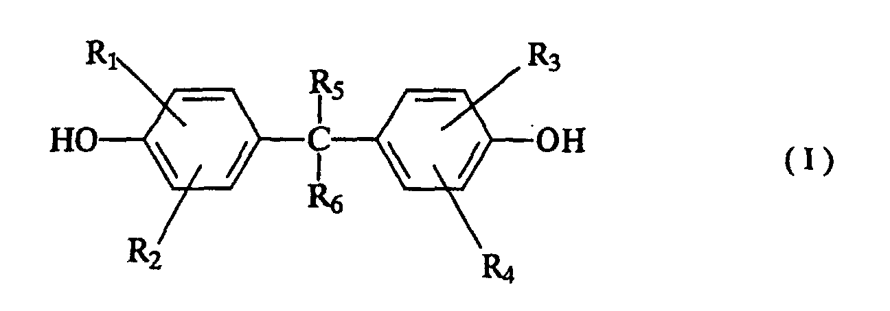
compounds being represented by general formula (I):
wherein R
1 to R
4 each represent a hydrogen atom, a C
1 to C
3 alkyl group
or -CH
2OH whereupon at least one of R
1 to R
4 represents -CH
2OH, and
R
5 and R
6 each represent a hydrogen atom or a C
1 to C
3 alkyl group.
Further, the present invention relates to a method of forming
a reverse tapered resist pattern, wherein the alkali-soluble resin
in the radiation sensitive resin composition is obtained by using
methylol bisphenol compounds represented by general formula (I)
above and phenol compounds in a ratio by weight of from 40 : 60 to
100 : 0.
Further, the present invention relates to a method of forming
a metal film pattern, which comprises forming a metal film over a
reverse tapered resist pattern obtained in the pattern-forming
method described above and then removing the reverse tapered resist
pattern.
Further, the present invention relates to a method of forming
a pattern consisting of a metal film, which comprises forming a metal
film over a reverse tapered resist pattern obtained in the
pattern-forming method described above and using the reverse tapered
resist pattern as an insulating member between metal films.
Further, the present invention relates to an organic
electroluminescent display comprising a reverse tapered barrier
plate member between metal films which is formed from a
negative-working radiation sensitive resin composition containing
an alkali-soluble resin obtained by polycondensation of methylol
bisphenol compounds represented by general formula (I) above, phenol
compounds used as necessary and aldehydes.
DETAILED DESCRIPTION OF THE INVENTION
Hereinafter, the present invention is described in detail.
The above-described negative-working radiation sensitive
resin composition, which is used in the method of forming a resist
pattern or forming a metal film pattern according to the present
invention or used as a material of an insulating member between metal
films in the present invention, comprises preferably (A) an
alkali-soluble resin obtained by polycondensation of methylol
bisphenol compounds represented by general formula (I) above, phenol
compounds used as necessary and aldehydes, (B) a crosslinking agent
and (C) an photo-acid generator generating an acid upon irradiation.
Hereinafter, these materials constituting the negative-working
radiation sensitive resin composition are described in more detail.
(A) Alkali-soluble resin
First, the methylol bisphenol compounds of general formula
(I) above serving as a raw material for the alkali-soluble resin
used in the present invention can be obtained by reacting bisphenols
with formalin in the presence of a basic catalyst and then
precipitating the reaction product with an acid. The bisphenols
include e.g. bisphenols A, B, C, E, F and G, among which bisphenol
A, B or F is particularly preferable. The methylol compound may be
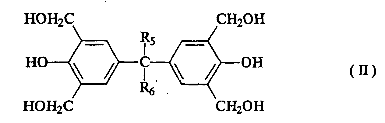
any one of mono-, di-, tri-, and tetra-methylol compounds, but as
compounds represented by the general formula (I), preferably used
are those tetramethylols represented by general formula (II):
wherein R
5 and R
6 each represent a hydrogen atom or a C
1 to C
3 alkyl
group.
An alkali-soluble resin used in the present invention is
obtainable by adding at least one of aldehydes such as formalin
to at least one kind of the methylol bisphenol compounds or a mixture
of the methylol bisphenol compound(s) and at least one of phenol
compounds used as necessary and allowing the mixture to be
polycondensed.
As the phenol compounds to be used for preparing the
alkali-soluble resin, which include phenol compounds in a wide sense
such as phenols, bisphenols and naphtols, there may be illustrated,
for example, phenol, p-cresol, m-cresol, o-cresol, 2,3-dimethylphenol,
2,4-dimethylphenol, 2,5-dimethylphenol, 2,6-dimethylphenol,
3,4-dimethylphenol, 3,5-dimethylphenol, 2,3,4-trimethylphenol,
2,3,5-trimethylphenol, 3,4,5-trimethylphenol,
2,4,5-trimethylphenol, methylene-bisphenol, methylene-bis-p-cresol,
resorcinol, catechol, 2-methylresorcinol, 4-methylresorcinol,
o-chlorophenol, m-chlorophenol, p-chlorophenol,
2,3-dichlorophenol, m-methoxyphenol, p-methoxyphenol, p-butoxyphenol,
o-ethylphenol, m-ethylphenol, p-ethylphenol, 2,3-diethylphenol,
2,5-diethylphenol, p-isopropylphenol,α-naphthol,
β-naphthol, and the like. These are used singly or as a mixture of
two or more thereof.
The proportion (by weight) of the methylol bisphenol compounds
and the phenol compounds used is usually from 40 : 60 to 100 : 0,
preferably from 50 : 50 to 100 : 0, and more preferably from 70 :
30 to 95 : 5, and the weight average molecular weight of the
alkali-soluble resin as determined with polystyrene standards is
preferably from 2,000 to 10,000, more preferably 3,000 to 7,000.
The aldehydes used include arbitrary aldehydes such as
paraformaldehyde and acetaldehyde as well as formalin, and these
can be used singly or as a mixture of two or more thereof. These
aldehydes are used in an amount of 0.6 to 3.0 moles, preferably 0.7
to 1.5 moles, relative to 1 mole of the phenol compounds.
(B) Cross-linking agent
As the cross-linking agent to be used in the present invention,
any compound that causes cross-linking reaction by acid can be used.
Preferable cross-linking agents include alkoxyalkylated amino resin
such as alkoxyalkylated melamine resins, alkoxyalkylated urea resins,
etc. as well as melamine type, guanamine type and urea type compounds.
As specific examples of such alkoxyalkylated amino resins, there
may be illustrated methoxymethylated melamine resin,
ethoxymethylated melamine resin, propoxymethylated melamine resin,
butoxymethylated melamine resin, methoxymethylated urea resin,
ethoxymethylated urea resin, propoxymethylated urea resin,
butoxymethylated urea resin, etc.
These cross-linking agents may be used singly or as a mixture
of two or more thereof, and are compounded in an amount of usually
2 to 50 parts by weight, preferably 5 to 30 parts by weight, relative
to 100 parts by weight of the alkali-soluble resin.
(C) Photo-acid generator
As the photo-acid generator to be used in the present invention,
any one of known or well-known photo-acid generators that have
conventionally been used in a chemically amplified radiation
sensitive resin composition can be used. Examples thereof include
onium salts such as iodonium salts, sulfonium salts, diazonium salts,
ammonium salts, pyridinium salts, etc.; halogen-containing
compounds such as haloalkyl group-containing hydrocarbon compounds,
haloalkyl group-containing heterocyclic compounds, etc.;
diazoketone compounds such as 1,3-diketo-2-diazo compounds,
diazobenzoquinone compounds, diazonaphthoquinone compounds, etc.;
sulfone compounds such as β-ketosulfones, β-sulfonylsulfones, etc.;
and sulfonic acid compounds such as alkylsulfonic acid esters,
haloalkylsulfonic acid esters, arylsulfonic acid esters,
iminosulfonates, etc. These photo-acid generators can be used
singly or as a mixture of two or more thereof and compounded in an
amount of usually 0.1 to 10 parts by weight, preferably 0.5 to 5.0
parts by weight, relative to 100 parts by weight of the alkali-soluble
resin.
The radiation sensitive resin composition of the present
invention is compounded preferably with a basic compound as an
additive. This basic compound can control the phenomenon of
diffusion in the resist film of an acid generated from the photo-acid
generator upon exposure, thus improving resolution, exposure
allowance etc. Examples of such basic compounds include primary,
secondary or tertiary aliphatic amines, aromatic amines,
heterocyclic amines, nitrogenous compounds containing alkyl or aryl
group, compounds containing amide or imide group, etc.
As solvents used in the radiation sensitive resin composition
of the present invention for dissolving the alkali-soluble resin,
cross-linking agent and photo-acid generator, there may be
illustrated ethylene glycol monoalkyl ethers such as ethylene glycol
monomethyl ether, ethylene glycolmonoethyl ether, etc.; ethylene
glycol monoalkyl ether acetates such as ethylene glycol monomethyl
ether acetate, ethylene glycol monoethyl ether acetate, etc.;
propylene glycol monoalkyl ethers such as propylene glycol
monomethyl ether, propylene glycol monoethyl ether, etc.; propylene
glycol monoalkyl ether acetates such as propylene glycol monomethyl
ether acetate, propylene glycol monoethyl ether acetate, etc.;
lactic esters such as methyl lactate, ethyl lactate, etc.; aromatic
hydrocarbons such as toluene, xylene, etc.; ketones such as methyl
ethyl ketone, 2-heptanone, cyclohexanone, etc.; amides such as
N,N-dimethylacetamide, N-methylpyrrolidone, etc.; lactones such as
γ-butyrolactone, etc.; and the like. These solvents are used singly
or in combination of two or more thereof.
The radiation sensitive resin composition of the present
invention may further contain, if necessary, a dye, an adhesion aid,
a surfactant, etc. Examples of the dye include Methyl Violet,
Crystal Violet, Malachite Green, etc., examples of the adhesion aid
include hexamethyldisilazane, chloromethylsilane, etc., and
examples of the surfactant include nonionic surfactants such as
polyglycols and the derivatives thereof, i.e., polypropylene glycol
or polyoxyethylene lauryl ether, fluorine-containing surfactants
such as Fluorad (trade name; made by Sumitomo 3M), Megafac (trade
name; made by Dainippon Ink and Chemicals Inc.), Sulfulon (trade
name; made by Asahi Glass Co., Ltd.) , and organosiloxane surfactants
such as KP341 (trade name; made by Shin-etu Kagaku Kogyo K.K.)
In the present invention, the formation of the reverse tapered
resist pattern by use of these negative-working radiation sensitive
resin compositions is carried out usually in the following manner.
That is, the negative-working radiation sensitive resin composition
is first applied onto a substrate by a coating method known in the
art, such as spin coating, roller coating etc., and then pre-baked
to form a photoresist film. The film is subjected to pattern exposure
and as necessary to post-exposure bake (PEB), followed by development
thereof with an alkali developing solution. By regulating these
conditions, the reverse tapered resist pattern can be obtained. The
reverse cone angle thereof, that is, the angle of the tapered face
of the reverse tapered resist pattern to the substrate, is preferably
75° or less, more preferably 60° or less.
In the present invention, the photoresist film obtained by
applying the negative-working radiation sensitive resin composition
and then pre-baking it may have an arbitrary thickness. However for
use of the reverse tapered resist pattern as e.g. an insulating member
between electrodes in an organic EL panel, the thickness of the film
is preferably about 1 to 10 µm. As a matter of course, the substrate
on which the resist pattern is formed may have electrodes etc. thereon
and have an uneven surface. For exposure, there may be used arbitrary
radiation which is conventionally used for exposure of radiation
sensitive resin compositions, for example ultraviolet rays, deep
ultraviolet rays, electron beam, X rays etc.
Further, the formation of the metal film pattern by the
lift-off method is carried out by forming ametal film on the substrate
by use of as a mask the resist pattern formed described above and
then releasing and removing the resist pattern with a solvent etc.
The releasing agent for the resist includes e.g. AZ Remover 100
(manufactured by Clariant Japan K.K.). The metal constituting the
metal film pattern formed by the present invention may be not only
highly electrically conductive metals such as Al, Cu and Au, but
also metal oxides etc. For formation of the metal film, vacuum-deposition.
sputtering, CVD, ion plating etc. can be used. In this
lift-off method, the metal film formed on the resist is removed
together with the resist upon removal of the resist pattern, whereby
the metal film pattern is formed. By heating the substrate during
vapor deposition etc., the temperature of the resist may raise to
high temperature. The radiation sensitive resin composition,
therefore, is preferably heat-resistant and free from deformation
of the pattern upon heating during vapor deposition.
In case of utilizing the reverse tapered resist pattern formed
described above as e.g. an insulating member between electrodes in
an organic EL panel, an EL medium layer and an electrode layer are
vapor-deposited onto the substrate by using the resist pattern as
a mask. For that reason, a panel is formed in such a state that the
metal layer used for forming electrodes and so on remain on the resist
pattern. To prevent short-circuit between adjacent electrodes, it
is therefore necessary that the metal film allow to be not formed
on the side of the reverse tapered resist pattern upon vapor-deposition
of the metal, and that the reverse cone angle is enough
to prevent short-circuit, while paying an enough attention for the
angle of vapor deposition to an evaporation source. Further, if,
for example, the profile of the reverse tapered pattern has a thin
projection at a surface part of the resist pattern or the reverse
tapered pattern is poor in heat resistance, the resist pattern may
be deformed by rise of temperature thereof during vapor-deposition,
heating of the resist pattern for minimizing release of organic gas
from the barrier plate member, or rise of temperature thereof during
dry etching. As a result, the metal layer on the resist pattern and
the electrode film may be brought into contact with each other to
cause short-circuit between the luminescencent elements. The
important requirements for the resist pattern, therefore, are good
shape and heat resistance. Further, if the water absorption of the
resist is high, water will be generated from the resist constituting
the barrier plate member after formation of an organic EL display
panel, thus shortening the longevity of the organic EL panel. It
is therefore necessary to select a resist material free of these
drawbacks, as described above.
BEST MODE FOR CARRYING OUT THE INVENTION
Hereinafter, the present invention is described in detail by
reference to the Examples, which however are not intended to limit
the present invention.
Synthesis Example (Synthesis of alkali-soluble resin A)
114 g of bisphenol A, 163 g of 37 wt-% formalin and 170 g of
water were charged into a separable flask, and then a solution of
40 g of sodium hydroxide in 40 g of water was added dropwise thereto
through a dropping funnel. After the solution was added, the mixture
was heated to 45 °C and reacted for 8 hours under stirring. After
the reaction was completed, the reaction solution was cooled down
to 15 °C and then subjected to acid precipitation by adding 500 ml
of 2 N hydrochloric acid dropwise thereto through a dropping funnel,
whereby powdery crystals of 2,2-bis(3,5-dihydroxymethyl-4-hydroxyphenyl)
propane were precipitated. These precipitates were
filtered off, washed with water and dried to give 140g of powdery
crystals.
100 parts by weight of a mixture consisting of the
tetramethylol derivative of bisphenol A thus obtained and m-cresol
(weight ratio, 50 : 50) was compounded with 54 parts by weight of
37 wt-% aqueous formaldehyde and 2 parts by weight of oxalic acid,
and the mixture was reacted at a reaction temperature of 100 °C for
5 hours under a nitrogen atmosphere. The molecular weight of
alkali-soluble resin A thus obtained was 6,200 as determined with
polystyrene standards.
Example 1
100 parts by weight of alkali-soluble resin A obtained in the
Synthesis Example, 25 parts by weight of alkoxymethylated
benzoguanamine resin and 2 part by weight of 2,4,6-tris(trichloromethyl)
triazine were dissolved in propylene glycol
monomethyl ether acetate and then filtered through a 0.2 µm Teflon
membrane filter to prepare a negative-working radiation sensitive
resin composition. This composition was spin-coated onto a 4-inch
silicon wafer and then baked on a hot plate at 100°C for 120 seconds
to give a resist film of 3.0 µm in thickness. This resist film was
subjected to exposure by a proximity exposure unit (PL501F, Canon
Inc.) and then to PEB at 100°C for 90 seconds, followed by development
for 90 seconds with 2.38 wt-% aqueous tetramethylammonium hydroxide
solution to form a pattern of 30 µm in width.
The reverse cone angle of the resulting pattern was 50°, and
the resist pattern had a good shape having neither thin projection
at the edges nor hollows on the top.
The formed pattern was further subjected to heat treatment
at a temperature of 300 °C for 60 minutes, and then the shape of the
pattern was observed. In the shape, there was little change to dull
edges, thickened line width, etc., and the reverse cone angle could
be kept at 60°.
Comparative Example 1
A negative-working radiation sensitive resin composition was
prepared and a pattern was formed in the same manner as in Example
1 except that the alkali-soluble resin was formed from mixed cresols
consisting of m-cresol/p-cresol in a ratio of 6/4. The reverse cone
angle of the resulting pattern was 55°, but the edges projected
slightly thinly, and there was a hollow of about 1500 Å in depth
on the top.
The formed pattern was further subjected to heat treatment
at a temperature of 300 °C for 60 minutes, and then the shape of the
pattern was observed. The shape was significantly changed to fail
to keep the reverse tapered shape.
Example 2
A resist film was obtained in the same manner as in Example
1 except that the pattern exposure was conducted by whole image
exposure system and the development time was 60 seconds. The
resulting resist film was subjected to heat treatment at 270 °C for
60 minutes. Further, the resist film was dried at 50 °C for 24 hours
and the weight (M1) of the film was measured. Thereafter, the resist
film was immersed in pure water for 24 hours and then the weight
(M2) of the film was measured again. The saturated water absorption
thereof was 2.72 % as determined from the equation:
Saturated water absorption = ((M2 - M1)/(M1 - W))×100
wherein W is the weight of the wafer.
Comparative Example 2
The water absorption was determined in the same manner as in
Example 2 except that the radiation sensitive resin composition used
was the radiation sensitive resin composition in Comparative Example
1. The water absorption thus determined was 4.63 %, indicating that
the water absorption of the resulting resist pattern was 1.7 times
as high as that of the radiation sensitive resin composition of the
present invention.
As can be seen from the results described above, the radiation
sensitive resin composition used in the present invention can form
a reverse tapered resist pattern with good shape, which is superior
in heat resistance and shows low water absorption. Therefore the
composition can be preferably used not only as a radiation sensitive
resin composition for the lift-off method but also as barrier plate
material between electrodes in organic EL displays.
EFFECT OF THE INVENTION
As described above in detail, a reverse tapered resist pattern
with a good shape can be formed by the pattern-forming method of
using the novel negative-working radiation sensitive resin
composition of the present invention. By virtue of superior heat
resistance, the formed reverse tapered resist pattern permits
formation of a good metal film pattern by the lift-off method, and
by virtue of low water absorption, it can be used preferably as a
barrier plate material between electrodes in organic EL displays.