EP1265343A2 - DC-DC converter - Google Patents
DC-DC converter Download PDFInfo
- Publication number
- EP1265343A2 EP1265343A2 EP02253942A EP02253942A EP1265343A2 EP 1265343 A2 EP1265343 A2 EP 1265343A2 EP 02253942 A EP02253942 A EP 02253942A EP 02253942 A EP02253942 A EP 02253942A EP 1265343 A2 EP1265343 A2 EP 1265343A2
- Authority
- EP
- European Patent Office
- Prior art keywords
- output
- circuit
- signal
- converter
- integrator
- Prior art date
- Legal status (The legal status is an assumption and is not a legal conclusion. Google has not performed a legal analysis and makes no representation as to the accuracy of the status listed.)
- Granted
Links
Images
Classifications
-
- H—ELECTRICITY
- H02—GENERATION; CONVERSION OR DISTRIBUTION OF ELECTRIC POWER
- H02M—APPARATUS FOR CONVERSION BETWEEN AC AND AC, BETWEEN AC AND DC, OR BETWEEN DC AND DC, AND FOR USE WITH MAINS OR SIMILAR POWER SUPPLY SYSTEMS; CONVERSION OF DC OR AC INPUT POWER INTO SURGE OUTPUT POWER; CONTROL OR REGULATION THEREOF
- H02M3/00—Conversion of DC power input into DC power output
- H02M3/02—Conversion of DC power input into DC power output without intermediate conversion into AC
- H02M3/04—Conversion of DC power input into DC power output without intermediate conversion into AC by static converters
- H02M3/10—Conversion of DC power input into DC power output without intermediate conversion into AC by static converters using discharge tubes with control electrode or semiconductor devices with control electrode
- H02M3/145—Conversion of DC power input into DC power output without intermediate conversion into AC by static converters using discharge tubes with control electrode or semiconductor devices with control electrode using devices of a triode or transistor type requiring continuous application of a control signal
- H02M3/155—Conversion of DC power input into DC power output without intermediate conversion into AC by static converters using discharge tubes with control electrode or semiconductor devices with control electrode using devices of a triode or transistor type requiring continuous application of a control signal using semiconductor devices only
- H02M3/156—Conversion of DC power input into DC power output without intermediate conversion into AC by static converters using discharge tubes with control electrode or semiconductor devices with control electrode using devices of a triode or transistor type requiring continuous application of a control signal using semiconductor devices only with automatic control of output voltage or current, e.g. switching regulators
Definitions
- the present invention relates to a DC-DC converter which uses a ⁇ modulator to limit excessive peak current flowing to an inductor and power switching element by monitoring the current flowing to said inductor with an integrator composed with a ⁇ modulator.
- ⁇ modulation is a modulation method in which modulator input signal us integrated, quantization is carried out by comparing the integrated value with a reference voltage, and modulator output signal is fed back to the modulator input.
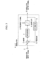
- Fig. 3 is a block drawing of a primary ⁇ modulator. A DC-DC converter that switches power switching element 8 can be produced using this modulation system.
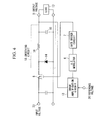
- Fig. 4 shows a step-down chopper DC-DC converter as an example of a method of the prior art that uses ⁇ modulation.
- This DC-DC converter is equipped with smoothing circuit 18, ⁇ modulator 6 is connected to the output side of this smoothing circuit 18 via an error amplification circuit 13, and output side of this ⁇ modulator 6 is connected to the input of power switching element 8 via a gate driver circuit 7.
- a constant voltage output can be obtained by comparing the converter output voltage with a reference voltage, performing ⁇ modulation by using the error amplification signal voltage of the compared voltage as the modulator input signal of ⁇ modulator 6, switching power switching element 8 according to the output signal of modulator 6, and inputting the above switching output to smoothing circuit 18.
- DC-DC converters using a pulse width modulation system which has typically been used in the past, being characterized by the switching frequency being constant
- DC-DC converters using ⁇ modulation are synchronized with the sampling frequency given by the ⁇ modulator, and the output 1 bit signal is changed so that the error between the modulator input signal voltage and modulator output signal voltage becomes minimal. Consequently, the ⁇ modulator input signal voltage changes according to the DC-DC converter output voltage and as a result, this modulation system has the characteristic of the switching frequency changing.
- DC-DC converters have the characteristic that, during the time power switching element 8 is off, current flows through rectifier 14 while capacitor 15 discharges, and due to the presence of inductor 16, current decreases gradually instead of sharply, while during the time power switching element 8 is on, current flows to inductor 16 through power switching element 8, capacitor 15 discharges, and due to the presence of inductor 16, current rises gradually, and the current that flows rises the longer the period during which power switching element 8 is on.
- power loss of power switching element 8 is determined by the product of the on resistance of power switching element 8 and the square of the current flowing to power switching element 8, if the current flowing to power switching element 8 increases, the power loss in power switching element 8 becomes extremely large. Moreover, since the power loss in rectifier 14 is determined by the forward voltage and current that is flowing, and power loss also becomes large when the current flowing to rectifier 14 increases, particularly in cases in which the DC-DC converter output current is large, converters using ⁇ modulation had the problem of poor power conversion efficiency as compared with those using PWM modulation due to the large current flowing inside the converter.
- the object of the present invention is to provide a highly efficient DC-DC converter that uses ⁇ modulation to limit excessive peak current flowing inside the converter by monitoring the current flowing inside the converter with an integrator located inside a ⁇ modulator.
- the present invention for achieving the above object is a DC-DC converter that switches a power switching element by inputting an analog input signal or multi-bit digital signal into a ⁇ modulator, and conveying that modulated signal to the power switching element via a gate driver circuit, wherein excessive peak current flowing to an inductor is limited by monitoring the current flowing inside the converter with an integrator located inside the ⁇ modulator.
- the ⁇ modulator is composed of at least one adder, integrator and quantizer, has a feedback pathway that feeds back from the output of the quantizer to the input of at least one adder, at least one integrator is connected to the output of the adder, and at least one output of the integrator is connected to the quantizer.
- the DC-DC converter is also provided with an adder serving as the input of the ⁇ modulator and an integrator connected to the output of that adder, and an analog adder and analog integrator are used in the case of inputting a continuous time signal in the manner of an analog signal to a modulator, while a digital adder and digital integrator are used in the case of inputting a discrete time signal in the manner of a multi-bit digital signal to a modulator.
- the quantizer performs sampling on the discrete time signal, while the output of this quantizer and the output of a current control circuit, to which is connected the output of the above integrator and the output of an error amplification circuit, are connected to the input of an AND circuit that determines the final pulse width, and the output signal of this AND circuit is connected to the input of a gate driver circuit that supplies current and voltage sufficient for driving the power switching element.
- the output of the above gate driver circuit is connected to the input of a power switching element that switches the input voltage of the DC-DC converter, while the output of the power switching element is connected to a smoothing circuit, and the output of this smoothing circuit becomes the output of the DC-DC converter.
- the above feedback pathway in the ⁇ modulator is equipped with an attenuator that conforms to output signal of the quantizer to the input signal level of the ⁇ modulator.
- an attenuator having an attenuation factor of 0 is also considered to be included in the case the signal level of the quantizer output and the signal level of the ⁇ modulator input are already conforming at the outset, and an attenuator is not required.
- the present invention has a constitution such that, the output of the above integrator and the output of the above error amplifier are compared by the above current control circuit, an excessive peak signal is generated with the output of the above integrator, and when that excessive peak signal has reached the output signal level of the above error amplifier, a pulse signal is output from the current control circuit, and a signal that switches off the power switching element is applied to the power switching element through a gate driver circuit by the above AND circuit after having received the pulse signal output from the current control circuit.
- the present invention makes it possible to suppress excessive peak current flowing within the DC-DC converter, and enables the realization of a highly efficient DC-DC converter.
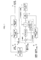
- Fig. 1 shows a block diagram of an embodiment of the present invention.
- the present embodiment is composed so as to detect current flowing to an inductor provided in a smoothing circuit 18 by being equipped with ⁇ modulator 6 and providing an integrator 3 in this ⁇ modulator 6.
- a current control circuit 19 is connected to integrator 3
- an AND circuit 12 is connected to this current control circuit 19 and ⁇ modulator 6, and a power switching element 8 is connected to this AND circuit 12 via a gate driver circuit 7.
- an attenuator 11 is connected to the output of a quantizer 4, and this attenuator 11 is provided with a feedback pathway 10 connected to the input of an adder 2.
- Modulator input signal 1 is input to adder 2, the output of this adder 2 is input to quantizer 4 through integrator 3, the output signal of this quantizer 4 is converted to a 1-bit digital signal synchronized with a frequency signal, and this signal is then input to AND circuit 12.
- modulator input signal 1 and the output signal of adder 3 are compared in current control circuit 19, and that comparison signal is input to AND circuit 12.
- the voltage/current of a signal generated according to the signal input to that AND circuit 12 is then amplified in gate driver circuit 7 and supplied to power switching element 8.
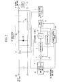
- Fig. 2 is a block diagram in which the present invention is applied to a ⁇ modulation type of step-down chopper.
- This step-down chopper is composed such that the voltage output to load 17 and the differential voltage of reference voltage 20 are amplified by error amplification circuit 13, a pulse applied to power switching element 8 is generated from the pathway in which that differential voltage is input to ⁇ modulator 6 and the modulated signal is input to AND circuit 12, and from the pathway in which that differential voltage and the signal obtained from ⁇ modulator 6 are input to current control circuit 19 and that control signal is input to AND circuit 12, and the pulses generated in that AND circuit 12 are input to gate driver circuit 7 followed by driving power switching element 8 with the output signal of that gate driver circuit 7.
- Input voltage 23 is an analog signal, and for example, if a direct current voltage is input, the output of power switching element 8 is able to obtain a direct current voltage for which the power has been amplified. Namely, this input voltage 23 is able to drive a DC-DC converter according to output voltage 9. Since the signal following modulation is converted to a binary signal, the DC-DC converter can be easily composed in the form of an integrated circuit, thereby making it possible to provide a compact DC-DC converter.
- the pulse signal generated with AND circuit 12 by ⁇ modulator 6 and the signal of current control circuit 19 are applied to power switching element 8 and limit the current flowing to the above inductor in the form of a pulse signal for which the on width is limited when the peak current of the above inductor has reached the threshold value of error amplification circuit 13.
- step-down chopper is described in Fig. 2, the present invention can also clearly be applied to a step-up chopper or polarity inversion chopper by using a similar method.
- a current-limiting ⁇ modulating DC-DC converter can be realized that limits inductor current by having a pathway in which the output signal of integrator 3 and the output signal of error amplification circuit 13 are input to AND circuit 12 through a comparator, a pathway in which the output signal of error amplification circuit 13 is modulated with adder 2, integrator 3 and quantizer 4 and then input to AND circuit 12, and limiting the on width in AND circuit 12 by the signals of these two pathways.
- the former is able to increase sampling accuracy, while the latter is able to accommodate parallel output, thereby making it possible to provide a high-precision, multi-output DC-DC converter in a compact integrated circuit.
Landscapes
- Engineering & Computer Science (AREA)
- Power Engineering (AREA)
- Dc-Dc Converters (AREA)
- Compression, Expansion, Code Conversion, And Decoders (AREA)
- Analogue/Digital Conversion (AREA)
- Amplifiers (AREA)
Abstract
Description
Claims (4)
Applications Claiming Priority (2)
| Application Number | Priority Date | Filing Date | Title |
|---|---|---|---|
| JP2001172624A JP3776752B2 (en) | 2001-06-07 | 2001-06-07 | DC-DC converter |
| JP2001172624 | 2001-06-07 |
Publications (3)
| Publication Number | Publication Date |
|---|---|
| EP1265343A2 true EP1265343A2 (en) | 2002-12-11 |
| EP1265343A3 EP1265343A3 (en) | 2004-04-07 |
| EP1265343B1 EP1265343B1 (en) | 2006-08-16 |
Family
ID=19014213
Family Applications (1)
| Application Number | Title | Priority Date | Filing Date |
|---|---|---|---|
| EP02253942A Expired - Lifetime EP1265343B1 (en) | 2001-06-07 | 2002-06-06 | DC-DC converter |
Country Status (5)
| Country | Link |
|---|---|
| US (1) | US6621257B2 (en) |
| EP (1) | EP1265343B1 (en) |
| JP (1) | JP3776752B2 (en) |
| AT (1) | ATE336823T1 (en) |
| DE (1) | DE60213911T2 (en) |
Cited By (4)
| Publication number | Priority date | Publication date | Assignee | Title |
|---|---|---|---|---|
| US6784648B2 (en) * | 2001-03-08 | 2004-08-31 | Shindengen Electric Manufacturing Co., Ltd. | DC stabilized power supply |
| ES2302407A1 (en) * | 2005-09-30 | 2008-07-01 | Salicru, S.A | AC CURRENT VOLTAGE STABILIZER FOR LIGHTING FACILITIES AND CLOSED LOOP CONTROL PROCEDURE WITH MODULATION BY PULSE EXTENSION. |
| US7852051B2 (en) | 2005-01-18 | 2010-12-14 | Puls Gmbh | Current-limiting circuit and method for operating the circuit |
| DE102005002359C5 (en) * | 2005-01-18 | 2015-10-29 | Puls Gmbh | Current limiting circuit and method of operating the circuit |
Families Citing this family (14)
| Publication number | Priority date | Publication date | Assignee | Title |
|---|---|---|---|---|
| JP3610950B2 (en) * | 2002-01-11 | 2005-01-19 | 日産自動車株式会社 | Power supply |
| JP4791689B2 (en) * | 2003-10-06 | 2011-10-12 | パナソニック株式会社 | Power supply |
| KR100576373B1 (en) * | 2004-03-08 | 2006-05-03 | 학교법인 한양학원 | Digital DC-DC Converters Using Digital Modulation Techniques |
| JP4254674B2 (en) * | 2004-09-28 | 2009-04-15 | アイシン精機株式会社 | Antenna drive device |
| JP4898343B2 (en) * | 2006-08-09 | 2012-03-14 | パナソニック株式会社 | Power supply |
| DE102007053874B3 (en) * | 2007-11-09 | 2009-04-09 | Atmel Germany Gmbh | Monolithic integrated circuit and use of a semiconductor switch |
| US7773016B2 (en) * | 2008-09-29 | 2010-08-10 | Analog Devices, Inc. | Switching converters controlled via sigma delta modulation |
| JP2012080670A (en) * | 2010-10-01 | 2012-04-19 | Elpida Memory Inc | Switching regulator |
| EP2451062B1 (en) * | 2010-11-08 | 2018-10-24 | Nxp B.V. | PFC with multi-channel error feedback |
| US8823346B2 (en) | 2011-12-09 | 2014-09-02 | Intersil Americas LLC | System and method of feed forward for boost converters with improved power factor and reduced energy storage |
| BE1020014A5 (en) * | 2012-01-27 | 2013-03-05 | Mindcet Bvba | METHODS AND SYSTEM FOR CALCULATING MODEL PARAMETERS FOR A SPOOL TO BE MODELED. |
| US9389628B2 (en) * | 2012-04-20 | 2016-07-12 | Intel Deutschland Gmbh | Digitally controlled buck-boost regulator having a custom mapping controller |
| US9780675B2 (en) | 2015-12-11 | 2017-10-03 | General Electric Company | System and method for controlling current in a power converter |
| JP7668953B2 (en) * | 2022-03-03 | 2025-04-25 | 三菱電機株式会社 | Analog/digital converter, analog/digital conversion system, digital control device, and digitally controlled power supply |
Family Cites Families (10)
| Publication number | Priority date | Publication date | Assignee | Title |
|---|---|---|---|---|
| US5479090A (en) * | 1993-11-24 | 1995-12-26 | Raytheon Company | Power converter having optimal dynamic operation |
| JPH07254823A (en) * | 1994-03-14 | 1995-10-03 | Kenwood Corp | Delta sigma modulation amplifier |
| US6191676B1 (en) * | 1994-10-21 | 2001-02-20 | Spinel Llc | Apparatus for suppressing nonlinear current drawing characteristics |
| US5677618A (en) * | 1996-02-26 | 1997-10-14 | The Boeing Company | DC-to-DC switching power supply utilizing a delta-sigma converter in a closed loop controller |
| US5777512A (en) | 1996-06-20 | 1998-07-07 | Tripath Technology, Inc. | Method and apparatus for oversampled, noise-shaping, mixed-signal processing |
| US6154161A (en) * | 1998-10-07 | 2000-11-28 | Atmel Corporation | Integrated audio mixer |
| US6246215B1 (en) * | 1999-03-08 | 2001-06-12 | O2 Micro International Limited | Buffer battery power supply system |
| JP3454186B2 (en) * | 1999-05-14 | 2003-10-06 | 株式会社日立製作所 | Power converter |
| US6404655B1 (en) * | 1999-12-07 | 2002-06-11 | Semikron, Inc. | Transformerless 3 phase power inverter |
| US6448745B1 (en) * | 2002-01-08 | 2002-09-10 | Dialog Semiconductor Gmbh | Converter with inductor and digital controlled timing |
-
2001
- 2001-06-07 JP JP2001172624A patent/JP3776752B2/en not_active Expired - Fee Related
-
2002
- 2002-06-06 EP EP02253942A patent/EP1265343B1/en not_active Expired - Lifetime
- 2002-06-06 DE DE60213911T patent/DE60213911T2/en not_active Expired - Fee Related
- 2002-06-06 AT AT02253942T patent/ATE336823T1/en not_active IP Right Cessation
- 2002-06-07 US US10/163,410 patent/US6621257B2/en not_active Expired - Fee Related
Cited By (5)
| Publication number | Priority date | Publication date | Assignee | Title |
|---|---|---|---|---|
| US6784648B2 (en) * | 2001-03-08 | 2004-08-31 | Shindengen Electric Manufacturing Co., Ltd. | DC stabilized power supply |
| US7852051B2 (en) | 2005-01-18 | 2010-12-14 | Puls Gmbh | Current-limiting circuit and method for operating the circuit |
| DE102005002359C5 (en) * | 2005-01-18 | 2015-10-29 | Puls Gmbh | Current limiting circuit and method of operating the circuit |
| ES2302407A1 (en) * | 2005-09-30 | 2008-07-01 | Salicru, S.A | AC CURRENT VOLTAGE STABILIZER FOR LIGHTING FACILITIES AND CLOSED LOOP CONTROL PROCEDURE WITH MODULATION BY PULSE EXTENSION. |
| ES2302407B1 (en) * | 2005-09-30 | 2009-02-16 | Salicru, S.A | AC CURRENT VOLTAGE STABILIZER FOR LIGHTING FACILITIES AND CLOSED LOOP CONTROL PROCEDURE WITH MODULATION BY PULSE WIDTH. |
Also Published As
| Publication number | Publication date |
|---|---|
| DE60213911T2 (en) | 2007-03-08 |
| US20020185995A1 (en) | 2002-12-12 |
| US6621257B2 (en) | 2003-09-16 |
| JP2002369503A (en) | 2002-12-20 |
| EP1265343B1 (en) | 2006-08-16 |
| DE60213911D1 (en) | 2006-09-28 |
| JP3776752B2 (en) | 2006-05-17 |
| EP1265343A3 (en) | 2004-04-07 |
| ATE336823T1 (en) | 2006-09-15 |
Similar Documents
| Publication | Publication Date | Title |
|---|---|---|
| EP1265343B1 (en) | DC-DC converter | |
| US6653960B2 (en) | Stabilized power supply using delta sigma modulator | |
| US5099203A (en) | Power amplifier having multiple switched stages and method of operating same | |
| US5959443A (en) | Controller circuit for controlling a step down switching regulator operating in discontinuous conduction mode | |
| US7034513B2 (en) | Power supply having efficient low power standby mode | |
| EP1137162B1 (en) | Analog/digital PWM control circuit of a winding | |
| US6100675A (en) | Switching regulator capable of increasing regulator efficiency under light load | |
| US7595623B2 (en) | Methods and apparatus for a spread spectrum switching regulator | |
| US6507504B2 (en) | Method of controlling DC/DC converter for reducing power consumption | |
| EP1469594A1 (en) | Multi level Class-D amplifier by means of 2 physical layers | |
| EP1418667A1 (en) | Multi-level class-D amplifier by means of 3 physical levels | |
| CN103236791B (en) | PWM power converter with improved dynamic response and its control method | |
| US11018581B2 (en) | Methods and devices for operating converters | |
| EP1187303B1 (en) | PWM Control circuit for DC-DC converter | |
| JPH11178329A (en) | Current mode switching converter | |
| EP1406372A1 (en) | Digital control apparatus for a switching DC-DC converter | |
| US7250744B2 (en) | Quasi average current mode control scheme for switching power converter | |
| AU654786B2 (en) | Amplifier with multiple switched stages and noise suppression | |
| US6650099B2 (en) | Switching power supply | |
| JP4380933B2 (en) | Switching signal control circuit | |
| US6812681B1 (en) | Digital dynamic trace adjustment pulse width modulate controller | |
| JP2002300772A (en) | Switching power supply | |
| JP4425029B2 (en) | Switching regulator | |
| JP3776738B2 (en) | Switching signal generator | |
| TW202524830A (en) | Switching converter circuit capable of preventing burst pulses |
Legal Events
| Date | Code | Title | Description |
|---|---|---|---|
| PUAI | Public reference made under article 153(3) epc to a published international application that has entered the european phase |
Free format text: ORIGINAL CODE: 0009012 |
|
| AK | Designated contracting states |
Kind code of ref document: A2 Designated state(s): AT BE CH CY DE DK ES FI FR GB GR IE IT LI LU MC NL PT SE TR |
|
| AX | Request for extension of the european patent |
Free format text: AL;LT;LV;MK;RO;SI |
|
| PUAL | Search report despatched |
Free format text: ORIGINAL CODE: 0009013 |
|
| AK | Designated contracting states |
Kind code of ref document: A3 Designated state(s): AT BE CH CY DE DK ES FI FR GB GR IE IT LI LU MC NL PT SE TR |
|
| AX | Request for extension of the european patent |
Extension state: AL LT LV MK RO SI |
|
| 17P | Request for examination filed |
Effective date: 20040819 |
|
| AKX | Designation fees paid |
Designated state(s): AT BE CH CY DE DK ES FI FR GB GR IE IT LI LU MC NL PT SE TR |
|
| 17Q | First examination report despatched |
Effective date: 20050121 |
|
| GRAP | Despatch of communication of intention to grant a patent |
Free format text: ORIGINAL CODE: EPIDOSNIGR1 |
|
| GRAS | Grant fee paid |
Free format text: ORIGINAL CODE: EPIDOSNIGR3 |
|
| GRAA | (expected) grant |
Free format text: ORIGINAL CODE: 0009210 |
|
| AK | Designated contracting states |
Kind code of ref document: B1 Designated state(s): AT BE CH CY DE DK ES FI FR GB GR IE IT LI LU MC NL PT SE TR |
|
| PG25 | Lapsed in a contracting state [announced via postgrant information from national office to epo] |
Ref country code: IT Free format text: LAPSE BECAUSE OF FAILURE TO SUBMIT A TRANSLATION OF THE DESCRIPTION OR TO PAY THE FEE WITHIN THE PRESCRIBED TIME-LIMIT;WARNING: LAPSES OF ITALIAN PATENTS WITH EFFECTIVE DATE BEFORE 2007 MAY HAVE OCCURRED AT ANY TIME BEFORE 2007. THE CORRECT EFFECTIVE DATE MAY BE DIFFERENT FROM THE ONE RECORDED. Effective date: 20060816 Ref country code: CH Free format text: LAPSE BECAUSE OF FAILURE TO SUBMIT A TRANSLATION OF THE DESCRIPTION OR TO PAY THE FEE WITHIN THE PRESCRIBED TIME-LIMIT Effective date: 20060816 Ref country code: LI Free format text: LAPSE BECAUSE OF FAILURE TO SUBMIT A TRANSLATION OF THE DESCRIPTION OR TO PAY THE FEE WITHIN THE PRESCRIBED TIME-LIMIT Effective date: 20060816 Ref country code: NL Free format text: LAPSE BECAUSE OF FAILURE TO SUBMIT A TRANSLATION OF THE DESCRIPTION OR TO PAY THE FEE WITHIN THE PRESCRIBED TIME-LIMIT Effective date: 20060816 Ref country code: AT Free format text: LAPSE BECAUSE OF FAILURE TO SUBMIT A TRANSLATION OF THE DESCRIPTION OR TO PAY THE FEE WITHIN THE PRESCRIBED TIME-LIMIT Effective date: 20060816 Ref country code: FI Free format text: LAPSE BECAUSE OF FAILURE TO SUBMIT A TRANSLATION OF THE DESCRIPTION OR TO PAY THE FEE WITHIN THE PRESCRIBED TIME-LIMIT Effective date: 20060816 |
|
| REG | Reference to a national code |
Ref country code: GB Ref legal event code: FG4D |
|
| REG | Reference to a national code |
Ref country code: CH Ref legal event code: EP |
|
| REG | Reference to a national code |
Ref country code: IE Ref legal event code: FG4D |
|
| REF | Corresponds to: |
Ref document number: 60213911 Country of ref document: DE Date of ref document: 20060928 Kind code of ref document: P |
|
| PG25 | Lapsed in a contracting state [announced via postgrant information from national office to epo] |
Ref country code: DK Free format text: LAPSE BECAUSE OF FAILURE TO SUBMIT A TRANSLATION OF THE DESCRIPTION OR TO PAY THE FEE WITHIN THE PRESCRIBED TIME-LIMIT Effective date: 20061116 Ref country code: SE Free format text: LAPSE BECAUSE OF FAILURE TO SUBMIT A TRANSLATION OF THE DESCRIPTION OR TO PAY THE FEE WITHIN THE PRESCRIBED TIME-LIMIT Effective date: 20061116 |
|
| PG25 | Lapsed in a contracting state [announced via postgrant information from national office to epo] |
Ref country code: ES Free format text: LAPSE BECAUSE OF FAILURE TO SUBMIT A TRANSLATION OF THE DESCRIPTION OR TO PAY THE FEE WITHIN THE PRESCRIBED TIME-LIMIT Effective date: 20061127 |
|
| PG25 | Lapsed in a contracting state [announced via postgrant information from national office to epo] |
Ref country code: PT Free format text: LAPSE BECAUSE OF FAILURE TO SUBMIT A TRANSLATION OF THE DESCRIPTION OR TO PAY THE FEE WITHIN THE PRESCRIBED TIME-LIMIT Effective date: 20070116 |
|
| NLV1 | Nl: lapsed or annulled due to failure to fulfill the requirements of art. 29p and 29m of the patents act | ||
| REG | Reference to a national code |
Ref country code: CH Ref legal event code: PL |
|
| ET | Fr: translation filed | ||
| PLBE | No opposition filed within time limit |
Free format text: ORIGINAL CODE: 0009261 |
|
| STAA | Information on the status of an ep patent application or granted ep patent |
Free format text: STATUS: NO OPPOSITION FILED WITHIN TIME LIMIT |
|
| 26N | No opposition filed |
Effective date: 20070518 |
|
| PG25 | Lapsed in a contracting state [announced via postgrant information from national office to epo] |
Ref country code: MC Free format text: LAPSE BECAUSE OF NON-PAYMENT OF DUE FEES Effective date: 20070630 |
|
| PG25 | Lapsed in a contracting state [announced via postgrant information from national office to epo] |
Ref country code: GR Free format text: LAPSE BECAUSE OF FAILURE TO SUBMIT A TRANSLATION OF THE DESCRIPTION OR TO PAY THE FEE WITHIN THE PRESCRIBED TIME-LIMIT Effective date: 20061117 |
|
| PG25 | Lapsed in a contracting state [announced via postgrant information from national office to epo] |
Ref country code: IE Free format text: LAPSE BECAUSE OF NON-PAYMENT OF DUE FEES Effective date: 20070606 |
|
| PGFP | Annual fee paid to national office [announced via postgrant information from national office to epo] |
Ref country code: BE Payment date: 20080627 Year of fee payment: 7 |
|
| PGFP | Annual fee paid to national office [announced via postgrant information from national office to epo] |
Ref country code: DE Payment date: 20080626 Year of fee payment: 7 |
|
| PGFP | Annual fee paid to national office [announced via postgrant information from national office to epo] |
Ref country code: FR Payment date: 20080625 Year of fee payment: 7 Ref country code: IT Payment date: 20080627 Year of fee payment: 7 |
|
| PGFP | Annual fee paid to national office [announced via postgrant information from national office to epo] |
Ref country code: GB Payment date: 20080620 Year of fee payment: 7 |
|
| PG25 | Lapsed in a contracting state [announced via postgrant information from national office to epo] |
Ref country code: LU Free format text: LAPSE BECAUSE OF NON-PAYMENT OF DUE FEES Effective date: 20070606 Ref country code: CY Free format text: LAPSE BECAUSE OF FAILURE TO SUBMIT A TRANSLATION OF THE DESCRIPTION OR TO PAY THE FEE WITHIN THE PRESCRIBED TIME-LIMIT Effective date: 20060816 |
|
| PG25 | Lapsed in a contracting state [announced via postgrant information from national office to epo] |
Ref country code: TR Free format text: LAPSE BECAUSE OF FAILURE TO SUBMIT A TRANSLATION OF THE DESCRIPTION OR TO PAY THE FEE WITHIN THE PRESCRIBED TIME-LIMIT Effective date: 20060816 |
|
| BERE | Be: lapsed |
Owner name: *SHINDENGEN ELECTRIC MFG CY LTD Effective date: 20090630 |
|
| GBPC | Gb: european patent ceased through non-payment of renewal fee |
Effective date: 20090606 |
|
| REG | Reference to a national code |
Ref country code: FR Ref legal event code: ST Effective date: 20100226 |
|
| PG25 | Lapsed in a contracting state [announced via postgrant information from national office to epo] |
Ref country code: FR Free format text: LAPSE BECAUSE OF NON-PAYMENT OF DUE FEES Effective date: 20090630 |
|
| PG25 | Lapsed in a contracting state [announced via postgrant information from national office to epo] |
Ref country code: GB Free format text: LAPSE BECAUSE OF NON-PAYMENT OF DUE FEES Effective date: 20090606 |
|
| PG25 | Lapsed in a contracting state [announced via postgrant information from national office to epo] |
Ref country code: DE Free format text: LAPSE BECAUSE OF NON-PAYMENT OF DUE FEES Effective date: 20100101 Ref country code: BE Free format text: LAPSE BECAUSE OF NON-PAYMENT OF DUE FEES Effective date: 20090630 |
|
| PG25 | Lapsed in a contracting state [announced via postgrant information from national office to epo] |
Ref country code: IT Free format text: LAPSE BECAUSE OF NON-PAYMENT OF DUE FEES Effective date: 20090606 |