EP1265123A2 - Clock divider - Google Patents
Clock divider Download PDFInfo
- Publication number
- EP1265123A2 EP1265123A2 EP02253723A EP02253723A EP1265123A2 EP 1265123 A2 EP1265123 A2 EP 1265123A2 EP 02253723 A EP02253723 A EP 02253723A EP 02253723 A EP02253723 A EP 02253723A EP 1265123 A2 EP1265123 A2 EP 1265123A2
- Authority
- EP
- European Patent Office
- Prior art keywords
- circuit
- clocked
- clock signal
- coupled
- clock
- Prior art date
- Legal status (The legal status is an assumption and is not a legal conclusion. Google has not performed a legal analysis and makes no representation as to the accuracy of the status listed.)
- Ceased
Links
Images



Classifications
-
- G—PHYSICS
- G06—COMPUTING OR CALCULATING; COUNTING
- G06F—ELECTRIC DIGITAL DATA PROCESSING
- G06F1/00—Details not covered by groups G06F3/00 - G06F13/00 and G06F21/00
- G06F1/04—Generating or distributing clock signals or signals derived directly therefrom
- G06F1/08—Clock generators with changeable or programmable clock frequency
Definitions
- This invention relates to electronic circuits, and more particularly, but not exclusively, clock divider circuits.
- Production of the different clock signals may be accomplished in various ways. In some cases, separate crystal oscillators may be used to produce the different clock signals. In other cases, it may be desirable use a signal crystal oscillator, or other clock source, along with clock divider and/or multiplier circuitry. For example, if implementing a divide by four circuit, a typical approach may include the use of a first divide by two circuit as an input stage to generate a clock (clk) and a complementary signal, clock bar (!clk). The divide by two circuits may be implemented using D-type flip-flops. The clk and !clk signals from the input stage may then be forwarded to separate divide by two circuits. The outputs of the separate divide by two circuits may be phase shifted by 90° from each other, which may be useful for producing additional clock signals.
- a first divide by two circuit as an input stage to generate a clock (clk) and a complementary signal, clock bar (!clk).
- the divide by two circuits may be implemented using
- a reset or other control signal is normally used to initialize the circuit to a state which provides a predetermined phase shift of one signal from the other.
- the clock divider circuit may include a set of clocked circuits coupled to receive an input clock signal and a complement of the input clock signal.
- the clocked circuits may produce a first output clock signal and a second output clock signal that is phase shifted approximately a positive 90° with respect to the first output clock signal.
- the clock divider circuit may be responsive only to the input clock signal. In other words, the clock divider circuit may not require a reset signal or other type of control signal in order to provide a predictable positive 90° phase shift.
- the clock signals may also have approximately a 50% duty cycle.
- the clock divider circuit may include a series coupled set of input circuits coupled to receive a clock signal and configured to generate the input clock signal and its complement.
- the clock divider circuit may include a pair of cross-coupled divide by two circuits.
- the divide by two circuits may include a plurality of clocked circuits which are configured to pass an input to an output on one phase of the clock cycle, and isolate the output from the input on another phase of the clock cycle.
- the clocked circuits may be passgates.
- the clocked circuits may be transparent during different phases of the clock cycle.
- a divide-by-4 circuit may include four passgates, two of which may be transparent during a clock phase opposite of that for which the other two passgates are transparent. This may result in a pair of output clock signals, wherein a designated one of the output clock signals has approximately a positive 90° phase shift with respect to the other clock signal.
- the output clock signals may also have duty cycle which closely approximates 50% (e.g. about 0.1% error may be experienced in one implementation).
- FIG. 1 a schematic diagram of one embodiment of a clock divider circuit 50 is shown. Other embodiments of the clock divider circuit are possible and contemplated.
- clock divider circuit 50 is a divide by four circuit.
- Clock divider circuit 50 includes an input circuit 52, a plurality of inverters 54A-54E, and a plurality of clocked circuits (PG1, PG2, PG3, and PG4).
- Input circuit 52 includes a pair of series-coupled inverters, and is configured to produce a clock signal, clk , and a complementary clock signal, clk . It is noted that the clock signal and complementary clock signal may be generated in any fashion, as desired.
- the clock signal and its complement may be coupled to clocked circuits PG1-PG4.
- the clocked circuits PG1-PG4 include passgates.
- any clocked circuits which are transparent during one phase of the clock and isolate the input from the output during another phase of the clock may be used (e.g. latches).
- the clock divider circuit 50 includes a plurality of inverters 54A-54E. More particularly, an odd number of inverters 54A-54E may be included in the ring formed by the connections between the passgates. Using an odd number of inverters may cause the circuit to oscillate. Additionally, use of the clocked circuits PG1-PG4 clocked by the input clock signal may cause the oscillation to occur at a frequency determined by the input clock signal.
- Passgates PG1 and PG3 are turned on when the signal clk is asserted, and are transparent at this time (i.e. the input of the passgate is allowed to pass to the output). During this phase of the clk signal, passgates PG3 and PG4 are off, and are thus isolate their inputs from their respective outputs (i.e. the input to the passgate is not allowed to pass to the output). When the clk signal is de-asserted, passgates PG3 and PG4 are turned on, and thus transparent, while passgates PG1 and PG2 are turned off, and thus non-transparent.
- An inverter 54A is coupled between the output of passgate PG2 (node N1) and the input to passgate PG1.
- an inverter 54B is coupled between the output of passgate PG3 (node N4) and the input to passgate PG2;
- an inverter 54C is coupled between the output of passgate PG1 (node N2) and the input of passgate PG4; and
- a pair of series coupled inverters 54D-54E are coupled between the output of passgate PG4 (node N3) and the input to passgate PG3.
- the embodiment of the clock divider circuit 50 illustrated in Figure 1 is a divide by four circuit.
- the output clock signals (out0 and out90) produced by this embodiment of clock divider circuit have a frequency that is one fourth of the frequency of the input clock. The propagation of a single transition through the loop occurs over two input clock cycles.
- a transition (logic 0 to logic 1 or logic 1 to logic 0) at node N1 propagates (inverted) to node N2 during the high phase of a first clock cycle, then from node N2 to N3 (inverted) during the low phase of the first clock cycle, then from node N3 to N4 in the high phase of a second clock cycle, and finally from node N4 to N1 (inverted) during the low phase of the second clock cycle.
- two transitions of the output clocks out0 and out90 occur over a total of four input clock cycles. Since there is an odd number of inverters in the loop, a transition propagates through the loop and arrives back at its initial node as a transition in the opposite direction, and thus the circuit oscillates. With the arrangement of circuits PG1-PG4 clocked by the input clock signal, the oscillation occurs at a quarter of the input clock frequency.
- the configuration of the circuit may allow the first output clock signal (out0) to lead the second output clock signal (out90) by approximately 90° (where a small amount of error may occur due to device mismatch), regardless of the initial conditions of the circuit at start-up.
- a transition on node N1 (which is reflected on out0 through output inverter 56A) propagates to the same transition on node N3 one clock cycle of the input clock signal later (i.e. a transition on N1 occurs during the low phase of a clock cycle of the input clock, is inverted and propagated to node N2 during the following high clock phase of the input clock signal, and then is inverted again and propagated to node N3 during the following low phase of the input clock signal).
- the clock signal out90 lags the clock signal out0 by one clock cycle of the input clock signal. Since the clock divider circuit 50 is a divide by four circuit, the one clock cycle of the input clock signal is one fourth of the output clock cycle, which is 90° of positive phase shift from out0 to out90.
- a divide by eight circuit which includes eight passgates coupled in a ring, with an inverter coupled between successive passgates in the ring (and one link between passgates having two series coupled inverters to provide an odd number of inverters in the ring).
- the divide by eight circuit may produce a 90° phase shift by coupling the out90 output to a node four passgates downstream from the output out0 (i.e. the node to which the out90 output is coupled may receive a transition which occurs on the node to which the out0 output is coupled two clock cycles of the input clock signal, which is one quarter of the output clock cycles of the divide by eight circuit).
- phase shift generated by various embodiments of the clock divider circuit 50 may be varied by changing the node from which the output clock signals are taken. Since transitions flow from node to node responsive to phases of the input clock signal, the phase shift generated may be predetermined based on the number of clock phases which occur between the selected nodes and the number of inversions which occur between the two nodes. The predetermined phase shift may be generated independent of the initial condition of the circuit when powered up, and thus no reset or other control signals may be required to generate the desired phase shift.
- the clock divider circuit 50 may be viewed as a pair of cross-coupled divide by two circuits.
- the passgates PG1 and PG4 and the inverter 54C may be a first divide by two circuit (if the output of the passgate PG4 were coupled to the input of the passgate PG1).
- the passgates PG3 and PG2 and the inverter 54B may be a divide by two circuit (if the output of the passgate PG2 were coupled to the input of the passgate PG3).
- the output of the first divide by two circuit is coupled as the input to the second divide by two circuit and the output of the second divide by two circuit is coupled as the input of the first divide by two circuit.
- the output of the first divide by two circuit (node N3) is coupled to the input of the second divide by two circuit through a pair of inverters 54D-54E and the output of the second divide by two circuit (node N1) is coupled to the input of the first divide by two circuit through an inverter 54A.
- phase shift and the duty cycle may not be exactly 50% and 90°.
- process variations may lead to mismatches in the propagation delay through the inverter 56A which drives out0 with respect the inverter 56B that drives out90, and thus the phase shift may be slightly greater or less than 90°.
- other process variations in the various circuit elements may cause the duty cycle to be slightly greater or less than 50%.
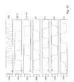
- Figures 2A, 2B, and 2C are timing diagrams illustrating the timing relationships between the various circuit nodes for the embodiment of clock divider circuit 50 illustrated in Figure 1. The results shown were obtained from simulation of the circuit using circuit simulation software. The initial conditions were varied for each of these simulation runs.
- the initial conditions include nodes N1-N4 all being a logic zero and the clock signal, clk , beginning at a logic 0 and transitioning to a logic 1.
- the clock signal then begins its normal transitions. Within a few transitions of the input clock signal, the nodes in the ring are oscillating at one quarter of the input clock frequency.
- Figure 2B illustrates the operation of the circuit with a different set of initial conditions.
- the initial conditions for the circuit for this simulation run are N1 low, N2 low, N3 low, and N4 high, with clk initially held low.
- Figure 2C shows the circuit exhibiting the same pattern of operation, despite yet another set of initial conditions (N1 low, N2 low, N3 high, N4 low).
- the circuit exhibits the same timing relationships after the input clock signal begins its normal cycle and a short settling time.
- simulation results for each set of initial conditions of the nodes N1-N4 and the input clock signal have shown that clock divider circuit 50 operates in a similar manner to that shown in Figures 2A, 2B, and 2C, regardless of the initial conditions.
- a carrier medium 300 including a database representative of clock divider circuit 50 may include storage media such as magnetic or optical media, e.g., disk or CD-ROM, volatile or non-volatile memory media such as RAM (e.g. SDRAM, RDRAM, SRAM, etc.), ROM, etc., as well as transmission media or signals such as electrical, electromagnetic, or digital signals, conveyed via a communication medium such as a network and/or a wireless link.
- storage media such as magnetic or optical media, e.g., disk or CD-ROM, volatile or non-volatile memory media such as RAM (e.g. SDRAM, RDRAM, SRAM, etc.), ROM, etc.
- RAM e.g. SDRAM, RDRAM, SRAM, etc.
- ROM etc.
- transmission media or signals such as electrical, electromagnetic, or digital signals
- the database of clock divider circuit 50 carried on carrier medium 300 may be a database which can be read by a program and used, directly or indirectly, to fabricate the hardware comprising clock divider circuit 50.
- the database may be a behavioral-level description or register-transfer level (RTL) description of the hardware functionality in a high level design language (HDL) such as Verilog or VHDL.
- the description may be read by a synthesis tool which may synthesize the description to produce a netlist comprising a list of gates from a synthesis library.
- the netlist comprises a set of gates which also represent the functionality of the hardware comprising clock divider circuit 50.
- the netlist may then be placed and routed to produce a data set describing geometric shapes to be applied to masks.
- the masks may then be used in various semiconductor fabrication steps to produce a semiconductor circuit or circuits corresponding to clock divider circuit 50.
- the database on carrier medium 300 may be the netlist (with or without the synthesis library) or the data set, as desired.
- carrier medium 300 carries a representation of clock divider circuit 50
- other embodiments may carry a representation of any portion of clock divider circuit 50, as desired.
- the databases referred to above may comprise a circuit defining mechanism for the clock divider circuit and/or portions thereof.
Landscapes
- Engineering & Computer Science (AREA)
- Theoretical Computer Science (AREA)
- Physics & Mathematics (AREA)
- General Engineering & Computer Science (AREA)
- General Physics & Mathematics (AREA)
- Manipulation Of Pulses (AREA)
Abstract
Description
Claims (17)
- A clock divider circuit comprising:wherein the plurality of clocked circuits are configured to output a first clock signal and a second clock signal, responsive only to the input clock signal, and wherein the second clock signal has a predetermined phase shift with respect to the first clock signal.a plurality of clocked circuits coupled to receive an input clock signal, wherein the plurality of clocked circuits are coupled in a ring, wherein at least one inverter is coupled between successive clocked circuits in the ring, and wherein the clock divider circuit includes an odd total number of the inverters in the ring;
- The clock divider circuit as recited in claim 1 wherein the predetermined phase shift is about a positive ninety degrees.
- The clock divider circuit as recited in claim 1 or 2, wherein each of the plurality of clocked circuits includes a passgate.
- The clock divider circuit as recited in claim 3 wherein the passgates within successive clocked circuits are coupled to the input clock signal to be transparent during opposite phases of the input clock signal.
- A clock divider circuit comprising:a pair of cross-coupled divide by two circuits, wherein an output of a first divide by two circuit is a first clock signal and the output of a second divide by two circuit is a second clock signal having about a positive ninety degree phase shift with respect to the first clock signal.
- The clock divider circuit as recited in claim 5, wherein the output of the first divide by two circuit is coupled through an inverter to the input of the second divide by two circuit.
- The clock divider circuit as recited in claim 6, wherein the output of the second divide by two circuit is coupled through a pair of series coupled inverters to the input of the second divide by two circuit.
- A clock divider circuit comprising:a first clocked circuit coupled to receive an input clock signal and configured to be transparent during a first phase of the input clock signal;a second clocked circuit coupled to receive the input clock signal and configured to be transparent during a second phase of the input clock signal;a third clocked circuit coupled to receive the input clock signal and configured to be transparent during the first phase of the input clock signal;a fourth clocked circuit coupled to receive the input clock signal and configured to be transparent during the second phase of the input clock signal;a first inverter coupled between the first clocked circuit and the second clocked circuit;a second inverter coupled between the second clocked circuit and the third clocked circuit;a third inverter coupled between the third clocked circuit and the fourth clocked circuit; anda fourth inverter and a fifth inverter coupled in series between the fourth clocked circuit and the first clocked circuit.
- The clock divider circuit as recited in claim 8 wherein each of the first clocked circuit, the second clocked circuit, the third clocked circuit, and the fourth clocked circuit includes a passgate.
- The clock divider circuit as recited in claim 8 or 9 comprising a sixth inverter coupled to the first clocked circuit and a seventh inverter coupled to the third clocked circuit, the output of the sixth inverter being a first clock output of the clock divider circuit and the output of the seventh inverter being a second clock output of the clock divider circuit.
- The clock divider circuit as recited in claim 10 wherein the second clock output as a predetermined phase shift with respect to the first clock output of about 90 degrees.
- A circuit defining mechansim comprising one or more databases representing one or more of the clock divider circuits as recited in any of claims 1-11.
- The circuit defining mechanism as recited in claim 12 wherein the one or more databases comprise one or more netlists.
- A carrier medium carrying the circuit defining mechanism as recited in any of claims 12-13.
- A computer program comprising machine or computer-readable program elements for configuring a computer to implement the circuit defining mechanism of claim 12 or 13.
- A computer program product comprising a computer usable medium having machine or computer-readable program elements embodied in said computer usable medium operable to effect the performance of defining a circuit, said computer readable program code comprising computer readable program code for causing at least one computer to implement the circuit delivering mechanism of claim 12 or 13.
- The carrier medium of claim 14 or computer program product of claim 16, wherein the carrier medium or computer usable medium comprises at least one of the following set of media: a signal including an optical, electronic or r.f. signal, a magnetic disk or tape, solid-state memory, an optical readable and/or writable disk, a compact disk and a digital versatile disk.
Applications Claiming Priority (2)
| Application Number | Priority Date | Filing Date | Title |
|---|---|---|---|
| US877270 | 2001-06-08 | ||
| US09/877,270 US6597211B2 (en) | 2001-06-08 | 2001-06-08 | Clock divider circuit producing 0° and 90° outputs with a 50% duty cycle |
Publications (2)
| Publication Number | Publication Date |
|---|---|
| EP1265123A2 true EP1265123A2 (en) | 2002-12-11 |
| EP1265123A3 EP1265123A3 (en) | 2006-03-29 |
Family
ID=25369602
Family Applications (1)
| Application Number | Title | Priority Date | Filing Date |
|---|---|---|---|
| EP02253723A Ceased EP1265123A3 (en) | 2001-06-08 | 2002-05-28 | Clock divider |
Country Status (2)
| Country | Link |
|---|---|
| US (1) | US6597211B2 (en) |
| EP (1) | EP1265123A3 (en) |
Families Citing this family (3)
| Publication number | Priority date | Publication date | Assignee | Title |
|---|---|---|---|---|
| US7570124B2 (en) * | 2008-01-03 | 2009-08-04 | Broadcom Corporation | Low power frequency division and local oscillator generation |
| US8624645B2 (en) * | 2011-08-15 | 2014-01-07 | Nanya Technology Corp. | Multi phase clock signal generator, signal phase adjusting loop utilizing the multi phase clock signal generator, and multi phase clock signal generating method |
| TWI450497B (en) * | 2012-01-06 | 2014-08-21 | Himax Imaging Ltd | Clock signal generating circuits |
Family Cites Families (8)
| Publication number | Priority date | Publication date | Assignee | Title |
|---|---|---|---|---|
| DE2423810A1 (en) * | 1973-06-26 | 1975-01-23 | Motorola Inc | DIVIDER CIRCUIT FOR EVEN-NUMBER DIVISIONAL RATIO |
| US4574385A (en) | 1984-02-16 | 1986-03-04 | Rockwell International Corporation | Clock divider circuit incorporating a J-K flip-flop as the count logic decoding means in the feedback loop |
| JPH0683065B2 (en) * | 1988-02-09 | 1994-10-19 | 沖電気工業株式会社 | Divider circuit |
| US4951303A (en) * | 1988-10-31 | 1990-08-21 | Larson Lawrence E | High speed digital programmable frequency divider |
| US5249214A (en) | 1992-06-30 | 1993-09-28 | Vlsi Technology, Inc. | Low skew CMOS clock divider |
| GB2287812B (en) | 1994-03-24 | 1997-09-24 | Discovision Ass | Clock divider |
| US5479125A (en) * | 1994-05-25 | 1995-12-26 | Zilog, Inc. | Frequency multiplying clock signal generator |
| US6194950B1 (en) * | 1997-08-28 | 2001-02-27 | Lucent Technologies Inc. | High-speed CMOS multiplexer |
-
2001
- 2001-06-08 US US09/877,270 patent/US6597211B2/en not_active Expired - Lifetime
-
2002
- 2002-05-28 EP EP02253723A patent/EP1265123A3/en not_active Ceased
Also Published As
| Publication number | Publication date |
|---|---|
| EP1265123A3 (en) | 2006-03-29 |
| US20020186061A1 (en) | 2002-12-12 |
| US6597211B2 (en) | 2003-07-22 |
Similar Documents
| Publication | Publication Date | Title |
|---|---|---|
| Oklobdzija et al. | Digital system clocking: high-performance and low-power aspects | |
| US5250858A (en) | Double-edge triggered memory device and system | |
| US6914460B1 (en) | Counter-based clock doubler circuits and methods | |
| US6367060B1 (en) | Method and apparatus for clock tree solution synthesis based on design constraints | |
| JP6092337B2 (en) | Latch structure, frequency divider and method of operating them | |
| EP0624950B1 (en) | Delay matching circuit | |
| US6480049B2 (en) | Multiphase clock generator | |
| US20150303901A1 (en) | Flip-flop circuit | |
| JPH10327047A (en) | Semiconductor integrated circuit and design method thereof | |
| JP2008545320A (en) | Programmable divider with other bits | |
| EP1543407B1 (en) | Switching electronic circuit for random number generation | |
| US5614868A (en) | Phase locked loop having voltage controlled oscillator utilizing combinational logic | |
| US7710208B2 (en) | Multi-speed ring oscillator | |
| US6906571B1 (en) | Counter-based phased clock generator circuits and methods | |
| JP2025502539A (en) | How to design a trigger unit | |
| US6552572B1 (en) | Clock gating cell for use in a cell library | |
| Chattopadhyay et al. | GALDS: a complete framework for designing multiclock ASICs and SoCs | |
| EP1900098B1 (en) | Multi-phase frequency divider | |
| US6597211B2 (en) | Clock divider circuit producing 0° and 90° outputs with a 50% duty cycle | |
| KR101262424B1 (en) | Method and apparatus for dividing clock signal | |
| Oklobdzija | Clocking in multi-GHz environment | |
| US11108383B1 (en) | Clock phase control | |
| US7145978B2 (en) | High speed binary counter | |
| Sasamal et al. | Design of registers and memory in qca | |
| Abhishek et al. | Low Power DET Flip-Flops Using C-Element |
Legal Events
| Date | Code | Title | Description |
|---|---|---|---|
| PUAI | Public reference made under article 153(3) epc to a published international application that has entered the european phase |
Free format text: ORIGINAL CODE: 0009012 |
|
| 17P | Request for examination filed |
Effective date: 20020625 |
|
| AK | Designated contracting states |
Kind code of ref document: A2 Designated state(s): AT BE CH CY DE DK ES FI FR GB GR IE IT LI LU MC NL PT SE TR |
|
| AX | Request for extension of the european patent |
Free format text: AL;LT;LV;MK;RO;SI |
|
| PUAL | Search report despatched |
Free format text: ORIGINAL CODE: 0009013 |
|
| AK | Designated contracting states |
Kind code of ref document: A3 Designated state(s): AT BE CH CY DE DK ES FI FR GB GR IE IT LI LU MC NL PT SE TR |
|
| AX | Request for extension of the european patent |
Extension state: AL LT LV MK RO SI |
|
| AKX | Designation fees paid |
Designated state(s): DE FR GB |
|
| RAP1 | Party data changed (applicant data changed or rights of an application transferred) |
Owner name: BROADCOM CORPORATION |
|
| STAA | Information on the status of an ep patent application or granted ep patent |
Free format text: STATUS: THE APPLICATION HAS BEEN REFUSED |
|
| 18R | Application refused |
Effective date: 20070614 |