EP1264402B1 - Drive circuit and method for mosfet - Google Patents
Drive circuit and method for mosfet Download PDFInfo
- Publication number
- EP1264402B1 EP1264402B1 EP01918992.7A EP01918992A EP1264402B1 EP 1264402 B1 EP1264402 B1 EP 1264402B1 EP 01918992 A EP01918992 A EP 01918992A EP 1264402 B1 EP1264402 B1 EP 1264402B1
- Authority
- EP
- European Patent Office
- Prior art keywords
- gate
- semiconductor device
- switching means
- charge storage
- circuit
- Prior art date
- Legal status (The legal status is an assumption and is not a legal conclusion. Google has not performed a legal analysis and makes no representation as to the accuracy of the status listed.)
- Expired - Lifetime
Links
Images


Classifications
-
- C—CHEMISTRY; METALLURGY
- C01—INORGANIC CHEMISTRY
- C01B—NON-METALLIC ELEMENTS; COMPOUNDS THEREOF; METALLOIDS OR COMPOUNDS THEREOF NOT COVERED BY SUBCLASS C01C
- C01B13/00—Oxygen; Ozone; Oxides or hydroxides in general
- C01B13/10—Preparation of ozone
- C01B13/11—Preparation of ozone by electric discharge
- C01B13/115—Preparation of ozone by electric discharge characterised by the electrical circuits producing the electrical discharge
-
- H—ELECTRICITY
- H03—ELECTRONIC CIRCUITRY
- H03K—PULSE TECHNIQUE
- H03K17/00—Electronic switching or gating, i.e. not by contact-making and –breaking
- H03K17/04—Modifications for accelerating switching
- H03K17/041—Modifications for accelerating switching without feedback from the output circuit to the control circuit
- H03K17/0412—Modifications for accelerating switching without feedback from the output circuit to the control circuit by measures taken in the control circuit
- H03K17/04123—Modifications for accelerating switching without feedback from the output circuit to the control circuit by measures taken in the control circuit in field-effect transistor switches
-
- H—ELECTRICITY
- H03—ELECTRONIC CIRCUITRY
- H03K—PULSE TECHNIQUE
- H03K17/00—Electronic switching or gating, i.e. not by contact-making and –breaking
- H03K17/51—Electronic switching or gating, i.e. not by contact-making and –breaking characterised by the components used
- H03K17/56—Electronic switching or gating, i.e. not by contact-making and –breaking characterised by the components used by the use, as active elements, of semiconductor devices
- H03K17/567—Circuits characterised by the use of more than one type of semiconductor device, e.g. BIMOS, composite devices such as IGBT
-
- H—ELECTRICITY
- H03—ELECTRONIC CIRCUITRY
- H03K—PULSE TECHNIQUE
- H03K17/00—Electronic switching or gating, i.e. not by contact-making and –breaking
- H03K17/51—Electronic switching or gating, i.e. not by contact-making and –breaking characterised by the components used
- H03K17/56—Electronic switching or gating, i.e. not by contact-making and –breaking characterised by the components used by the use, as active elements, of semiconductor devices
- H03K17/687—Electronic switching or gating, i.e. not by contact-making and –breaking characterised by the components used by the use, as active elements, of semiconductor devices the devices being field-effect transistors
Definitions
- This invention relates to a circuit and method for improving the switching speed of insulated gate semiconductor devices such as metal oxide field effect transistors (MOSFET's), more particularly power MOSFET's.
- MOSFET's metal oxide field effect transistors
- Capacitance inherent in transistor junctions limits the speed at which a voltage within a circuit can switch. It is also well known that the Miller effect has an influence on the capacitance at the gate of devices of the aforementioned kind.
- Prior art teaches a number of methods of alleviating the Miller effect in high frequency transistor switching circuits, for example by reducing source impedance or reducing feedback capacitance, or both.
- an output of a MOSFET such as an IRF740 typically switches through 200 volts in a rise time of approximately 27ns at a peak current of 10 amperes and in a fall time of approximately 24ns. These times may be too long for many applications.
- the insulated gate semiconductor device may be a metal oxide semiconductor field effect transistor (MOSFET), such as a power MOSFET.
- MOSFET metal oxide semiconductor field effect transistor
- the insulated gate semiconductor device may be an insulated gate bipolar transistor.
- the charging pulse may raise the gate voltage of the insulated gate semiconductor device three to four times beyond a maximum rating of the semiconductor device.
- the switching means may be connected between the charge storage device and the gate of the semiconductor device.
- the charge storage device may be connected in parallel with the switching means and the insulated gate semiconductor device.
- the charge storage device may be connected in series with the switching means and the insulated gate semiconductor device.
- the switching means may be a SIDAC.
- the switching means may be selected from a break-over diode, a bipolar transistor, a further insulated gate semiconductor device and a high voltage fast switching device.
- Electronic control means may be provided for the switching means.
- the charge storage device may comprise a capacitor.
- An inductor may be provided between the switching means and the gate.
- an inductor may be connected in series with the switching means.
- the circuit may be integrated on a single chip.
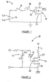
- FIG 1 there is shown a basic diagram of a triggering circuit 10 according to the invention for an insulated gate semiconductor device 12 such as a metal oxide semiconductor field effect transistor (MOSFET).
- MOSFET metal oxide semiconductor field effect transistor
- a power MOSFET is shown and which is available from International Rectifier under the trademark HEXFET number IRF740.
- a 10% to 90% rise time of an output voltage is specified in publicly available user data sheets of the device as being about 27ns and a corresponding fall time is specified as being in the order of 24ns. These times may be too long for some applications of the MOSFET.
- the turn-on delay time is specified at 14ns and the turn-off delay time as 50ns.
- the triggering circuit 10 comprises a charge storage device in the form of a capacitor 14 having first and second terminals 14.1 and 14.2 respectively.
- the first terminal 14.1 is connected in a circuit 17 to a fast switching device 16.
- An optional inductor 18 is connected between the fast switching device 16 and a gate 20 of the MOSFET.
- the drain and source of the MOSFET are shown at 22 and 24 respectively.
- the fast switching device 16 may be any suitable device having a switching speed faster than the data sheet specified turn-on delay time and/or turn-off delay time of the MOSFET, preferably better than 2ns.
- Such devices may include a SIDAC, a break-over diode, a suitably configured bipolar transistor arrangement, or any other suitable fast switching device or circuit.
- the fast switching device is switched on electronically which rapidly transfers sufficient charge from the capacitor 14 to the gate 20 of the MOSFET, to switch the MOSFET on.
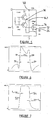
- Time diagrams for the circuit in figure 1 are shown in figures 3 and 4 .
- the diagrams in broken lines indicate normal specified operation of the MOSFET 12.
- diagram 30 in figure 3 shows the gate voltage of the MOSFET during conventional switching on.
- the MOSFET is switched on at 32 and the diagram illustrates a turn-on delay time of about 34ns.
- the associated gate current is shown at 34 in figure 4 .
- the diagrams for the method according to the invention are shown at 36 and 38 in figures 3 and 4 respectively.
- the aforementioned rapid transfer of charge from capacitor 14 through switch 16 and consequent build up of voltage on the gate of the MOSFET are shown.
- the subsequent fall in the gate voltage shown at 42 is attributable to the aforementioned Miller effect.
- the associated current at the gate 20 is shown at 38 in figure 4 . Initially, during the charge transfer stage, the gate current is high and thereafter it drops to a negligible level. It is also believed that with drain currents within the data specification of the MOSFET, switching losses with the switching method and circuit according to the invention are also reduced.
- the value (C) of the capacitor 14, the voltage (V c ) required on the capacitor before switching and hence the breakthrough voltage of the switching device 16, the gate threshold voltage (V t ) of the MOSFET 12 and the gate charge (Q s ) required for complete switching of the MOSFET are related according to the following equation: C Vc Qs / Vt + C > Vt
- FIG 2 a circuit diagram of the triggering circuit 10 is shown wherein the first switching device 16 is a SIDAC.
- a periodic voltage is applied across a capacitor 14, in parallel with a series connection of SIDAC 16 and the gate-source path of a MOSFET 12. Initially, during a first half cycle, the voltage supplied at the input 19 is insufficient to switch the SIDAC 16 on and the capacitor 14 is hence charged up. When the supplied voltage reaches the threshold of the SIDAC 16 it switches on, resulting in a closed circuit from the capacitor 14 to the gate 20 of the MOSFET 12, partially discharging the capacitor 14 and hence charging the gate 20. The result is that a charge will now be shared between the capacitor 14 and the gate 20, so that some voltage, preferably above the gate threshold relative to ground, is applied to the gate.
- the gate voltage may for short intervals be driven approximately three to four times beyond the maximum gate-to-source voltage rating of some MOSFETs 12 without destroying the device.
- the gate voltage of the MOSFET, 12 drops to substantially below the threshold voltage of the MOSFET 12 shortly after the charge dissipates from the gate 20 of the MOSFET 12. As a result, the MOSFET 12 will turn off and the drain current will no longer flow.
- the fast switching means 16 comprises a bipolar transistor arrangement.
- the voltage waveform at 50 is shown in figure 6 .
- the voltage waveform at source 24 is shown in figure 7 . From the latter waveform it can be seen at 52 that the source 24 of the aforementioned MOSFET 12 switches between an "off"-state to an "on”-state through about 400V in a rise time t r of about 4ns, which is substantially quicker than the specified rise time of 27ns. Similarly, and as shown at 54 it switches from the "on"-state to the "off”-state in a fall time t f of about 15ns, which is also substantially shorter than a specified fall time of about 24ns.
- FIG 8 the same triggering circuit 10 is shown for an insulated gate bipolar transistor 60 having a gate 62, a collector 64 and an emitter 66.
- the transistor is an IRG4PC50W device which is being manufactured and sold by International Rectifier.
- the waveform at 68 in figure 8 is shown in figure 9 and the waveform at emitter 66 adjacent load 70 is shown in figure 10 .
- the switching means comprises a low output impedance, high voltage, fast switching driving circuit 116.
- the device 116 must be able to switch between OV and Vd in a first time period shorter than a specified turn-on delay time of the device 12.
- Vd is preferably bigger than 20xVt. Devices of this nature are available on the market.
Description
- This invention relates to a circuit and method for improving the switching speed of insulated gate semiconductor devices such as metal oxide field effect transistors (MOSFET's), more particularly power MOSFET's.
- Capacitance inherent in transistor junctions limits the speed at which a voltage within a circuit can switch. It is also well known that the Miller effect has an influence on the capacitance at the gate of devices of the aforementioned kind.
- Prior art teaches a number of methods of alleviating the Miller effect in high frequency transistor switching circuits, for example by reducing source impedance or reducing feedback capacitance, or both.
- Even with such improvements, an output of a MOSFET such as an IRF740 typically switches through 200 volts in a rise time of approximately 27ns at a peak current of 10 amperes and in a fall time of approximately 24ns. These times may be too long for many applications.
- Accordingly, it is an object of the present invention to provide a triggering circuit and method for improving the rise and/or fall times of insulated gate semiconductor devices with which the applicant believes the aforementioned disadvantages will at least be alleviated.
- According to a first aspect of the present invention there is provided a method according to
claim 1. - The insulated gate semiconductor device may be a metal oxide semiconductor field effect transistor (MOSFET), such as a power MOSFET.
- Alternatively, the insulated gate semiconductor device may be an insulated gate bipolar transistor.
- The charging pulse may raise the gate voltage of the insulated gate semiconductor device three to four times beyond a maximum rating of the semiconductor device.
- The switching means may be connected between the charge storage device and the gate of the semiconductor device.
- Alternatively, the charge storage device may be connected in parallel with the switching means and the insulated gate semiconductor device.
- As a further alternative, the charge storage device may be connected in series with the switching means and the insulated gate semiconductor device.
- The switching means may be a SIDAC.
- Alternatively, the switching means may be selected from a break-over diode, a bipolar transistor, a further insulated gate semiconductor device and a high voltage fast switching device.
- Electronic control means may be provided for the switching means.
- The charge storage device may comprise a capacitor.
- An inductor may be provided between the switching means and the gate.
- Alternatively, an inductor may be connected in series with the switching means.
- The circuit may be integrated on a single chip.
- According to a second aspect of the invention there is provided a circuit according to
claim 16. - The invention will now be described, by way of example only, with reference to the accompanying drawings wherein:
- figure 1
- is a basic circuit diagram of a triggering circuit according to the invention for a MOSFET;
- figure 2
- is a diagram of one embodiment of the circuit comprising a SIDAC as fast switching device;
- figure 3
- includes a diagram in dotted lines of gate voltage against time of normal specified operation of the MOSFET and a diagram in solid lines of operation according to the method of the invention;
- figure 4
- includes a diagram in dotted lines of gate current against time of normal specified operation of the MOSFET and a diagram in solid lines of operation according to the method of the invention;
- figure 5
- is a diagram of another embodiment of the circuit according to the invention;
- figure 6
- is a waveform of voltage against time at a first terminal of a charge storage capacitor in
figure 5 ; - figure 7
- is a waveform of voltage against time at the source of the MOSFET in
figure 5 ; - figure 8
- is a diagram of a triggering circuit for an insulated gate bipolar transistor;
- figure 9
- is a waveform of voltage against time at a first terminal of a charge storage capacitor in the circuit in
figure 8 ; - figure 10
- is a waveform of voltage against time at an emitter of the transistor in
figure 8 ; and - figure 11
- is a basic circuit diagram of yet another embodiment of the triggering circuit.
- In
figure 1 , there is shown a basic diagram of a triggeringcircuit 10 according to the invention for an insulatedgate semiconductor device 12 such as a metal oxide semiconductor field effect transistor (MOSFET). - In the diagram a power MOSFET is shown and which is available from International Rectifier under the trademark HEXFET number IRF740. A 10% to 90% rise time of an output voltage is specified in publicly available user data sheets of the device as being about 27ns and a corresponding fall time is specified as being in the order of 24ns. These times may be too long for some applications of the MOSFET. The turn-on delay time is specified at 14ns and the turn-off delay time as 50ns.
- The triggering
circuit 10 comprises a charge storage device in the form of acapacitor 14 having first and second terminals 14.1 and 14.2 respectively. The first terminal 14.1 is connected in a circuit 17 to afast switching device 16. Anoptional inductor 18 is connected between thefast switching device 16 and agate 20 of the MOSFET. The drain and source of the MOSFET are shown at 22 and 24 respectively. - The
fast switching device 16 may be any suitable device having a switching speed faster than the data sheet specified turn-on delay time and/or turn-off delay time of the MOSFET, preferably better than 2ns. Such devices may include a SIDAC, a break-over diode, a suitably configured bipolar transistor arrangement, or any other suitable fast switching device or circuit. - To switch the MOSFET on, the fast switching device is switched on electronically which rapidly transfers sufficient charge from the
capacitor 14 to thegate 20 of the MOSFET, to switch the MOSFET on. - Time diagrams for the circuit in
figure 1 are shown infigures 3 and 4 . The diagrams in broken lines indicate normal specified operation of theMOSFET 12. Hence, diagram 30 infigure 3 shows the gate voltage of the MOSFET during conventional switching on. The MOSFET is switched on at 32 and the diagram illustrates a turn-on delay time of about 34ns. The associated gate current is shown at 34 infigure 4 . - The diagrams for the method according to the invention are shown at 36 and 38 in
figures 3 and 4 respectively. At 40 infigure 3 , the aforementioned rapid transfer of charge fromcapacitor 14 throughswitch 16 and consequent build up of voltage on the gate of the MOSFET are shown. The subsequent fall in the gate voltage shown at 42 is attributable to the aforementioned Miller effect. What is clear though is that the device switches on at 44, after a mere 4ns. The associated current at thegate 20 is shown at 38 infigure 4 . Initially, during the charge transfer stage, the gate current is high and thereafter it drops to a negligible level. It is also believed that with drain currents within the data specification of the MOSFET, switching losses with the switching method and circuit according to the invention are also reduced. - The value (C) of the
capacitor 14, the voltage (Vc) required on the capacitor before switching and hence the breakthrough voltage of theswitching device 16, the gate threshold voltage (Vt) of theMOSFET 12 and the gate charge (Qs) required for complete switching of the MOSFET are related according to the following equation:
- In
figure 2 a circuit diagram of the triggeringcircuit 10 is shown wherein thefirst switching device 16 is a SIDAC. - A periodic voltage is applied across a
capacitor 14, in parallel with a series connection of SIDAC 16 and the gate-source path of aMOSFET 12. Initially, during a first half cycle, the voltage supplied at the input 19 is insufficient to switch theSIDAC 16 on and thecapacitor 14 is hence charged up. When the supplied voltage reaches the threshold of theSIDAC 16 it switches on, resulting in a closed circuit from thecapacitor 14 to thegate 20 of theMOSFET 12, partially discharging thecapacitor 14 and hence charging thegate 20. The result is that a charge will now be shared between thecapacitor 14 and thegate 20, so that some voltage, preferably above the gate threshold relative to ground, is applied to the gate. - Using this method, the gate voltage may for short intervals be driven approximately three to four times beyond the maximum gate-to-source voltage rating of some
MOSFETs 12 without destroying the device. - Similarly, when during the other half cycle the gate voltage exceeds the reverse threshold of the
SIDAC 16 and current is conducted in the opposite direction, the gate voltage of the MOSFET, 12 drops to substantially below the threshold voltage of theMOSFET 12 shortly after the charge dissipates from thegate 20 of theMOSFET 12. As a result, theMOSFET 12 will turn off and the drain current will no longer flow. - In
figure 5 , an alternative and self-oscillating triggering circuit for theMOSFET 12 is shown. Components thereof corresponding to components of the circuits infigures 1 and 2 are designated utilizing like reference numerals. In this embodiment, the fast switching means 16 comprises a bipolar transistor arrangement. - The voltage waveform at 50 is shown in
figure 6 . The voltage waveform atsource 24 is shown infigure 7 . From the latter waveform it can be seen at 52 that thesource 24 of theaforementioned MOSFET 12 switches between an "off"-state to an "on"-state through about 400V in a rise time tr of about 4ns, which is substantially quicker than the specified rise time of 27ns. Similarly, and as shown at 54 it switches from the "on"-state to the "off"-state in a fall time tf of about 15ns, which is also substantially shorter than a specified fall time of about 24ns. - In
figure 8 , the same triggeringcircuit 10 is shown for an insulated gatebipolar transistor 60 having agate 62, acollector 64 and anemitter 66. The transistor is an IRG4PC50W device which is being manufactured and sold by International Rectifier. The waveform at 68 infigure 8 is shown infigure 9 and the waveform atemitter 66adjacent load 70 is shown infigure 10 . - From the latter waveform it can be seen at 72 that the
emitter 66 switches between an "off"-state and an "on"-state through about 400V in a rise time t, of about 4ns, which is substantially less than a specified rise time of 33ns. - In
figure 11 a further embodiment of the triggering circuit is shown. The switching means comprises a low output impedance, high voltage, fast switching drivingcircuit 116. Thedevice 116 must be able to switch between OV and Vd in a first time period shorter than a specified turn-on delay time of thedevice 12. Vd is preferably bigger than 20xVt. Devices of this nature are available on the market. - It will be appreciated that there are many variations in detail on the triggering circuit and method according to the invention, without departing from the scope of the appended claims.
Claims (16)
- A method of using a circuit to drive an insulated gate semiconductor device (12) comprising as a first terminal a gate (20) and at least second and third terminals (22, 24), the circuit comprising a charge storage device (14) and switching means (16, 116) connected in a series circuit to the gate of the semiconductor device to apply from the charge storage device a charging pulse to the gate of the semiconductor device so as to switch the semiconductor device between one of an on state and an off state and the other of the on state and the off state, characterised in that the switching speed of the switching means is less than 2ns whereby the duration of the charging pulse is such that the charging pulse is complete prior to a change in the current flow between the second and third terminals (22, 24) of the semiconductor device and in that the charging pulse applies a voltage to the gate three to four times beyond the gate maximum voltage rating of the semiconductor device.
- A method according to claim 1, characterised in that the insulated gate semiconductor device (12) is a metal oxide semiconductor field effect transistor.
- A method according to claim 2, characterised in that the metal oxide semiconductor field effect transistor is a power metal oxide semiconductor field effect transistor.
- A method according to claim 1, characterised in that the insulated gate semiconductor device (12) is an insulated gate bipolar transistor.
- A method according to any preceding claim, characterised in that the charging pulse raises the gate voltage of the insulated gate semiconductor device (12) three to four times beyond a maximum rating of the semiconductor device.
- A method according to any preceding claim, characterised in that the switching means (16) is connected between the charge storage device (14) and the gate (20) of the semiconductor device (12).
- A method according to any preceding claim, characterised in that a periodic voltage is applied across a capacitor forming the charge storage device (14), in parallel with a series connection of a SIDAC forming the switching means (16) and the gate-source path of a MOSFET forming the semiconductor device (12).
- A method according to any one of claims 1 to 6, characterised in that the charge storage device (14) is connected in series with the switching means (16, 116) and the insulated gate semiconductor device (12).
- A method according to any preceding claim, characterised in that the switching means (16) is a SIDAC.
- A method according to any one of claims 1 to 8, characterised in that the switching means (16) is selected from a break-over diode, a bipolar transistor, a further insulated gate semiconductor device and a high voltage fast switching device (116).
- A method according to any preceding claim, characterised in that electronic control means is provided for the switching means (16).
- A method according to any preceding claim, characterised in that the charge storage device (14) comprises a capacitor.
- A method according to any preceding claim, characterised in that an inductor (18) is provided between the switching means (16, 116) and the gate (20).
- A method according to any one of claims 1 to 12, characterised in that an inductor (18) is connected in series with the switching means (16, 116).
- A method according to any preceding claim, characterised in that the circuit is integrated on a single chip.
- A circuit for driving an insulated gate semiconductor device (12) comprising as a first terminal a gate (20) and at least second and third terminals (22, 24), the circuit comprising a charge storage device (14) and switching means (16, 116) connected in a series circuit to the gate of the semiconductor device to apply from the charge storage device a charging pulse to the gate of the semiconductor device so as to switch the semiconductor device between one of an on state and an off state and the other of the on state and the off state, characterised in that the switching speed of the switching means is less than 2ns whereby the duration of the charging pulse is such that the charging pulse is complete prior to a change in the current flow between the second and third terminals (22, 24) of the semiconductor device and in that the charging pulse applies a voltage to the gate three to four times beyond the gate maximum voltage rating of the semiconductor device.
Priority Applications (1)
| Application Number | Priority Date | Filing Date | Title |
|---|---|---|---|
| EP16174333.1A EP3096455A1 (en) | 2000-02-23 | 2001-02-23 | Drive circuit and method for mosfet |
Applications Claiming Priority (3)
| Application Number | Priority Date | Filing Date | Title |
|---|---|---|---|
| ZA200000887 | 2000-02-23 | ||
| ZA200000887 | 2000-02-23 | ||
| PCT/ZA2001/000024 WO2001063763A2 (en) | 2000-02-23 | 2001-02-23 | Drive circuit and method for mosfet |
Related Child Applications (1)
| Application Number | Title | Priority Date | Filing Date |
|---|---|---|---|
| EP16174333.1A Division EP3096455A1 (en) | 2000-02-23 | 2001-02-23 | Drive circuit and method for mosfet |
Publications (2)
| Publication Number | Publication Date |
|---|---|
| EP1264402A2 EP1264402A2 (en) | 2002-12-11 |
| EP1264402B1 true EP1264402B1 (en) | 2016-06-15 |
Family
ID=25588635
Family Applications (2)
| Application Number | Title | Priority Date | Filing Date |
|---|---|---|---|
| EP16174333.1A Withdrawn EP3096455A1 (en) | 2000-02-23 | 2001-02-23 | Drive circuit and method for mosfet |
| EP01918992.7A Expired - Lifetime EP1264402B1 (en) | 2000-02-23 | 2001-02-23 | Drive circuit and method for mosfet |
Family Applications Before (1)
| Application Number | Title | Priority Date | Filing Date |
|---|---|---|---|
| EP16174333.1A Withdrawn EP3096455A1 (en) | 2000-02-23 | 2001-02-23 | Drive circuit and method for mosfet |
Country Status (6)
| Country | Link |
|---|---|
| EP (2) | EP3096455A1 (en) |
| JP (1) | JP2003524982A (en) |
| CN (1) | CN1522495A (en) |
| AU (1) | AU2001246004A1 (en) |
| ES (1) | ES2593907T3 (en) |
| WO (1) | WO2001063763A2 (en) |
Families Citing this family (4)
| Publication number | Priority date | Publication date | Assignee | Title |
|---|---|---|---|---|
| DE10306809A1 (en) | 2003-02-18 | 2004-09-02 | Siemens Ag | Operation of a half-bridge, in particular a field-effect transistor half-bridge |
| JP4755455B2 (en) * | 2005-07-07 | 2011-08-24 | ローム株式会社 | Control circuit for controlling on / off of power transistor, switching regulator using the same, and electronic device |
| JP4804142B2 (en) * | 2005-12-21 | 2011-11-02 | 東洋電機製造株式会社 | High-speed gate drive circuit |
| WO2007135584A1 (en) * | 2006-05-18 | 2007-11-29 | North-West University | Ignition system |
Citations (2)
| Publication number | Priority date | Publication date | Assignee | Title |
|---|---|---|---|---|
| JPH1197995A (en) * | 1997-09-19 | 1999-04-09 | Origin Electric Co Ltd | Method for driving electric field control type semiconductor element and circuit therefor |
| WO2000050338A1 (en) * | 1999-02-24 | 2000-08-31 | Potchefstroom University For Christian Higher Education | Method and apparatus for producing ozone |
Family Cites Families (6)
| Publication number | Priority date | Publication date | Assignee | Title |
|---|---|---|---|---|
| US4912335A (en) * | 1988-03-07 | 1990-03-27 | Dionics Inc. | Means for rapid charging and dynamic discharging of a capacitively charged electrical device |
| JP2776517B2 (en) * | 1988-09-26 | 1998-07-16 | 日本電気株式会社 | Semiconductor device |
| JPH03286619A (en) * | 1990-04-02 | 1991-12-17 | Mitsubishi Electric Corp | Gate driver circuit for isolation gate type semiconductor device and flash controller using same circuit |
| JPH05122035A (en) * | 1991-05-10 | 1993-05-18 | Fuji Electric Co Ltd | Semiconductor device with built-in driving power source |
| US5504449A (en) * | 1992-04-09 | 1996-04-02 | Harris Corporation | Power driver circuit |
| JPH05335911A (en) * | 1992-05-28 | 1993-12-17 | Hitachi Ltd | Drive circuit |
-
2001
- 2001-02-23 AU AU2001246004A patent/AU2001246004A1/en not_active Abandoned
- 2001-02-23 CN CNA01805515XA patent/CN1522495A/en active Pending
- 2001-02-23 EP EP16174333.1A patent/EP3096455A1/en not_active Withdrawn
- 2001-02-23 EP EP01918992.7A patent/EP1264402B1/en not_active Expired - Lifetime
- 2001-02-23 WO PCT/ZA2001/000024 patent/WO2001063763A2/en active Application Filing
- 2001-02-23 JP JP2001562839A patent/JP2003524982A/en active Pending
- 2001-02-23 ES ES01918992.7T patent/ES2593907T3/en not_active Expired - Lifetime
Patent Citations (2)
| Publication number | Priority date | Publication date | Assignee | Title |
|---|---|---|---|---|
| JPH1197995A (en) * | 1997-09-19 | 1999-04-09 | Origin Electric Co Ltd | Method for driving electric field control type semiconductor element and circuit therefor |
| WO2000050338A1 (en) * | 1999-02-24 | 2000-08-31 | Potchefstroom University For Christian Higher Education | Method and apparatus for producing ozone |
Non-Patent Citations (1)
| Title |
|---|
| MCGINTY, J.: "Application note 24 - Designing with Low-Side MOSFET Drivers"", March 1998 (1998-03-01), MICREL INC, SAN JOSE, CA, US, pages 1 - 4 * |
Also Published As
| Publication number | Publication date |
|---|---|
| JP2003524982A (en) | 2003-08-19 |
| CN1522495A (en) | 2004-08-18 |
| EP3096455A1 (en) | 2016-11-23 |
| WO2001063763A3 (en) | 2002-06-13 |
| EP1264402A2 (en) | 2002-12-11 |
| ES2593907T3 (en) | 2016-12-14 |
| WO2001063763A2 (en) | 2001-08-30 |
| AU2001246004A1 (en) | 2001-09-03 |
Similar Documents
| Publication | Publication Date | Title |
|---|---|---|
| JP4804142B2 (en) | High-speed gate drive circuit | |
| US6650169B2 (en) | Gate driver apparatus having an energy recovering circuit | |
| US8729871B2 (en) | Circuit and method for controlling the power supply of a consumer with current pulses having steep flanks | |
| US4459498A (en) | Switch with series-connected MOS-FETs | |
| CN101325364B (en) | Drive circuit for voltage driven electronic element | |
| CN1630929A (en) | A low cost half bridge driver integrated circuit | |
| JPH054849B2 (en) | ||
| JPH06130914A (en) | Plasma display driving device | |
| EP0130273A2 (en) | FET driver circuit | |
| JP3116886B2 (en) | Piezo drive circuit | |
| JP2008182381A (en) | High-speed gate drive circuit | |
| KR840004835A (en) | Integrated Semiconductor Circuits | |
| JPH05505091A (en) | DC power converter with current limiting circuit | |
| US5057721A (en) | Level shift circuit for controlling a driving circuit | |
| US6870405B2 (en) | Method for driving an insulated gate semiconductor device using a short duration pulse | |
| EP1264402B1 (en) | Drive circuit and method for mosfet | |
| US5276357A (en) | High efficiency quasi-square wave drive circuit for switching power amplifiers | |
| US6917227B1 (en) | Efficient gate driver for power device | |
| EP0531941B1 (en) | Method and driver for power field-effect switches with refreshed power supply providing stable on/off switching | |
| US4106088A (en) | Current drive circuits | |
| EP1069683B1 (en) | Gate driving circuit for power semiconductor switch | |
| JP2004229445A (en) | Inverter device | |
| JPS5752230A (en) | Driving system of semiconductor | |
| WO1997043832A1 (en) | Insulated gate bipolar transistor control | |
| JPS601781B2 (en) | two-way switch |
Legal Events
| Date | Code | Title | Description |
|---|---|---|---|
| PUAI | Public reference made under article 153(3) epc to a published international application that has entered the european phase |
Free format text: ORIGINAL CODE: 0009012 |
|
| 17P | Request for examination filed |
Effective date: 20020923 |
|
| AK | Designated contracting states |
Kind code of ref document: A2 Designated state(s): AT BE CH CY DE DK ES FI FR GB GR IE IT LI LU MC NL PT SE TR |
|
| AX | Request for extension of the european patent |
Free format text: AL;LT;LV;MK;RO;SI |
|
| RAP1 | Party data changed (applicant data changed or rights of an application transferred) |
Owner name: NORTH-WEST UNIVERSITY |
|
| 17Q | First examination report despatched |
Effective date: 20090526 |
|
| GRAP | Despatch of communication of intention to grant a patent |
Free format text: ORIGINAL CODE: EPIDOSNIGR1 |
|
| RIC1 | Information provided on ipc code assigned before grant |
Ipc: C01B 13/11 20060101ALN20151216BHEP Ipc: H03K 17/00 20060101AFI20151216BHEP Ipc: H03K 17/567 20060101ALI20151216BHEP Ipc: H03K 17/687 20060101ALI20151216BHEP Ipc: H03K 17/0412 20060101ALI20151216BHEP |
|
| INTG | Intention to grant announced |
Effective date: 20160115 |
|
| GRAS | Grant fee paid |
Free format text: ORIGINAL CODE: EPIDOSNIGR3 |
|
| GRAA | (expected) grant |
Free format text: ORIGINAL CODE: 0009210 |
|
| AK | Designated contracting states |
Kind code of ref document: B1 Designated state(s): AT BE CH CY DE DK ES FI FR GB GR IE IT LI LU MC NL PT SE TR |
|
| REG | Reference to a national code |
Ref country code: CH Ref legal event code: EP Ref country code: GB Ref legal event code: FG4D |
|
| REG | Reference to a national code |
Ref country code: IE Ref legal event code: FG4D |
|
| REG | Reference to a national code |
Ref country code: AT Ref legal event code: REF Ref document number: 806961 Country of ref document: AT Kind code of ref document: T Effective date: 20160715 |
|
| REG | Reference to a national code |
Ref country code: DE Ref legal event code: R096 Ref document number: 60149987 Country of ref document: DE |
|
| REG | Reference to a national code |
Ref country code: SE Ref legal event code: TRGR |
|
| REG | Reference to a national code |
Ref country code: NL Ref legal event code: MP Effective date: 20160615 |
|
| PG25 | Lapsed in a contracting state [announced via postgrant information from national office to epo] |
Ref country code: FI Free format text: LAPSE BECAUSE OF FAILURE TO SUBMIT A TRANSLATION OF THE DESCRIPTION OR TO PAY THE FEE WITHIN THE PRESCRIBED TIME-LIMIT Effective date: 20160615 |
|
| PG25 | Lapsed in a contracting state [announced via postgrant information from national office to epo] |
Ref country code: GR Free format text: LAPSE BECAUSE OF FAILURE TO SUBMIT A TRANSLATION OF THE DESCRIPTION OR TO PAY THE FEE WITHIN THE PRESCRIBED TIME-LIMIT Effective date: 20160916 Ref country code: NL Free format text: LAPSE BECAUSE OF FAILURE TO SUBMIT A TRANSLATION OF THE DESCRIPTION OR TO PAY THE FEE WITHIN THE PRESCRIBED TIME-LIMIT Effective date: 20160615 |
|
| REG | Reference to a national code |
Ref country code: ES Ref legal event code: FG2A Ref document number: 2593907 Country of ref document: ES Kind code of ref document: T3 Effective date: 20161214 |
|
| REG | Reference to a national code |
Ref country code: FR Ref legal event code: PLFP Year of fee payment: 17 |
|
| PG25 | Lapsed in a contracting state [announced via postgrant information from national office to epo] |
Ref country code: BE Free format text: LAPSE BECAUSE OF FAILURE TO SUBMIT A TRANSLATION OF THE DESCRIPTION OR TO PAY THE FEE WITHIN THE PRESCRIBED TIME-LIMIT Effective date: 20160615 Ref country code: PT Free format text: LAPSE BECAUSE OF FAILURE TO SUBMIT A TRANSLATION OF THE DESCRIPTION OR TO PAY THE FEE WITHIN THE PRESCRIBED TIME-LIMIT Effective date: 20161017 |
|
| REG | Reference to a national code |
Ref country code: DE Ref legal event code: R097 Ref document number: 60149987 Country of ref document: DE |
|
| PLBE | No opposition filed within time limit |
Free format text: ORIGINAL CODE: 0009261 |
|
| STAA | Information on the status of an ep patent application or granted ep patent |
Free format text: STATUS: NO OPPOSITION FILED WITHIN TIME LIMIT |
|
| 26N | No opposition filed |
Effective date: 20170316 |
|
| PG25 | Lapsed in a contracting state [announced via postgrant information from national office to epo] |
Ref country code: DK Free format text: LAPSE BECAUSE OF FAILURE TO SUBMIT A TRANSLATION OF THE DESCRIPTION OR TO PAY THE FEE WITHIN THE PRESCRIBED TIME-LIMIT Effective date: 20160615 |
|
| REG | Reference to a national code |
Ref country code: DE Ref legal event code: R082 Ref document number: 60149987 Country of ref document: DE Representative=s name: SCHMITT-NILSON SCHRAUD WAIBEL WOHLFROM PATENTA, DE |
|
| PG25 | Lapsed in a contracting state [announced via postgrant information from national office to epo] |
Ref country code: MC Free format text: LAPSE BECAUSE OF FAILURE TO SUBMIT A TRANSLATION OF THE DESCRIPTION OR TO PAY THE FEE WITHIN THE PRESCRIBED TIME-LIMIT Effective date: 20160615 |
|
| REG | Reference to a national code |
Ref country code: CH Ref legal event code: PL |
|
| PG25 | Lapsed in a contracting state [announced via postgrant information from national office to epo] |
Ref country code: LI Free format text: LAPSE BECAUSE OF NON-PAYMENT OF DUE FEES Effective date: 20170228 Ref country code: CH Free format text: LAPSE BECAUSE OF NON-PAYMENT OF DUE FEES Effective date: 20170228 |
|
| REG | Reference to a national code |
Ref country code: IE Ref legal event code: MM4A |
|
| PG25 | Lapsed in a contracting state [announced via postgrant information from national office to epo] |
Ref country code: LU Free format text: LAPSE BECAUSE OF NON-PAYMENT OF DUE FEES Effective date: 20170223 |
|
| REG | Reference to a national code |
Ref country code: FR Ref legal event code: PLFP Year of fee payment: 18 |
|
| PG25 | Lapsed in a contracting state [announced via postgrant information from national office to epo] |
Ref country code: IE Free format text: LAPSE BECAUSE OF NON-PAYMENT OF DUE FEES Effective date: 20170223 |
|
| PGFP | Annual fee paid to national office [announced via postgrant information from national office to epo] |
Ref country code: IT Payment date: 20190225 Year of fee payment: 19 Ref country code: DE Payment date: 20190219 Year of fee payment: 19 Ref country code: ES Payment date: 20190320 Year of fee payment: 19 Ref country code: GB Payment date: 20190218 Year of fee payment: 19 |
|
| PGFP | Annual fee paid to national office [announced via postgrant information from national office to epo] |
Ref country code: FR Payment date: 20190219 Year of fee payment: 19 Ref country code: AT Payment date: 20190219 Year of fee payment: 19 Ref country code: SE Payment date: 20190218 Year of fee payment: 19 |
|
| PG25 | Lapsed in a contracting state [announced via postgrant information from national office to epo] |
Ref country code: CY Free format text: LAPSE BECAUSE OF NON-PAYMENT OF DUE FEES Effective date: 20160615 |
|
| PG25 | Lapsed in a contracting state [announced via postgrant information from national office to epo] |
Ref country code: TR Free format text: LAPSE BECAUSE OF FAILURE TO SUBMIT A TRANSLATION OF THE DESCRIPTION OR TO PAY THE FEE WITHIN THE PRESCRIBED TIME-LIMIT Effective date: 20160615 |
|
| REG | Reference to a national code |
Ref country code: AT Ref legal event code: UEP Ref document number: 806961 Country of ref document: AT Kind code of ref document: T Effective date: 20160615 |
|
| REG | Reference to a national code |
Ref country code: DE Ref legal event code: R119 Ref document number: 60149987 Country of ref document: DE |
|
| REG | Reference to a national code |
Ref country code: SE Ref legal event code: EUG |
|
| REG | Reference to a national code |
Ref country code: AT Ref legal event code: MM01 Ref document number: 806961 Country of ref document: AT Kind code of ref document: T Effective date: 20200223 |
|
| GBPC | Gb: european patent ceased through non-payment of renewal fee |
Effective date: 20200223 |
|
| PG25 | Lapsed in a contracting state [announced via postgrant information from national office to epo] |
Ref country code: SE Free format text: LAPSE BECAUSE OF NON-PAYMENT OF DUE FEES Effective date: 20200224 |
|
| PG25 | Lapsed in a contracting state [announced via postgrant information from national office to epo] |
Ref country code: AT Free format text: LAPSE BECAUSE OF NON-PAYMENT OF DUE FEES Effective date: 20200223 |
|
| PG25 | Lapsed in a contracting state [announced via postgrant information from national office to epo] |
Ref country code: DE Free format text: LAPSE BECAUSE OF NON-PAYMENT OF DUE FEES Effective date: 20200901 Ref country code: GB Free format text: LAPSE BECAUSE OF NON-PAYMENT OF DUE FEES Effective date: 20200223 Ref country code: FR Free format text: LAPSE BECAUSE OF NON-PAYMENT OF DUE FEES Effective date: 20200229 |
|
| REG | Reference to a national code |
Ref country code: ES Ref legal event code: FD2A Effective date: 20210708 |
|
| PG25 | Lapsed in a contracting state [announced via postgrant information from national office to epo] |
Ref country code: IT Free format text: LAPSE BECAUSE OF NON-PAYMENT OF DUE FEES Effective date: 20200223 |
|
| PG25 | Lapsed in a contracting state [announced via postgrant information from national office to epo] |
Ref country code: ES Free format text: LAPSE BECAUSE OF NON-PAYMENT OF DUE FEES Effective date: 20200224 |