EP1264169B1 - Improvement of spectral and/or spatial resolution in a laser scanning microscope - Google Patents
Improvement of spectral and/or spatial resolution in a laser scanning microscope Download PDFInfo
- Publication number
- EP1264169B1 EP1264169B1 EP01958054A EP01958054A EP1264169B1 EP 1264169 B1 EP1264169 B1 EP 1264169B1 EP 01958054 A EP01958054 A EP 01958054A EP 01958054 A EP01958054 A EP 01958054A EP 1264169 B1 EP1264169 B1 EP 1264169B1
- Authority
- EP
- European Patent Office
- Prior art keywords
- detector
- fluorescence
- laser scanning
- displacement
- scanning microscope
- Prior art date
- Legal status (The legal status is an assumption and is not a legal conclusion. Google has not performed a legal analysis and makes no representation as to the accuracy of the status listed.)
- Expired - Lifetime
Links
- 230000003595 spectral effect Effects 0.000 title claims description 34
- 238000001514 detection method Methods 0.000 claims abstract description 60
- 238000000034 method Methods 0.000 claims abstract description 45
- 230000005855 radiation Effects 0.000 claims abstract description 21
- 238000006073 displacement reaction Methods 0.000 claims abstract description 20
- 239000000975 dye Substances 0.000 claims description 46
- 238000010521 absorption reaction Methods 0.000 claims description 25
- 238000003384 imaging method Methods 0.000 claims description 18
- 238000000295 emission spectrum Methods 0.000 claims description 10
- 238000004422 calculation algorithm Methods 0.000 claims description 6
- 238000005259 measurement Methods 0.000 claims description 6
- 238000005286 illumination Methods 0.000 claims description 5
- 230000000694 effects Effects 0.000 claims description 4
- 230000010354 integration Effects 0.000 claims description 4
- 238000000386 microscopy Methods 0.000 claims description 4
- 230000001419 dependent effect Effects 0.000 claims description 3
- 238000004364 calculation method Methods 0.000 claims description 2
- 238000006243 chemical reaction Methods 0.000 claims description 2
- 102000004190 Enzymes Human genes 0.000 claims 2
- 108090000790 Enzymes Proteins 0.000 claims 2
- 239000013543 active substance Substances 0.000 claims 2
- 238000013513 substance screening Methods 0.000 claims 2
- 238000011144 upstream manufacturing Methods 0.000 claims 2
- 238000000862 absorption spectrum Methods 0.000 claims 1
- 238000002073 fluorescence micrograph Methods 0.000 claims 1
- 238000004020 luminiscence type Methods 0.000 claims 1
- 230000003287 optical effect Effects 0.000 abstract description 12
- 230000005284 excitation Effects 0.000 description 24
- 239000000523 sample Substances 0.000 description 16
- 239000011159 matrix material Substances 0.000 description 11
- 238000010276 construction Methods 0.000 description 9
- 238000002360 preparation method Methods 0.000 description 7
- 238000001228 spectrum Methods 0.000 description 7
- 238000010586 diagram Methods 0.000 description 6
- 238000002189 fluorescence spectrum Methods 0.000 description 6
- 238000000926 separation method Methods 0.000 description 4
- 230000008859 change Effects 0.000 description 3
- 238000000799 fluorescence microscopy Methods 0.000 description 3
- 238000011835 investigation Methods 0.000 description 3
- 210000001747 pupil Anatomy 0.000 description 3
- XKRFYHLGVUSROY-UHFFFAOYSA-N Argon Chemical compound [Ar] XKRFYHLGVUSROY-UHFFFAOYSA-N 0.000 description 2
- 230000008901 benefit Effects 0.000 description 2
- 239000003814 drug Substances 0.000 description 2
- 229940079593 drug Drugs 0.000 description 2
- 238000001917 fluorescence detection Methods 0.000 description 2
- 239000007850 fluorescent dye Substances 0.000 description 2
- 230000005283 ground state Effects 0.000 description 2
- 238000002372 labelling Methods 0.000 description 2
- 238000000399 optical microscopy Methods 0.000 description 2
- 230000008569 process Effects 0.000 description 2
- 238000012216 screening Methods 0.000 description 2
- 230000035945 sensitivity Effects 0.000 description 2
- 238000004611 spectroscopical analysis Methods 0.000 description 2
- 230000007704 transition Effects 0.000 description 2
- 206010067482 No adverse event Diseases 0.000 description 1
- 230000006978 adaptation Effects 0.000 description 1
- 229910052786 argon Inorganic materials 0.000 description 1
- WZSUOQDIYKMPMT-UHFFFAOYSA-N argon krypton Chemical compound [Ar].[Kr] WZSUOQDIYKMPMT-UHFFFAOYSA-N 0.000 description 1
- 239000012472 biological sample Substances 0.000 description 1
- 230000005540 biological transmission Effects 0.000 description 1
- 238000004624 confocal microscopy Methods 0.000 description 1
- 230000008878 coupling Effects 0.000 description 1
- 238000010168 coupling process Methods 0.000 description 1
- 238000005859 coupling reaction Methods 0.000 description 1
- 239000013078 crystal Substances 0.000 description 1
- 238000011161 development Methods 0.000 description 1
- 230000018109 developmental process Effects 0.000 description 1
- 238000009792 diffusion process Methods 0.000 description 1
- 238000011156 evaluation Methods 0.000 description 1
- 230000005281 excited state Effects 0.000 description 1
- 239000000835 fiber Substances 0.000 description 1
- 102000034287 fluorescent proteins Human genes 0.000 description 1
- 108091006047 fluorescent proteins Proteins 0.000 description 1
- 231100000252 nontoxic Toxicity 0.000 description 1
- 238000005070 sampling Methods 0.000 description 1
- 238000002500 scanning fluorescence correlation spectroscopy Methods 0.000 description 1
- 238000001758 scanning near-field microscopy Methods 0.000 description 1
- 238000004621 scanning probe microscopy Methods 0.000 description 1
- 230000000638 stimulation Effects 0.000 description 1
Images


Classifications
-
- G—PHYSICS
- G01—MEASURING; TESTING
- G01N—INVESTIGATING OR ANALYSING MATERIALS BY DETERMINING THEIR CHEMICAL OR PHYSICAL PROPERTIES
- G01N21/00—Investigating or analysing materials by the use of optical means, i.e. using sub-millimetre waves, infrared, visible or ultraviolet light
- G01N21/17—Systems in which incident light is modified in accordance with the properties of the material investigated
- G01N21/25—Colour; Spectral properties, i.e. comparison of effect of material on the light at two or more different wavelengths or wavelength bands
- G01N21/27—Colour; Spectral properties, i.e. comparison of effect of material on the light at two or more different wavelengths or wavelength bands using photo-electric detection ; circuits for computing concentration
-
- G—PHYSICS
- G01—MEASURING; TESTING
- G01N—INVESTIGATING OR ANALYSING MATERIALS BY DETERMINING THEIR CHEMICAL OR PHYSICAL PROPERTIES
- G01N21/00—Investigating or analysing materials by the use of optical means, i.e. using sub-millimetre waves, infrared, visible or ultraviolet light
- G01N21/17—Systems in which incident light is modified in accordance with the properties of the material investigated
- G01N21/47—Scattering, i.e. diffuse reflection
- G01N21/4738—Diffuse reflection, e.g. also for testing fluids, fibrous materials
-
- G—PHYSICS
- G01—MEASURING; TESTING
- G01N—INVESTIGATING OR ANALYSING MATERIALS BY DETERMINING THEIR CHEMICAL OR PHYSICAL PROPERTIES
- G01N21/00—Investigating or analysing materials by the use of optical means, i.e. using sub-millimetre waves, infrared, visible or ultraviolet light
- G01N21/62—Systems in which the material investigated is excited whereby it emits light or causes a change in wavelength of the incident light
- G01N21/63—Systems in which the material investigated is excited whereby it emits light or causes a change in wavelength of the incident light optically excited
- G01N21/64—Fluorescence; Phosphorescence
- G01N21/645—Specially adapted constructive features of fluorimeters
-
- G—PHYSICS
- G01—MEASURING; TESTING
- G01Q—SCANNING-PROBE TECHNIQUES OR APPARATUS; APPLICATIONS OF SCANNING-PROBE TECHNIQUES, e.g. SCANNING PROBE MICROSCOPY [SPM]
- G01Q60/00—Particular types of SPM [Scanning Probe Microscopy] or microscopes; Essential components thereof
- G01Q60/18—SNOM [Scanning Near-Field Optical Microscopy] or apparatus therefor, e.g. SNOM probes
- G01Q60/20—Fluorescence
-
- G—PHYSICS
- G02—OPTICS
- G02B—OPTICAL ELEMENTS, SYSTEMS OR APPARATUS
- G02B21/00—Microscopes
- G02B21/0004—Microscopes specially adapted for specific applications
-
- G—PHYSICS
- G02—OPTICS
- G02B—OPTICAL ELEMENTS, SYSTEMS OR APPARATUS
- G02B21/00—Microscopes
- G02B21/0004—Microscopes specially adapted for specific applications
- G02B21/002—Scanning microscopes
-
- G—PHYSICS
- G02—OPTICS
- G02B—OPTICAL ELEMENTS, SYSTEMS OR APPARATUS
- G02B21/00—Microscopes
- G02B21/16—Microscopes adapted for ultraviolet illumination ; Fluorescence microscopes
-
- G—PHYSICS
- G01—MEASURING; TESTING
- G01N—INVESTIGATING OR ANALYSING MATERIALS BY DETERMINING THEIR CHEMICAL OR PHYSICAL PROPERTIES
- G01N21/00—Investigating or analysing materials by the use of optical means, i.e. using sub-millimetre waves, infrared, visible or ultraviolet light
- G01N21/62—Systems in which the material investigated is excited whereby it emits light or causes a change in wavelength of the incident light
- G01N21/63—Systems in which the material investigated is excited whereby it emits light or causes a change in wavelength of the incident light optically excited
- G01N21/64—Fluorescence; Phosphorescence
- G01N2021/6417—Spectrofluorimetric devices
Definitions
- the invention relates to a method and an arrangement in fluorescence microscopy, in particular laser scanning microscopy, fluorescence correlation spectroscopy and scanning near field microscopy, for the examination of predominantly biological samples, preparations and associated components. Included are fluorescence detection based methods for the screening of drugs (High Throughput Sceening). The transition from the detection of a few broad spectral dye bands to the simultaneous acquisition of complete spectra opens up new possibilities in the identification, separation and assignment of mostly analytical or functional sample properties to spatial substructures or dynamic processes. Simultaneous investigations of samples with multiple fluorophores are thus possible with overlapping fluorescence spectra even in spatial structures of thick samples. The arrangement increases the spectral and spatial resolution of the detection unit.
- the irradiated photons of a certain energy excite the dye molecules by the absorption of a photon from the ground state in an excited state.
- This excitation is usually referred to as single-photon absorption ( Fig. 1a ).
- the dye molecules excited in this way can return to the ground state in various ways.
- fluorescence microscopy the transition under emission of a fluorescence photon is most important.
- the wavelength of the emitted photon is due to the Stokes shift compared to Stimulation radiation generally red shifted, so has a larger wavelength. The Stokes shift allows the separation of fluorescence radiation from the excitation radiation.
- the fluorescent light is split off from the excitation radiation with suitable dichroic beam splitters in combination with block filters and observed separately.
- suitable dichroic beam splitters in combination with block filters and observed separately.
- LSM confocal laser scanning microscope
- An LSM is essentially divided into 4 modules: light source, scan module, detection unit and microscope. These modules are described in more detail below. It is additionally on DE19702753A1 directed.
- lasers with different wavelengths are used in one LSM.
- the choice of the excitation wavelength depends on the absorption properties of the dyes to be investigated.
- the excitation radiation is generated in the light source module.
- Various lasers are used here (argon, argon krypton, TiSa laser).
- the selection of the wavelengths and the adjustment of the intensity of the required excitation wavelength e.g. through the use of an acousto-optic crystal.
- the laser radiation passes through a fiber or a suitable mirror arrangement in the scan module.
- the laser radiation generated in the light source is focused by means of the lens (2) diffraction-limited on the scanner, the scanning optics and the tube lens in the preparation.
- the focus scans the sample punctiformly in the x-y direction.
- the pixel dwell times when scanning across the sample are usually in the range of less than one microsecond to several seconds.
- the light which is emitted from the focal plane (specimen) and from the planes above and below passes through the scanners to a dichroic beam splitter (MDB).
- MDB dichroic beam splitter
- the fluorescent light is focused on a diaphragm (confocal aperture / pinhole), which is located exactly in a plane conjugate to the focal plane.
- EF dichroic block filter
- the fluorescent light is measured by means of a point detector (PMT).
- the excitation of the dye fluorescence occurs in a small volume in which the excitation intensity is particularly high. This area is only marginally larger than the detected area using a confocal array.
- the use of a confocal aperture can thus be dispensed with and the detection can take place directly after the objective (non-descanned detection).
- a descanned detection also takes place, but this time the pupil of the objective is imaged into the detection unit (nonconfocally descanned detection).
- the LSM is therefore suitable for the examination of thick specimens.
- the excitation wavelengths are determined by the dye used with its specific absorption properties. Dichroic filters tuned to the emission characteristics of the dye ensure that only the fluorescent light emitted by the particular dye is measured by the point detector.
- the fluorescent light is spectrally split by means of a prism.
- the method differs from the arrangement with dichroic filters described above only in that the filter used is adjustable in its characteristics.
- the emission band of a dye is preferably recorded per point detector.
- a fast local measurement of the emission spectrum is only partially possible with both arrangements, since the adjustment of the emission range is based on mechanical movements of the dichroic filter or diaphragms and thus the maximum spectral resolution is limited to a few 5 nm.
- a high spectral resolution is required when the emission spectra are as in Fig. 3b overlaid.
- Fig. 3b shows such behavior of two naturally occurring dyes CFP and GFP. These dyes are particularly suitable for the study of live preparations as they exert no toxic effects on the samples to be examined.
- the mostly weak fluorescence signal of the sample is distributed over a large number of individual channels in the spectrometer (usually 512 or 1024 individual channels) or a narrow fluorescence band corresponding to the spectral resolution is detected. Therefore, the signal per single channel is extremely low and may no longer be detectable.
- DE-A-4327944 describes a two-dimensional image detector with a mask slider for a mask in front of a matrix sensor.
- US6088097 describes a point-scanning LSM with spetral splitting by a dispersive element in the detection beam path.
- DE4017317A describes a spectrometer with moving to a spectrum line detector.
- EP0320530 describes a spectrometer with a displaceable to a detector spectrum.
- a disadvantage of the methods according to the prior art is that the line detector usually has to be read out sequentially, which may result in increased readout noise at fast readout rates.
- the object of the invention are therefore new methods for the efficient and spectrally and spatially high-resolution detection of fluorescent dyes. These methods should be able to be used in imaging as well as in analytical microscopy systems.
- the microscope systems are imaging systems such as laser scanning microscopes for the three-dimensional investigation of biological specimens with an optical spatial resolution up to 200 nm, scanning near-field microscopes for the high-resolution examination of surfaces with a resolution of up to 10 nm.
- Fluorescence correlation microscopes for the quantitative determination of molecular concentrations and for the measurement of molecule diffusions. Also included are fluorescence detection based methods for screening dyes. In all the above-mentioned systems, fluorescent dyes are used for the specific labeling of the preparations. The above object is achieved by a method and an arrangement according to the independent patent claims.
- Background of the method according to the invention is a spectrally split detection of fluorescence.
- the emission light in the scanning module or in the microscope is split off from the excitation light by means of an element for separating the excitation radiation from the detected radiation such as the main color splitter (MDB) or an AOTF according to 7346DE or according to 7323DE.
- MDB main color splitter
- AOTF AOTF
- 7346DE 7346DE
- 7323DE AOTF
- a block diagram of the following detector unit is in Fig. 4 shown.
- the light L of the sample is focused by means of an imaging optic PO upon confocal detection through a pinhole PH, thereby suppressing out-of-focus fluorescence.
- a Vietnamesedescannte detection eliminates the aperture.
- the light is now decomposed into its spectral components by means of a angle-dispersive element DI.
- Suitable angle-dispersive elements are prisms, gratings and, for example, acousto-optical elements.
- the light split by the dispersive element into its spectral components is subsequently imaged onto a line detector DE.
- This line detector DE thus measures the emission signal S as a function of the wavelength and converts this into electrical signals.
- the position of the fluorescence spectrum relative to the line detector can be defined by a distance dl by displacement of the PMT in FIG Fig. 5 or by pivoting a grating or mirror by a rotation angle phi ( Fig. 5 and more) are moved.
- the detection unit can be preceded by a line filter for suppressing the excitation wavelengths.
- FIG. 4 A possible embodiment of the optical beam path of in Fig. 4
- the detector unit shown in the block diagram is in Fig. 5 shown.
- Construction essentially describes a Cerny Turner construction.
- the light L of the sample is focused with the pinhol optic PO through the confocal aperture PH.
- this aperture can be omitted.
- the first imaging mirror M2 collimates the fluorescent light.
- the light strikes a line grid G, for example a grid with a line number of 651 lines per mm.
- the grid diffracts the light according to its wavelength in different directions.
- the second imaging mirror M1 focuses the individual spectrally split wavelength components onto the corresponding channels of the line detector DE. Particularly advantageous is the use of a line secondary photomultiplier from Hamamatsu H7260.
- the detector has 32 channels and high sensitivity.
- the free spectral range of the embodiment described above is about 350 nm.
- the free spectral range is uniformly distributed in this arrangement to the 32 channels of the line detector, resulting in an optical resolution of about 10 nm.
- this arrangement is only partially suitable for spectroscopy.
- their use in an imaging system is advantageous because the signal per detection channel is still relatively large due to the relatively wide detected spectral band.
- a shift of the fluorescence spectrum can be effected by a rotation, for example, of the grating, of M1, of M2, by the angle phi and / or by a shift of the line receiver in the direction of the wavelength splitting by dl (see FIG. This corresponds to an advantageous embodiment of the o.g. Wavelength scanner WS.
- Another possible embodiment may involve the use of a matrix detector (eg, a CCD matrix).
- a matrix detector eg, a CCD matrix
- a splitting in the plane of the drawing into different wavelength components is carried out.
- a complete line (or column) of the scanned image is displayed.
- This embodiment is particularly advantageous in the construction of a line scanner.
- the basic structure essentially corresponds to that of an LSM Illustration 2 , However, instead of a point focus, a line is shown as dashed lines, for example being imaged by a cylindrical lens ZL in the focus, and the sample to be examined is scanned only in one direction.
- Non-descanned detection especially when using multiphoton absorption, can also be achieved with this arrangement as in Fig.2 shown, done.
- the slit can be omitted in Mehrphotonenabsorption.
- FIG. 6 A block diagram of the following detector unit is in Fig. 6 shown.
- the light of the sample is focused by means of an imaging optic PO in confocal detection through a slit PH 1, whereby fluorescence that originated outside the focus is suppressed.
- a Caesardescannte detection eliminates the aperture.
- the light can now also with the help of a in Fig. 7 represented mirror SP, which is in a to the scanning mirrors x / y optically conjugate plane (pupil of the optical illumination arrangement), are imaged on the line detector DE.
- the position of the fluorescence line relative to the line detector can be defined by dl shifted (position scanner WS).
- This line detector DE thus measures the emission signal as a function of the position in which the excitation took place in the sample and converts this into electrical signals.
- the detection unit it is advantageous for the detection unit to be preceded by a line filter (not shown) for suppressing the excitation wavelengths.
- a splitting of Fluorescence signals of various dyes with corresponding dichroic filters according to the prior art and separate detection of the fluorescence signals with different detection means part of this invention.
- FIG. 7 A possible embodiment of the optical beam path of in Fig. 6
- the detector unit shown in the block diagram is in Fig. 7 shown.
- the light L of the sample is focused with the pinhol optic PO through the confocal slit PHS.
- this aperture can be omitted.
- the first imaging mirror M2 collimates the fluorescent light.
- the light hits another level mirror SP.
- the mirror SP is located in a pupil of the optical illumination device and is rotatably mounted.
- the second imaging mirror M1 focuses the scan line on the corresponding channels of the line detector DE. Particularly advantageous is the use of a line secondary photomultiplier from Hamamatsu H7260.
- the detector has 32 channels and high sensitivity. Furthermore, the signal per detection channel is still relatively large due to the relatively wide detected line segment.
- a displacement of the scan line can be effected by a rotation, for example, of the mirror SP about an axis perpendicular to the scan line along the y coordinate at the PMT and parallel to the mirror plane, from M1, from M2 by phi and / or by a shift of the line receiver by dl. This corresponds to the above-mentioned position scanner WS.
- Non-descanned detection especially when using multiphoton absorption, can also be achieved with this arrangement as in Fig. 2 shown, done. Furthermore, the slit can be omitted in multiphoton absorption.
- the scanner can take the position scan WS by dl.
- the mirror would be SP in Fig. 7 stand firmly.
- the scan line is moved relative to the detector by means of WS, but rather the scan line in the sample is moved along the x-axis. Both movements are basically the same.
- the y scanner moves in In this case, the line along the y axis over the drug.
- the functions of the x and y axes can also be interchanged.
- the advantage of the last variant is that between a point-scanning LSM with high spectral resolution (by dispersive splitting according to Fig. 4 and 5 ) and a line scanning with lower spectral resolution but high scanning speed (according to para. 6 and 7) can be switched back and forth, wherein each time can be accessed on the same detection.
- a switching element on which both optical elements are attached. If the point scanner switches to a line scanner, a cylindrical lens ZL in. Is inserted in the beam path between MDB and laser coupling in the scan module Fig. 2 introduced to form a scan line, the pinhole changed or replaced to a slit and the mirror SP screwed.
- Fig. 8 shows various arrangements for forming the switching element G / SP.
- Fig. 8a shows a rotatable element with a mirror on the front and a grille on the back.
- Fig. 8b shows a rotatable arrangement with 2 grids and a mirror. By using multiple gratings, the potential spectral resolution of the detection unit can be varied.
- Fig. 8c shows an arrangement in which the G / SP is shifted vertically (or horizontally with an arrangement rotated by 90 °) and has a grille in the upper part and a mirror in the lower part. Combinations of in Fig. 8 illustrated arrangements are fully part of the invention.
- Another possible embodiment may involve the use of a matrix detector (eg, a CCD, or an 8x8 PMT matrix from Hamamatsu H7546).
- a matrix detector eg, a CCD, or an 8x8 PMT matrix from Hamamatsu H7546.
- This embodiment is particularly advantageous in the construction of a spectrally high-resolution real-time line scanner.
- a grating instead of the mirror SP in Fig. 7 a grating is used which spectrally splits the fluorescent light perpendicular to the grating lines in the plane of the drawing and images along a coordinate of the matrix detector. In the direction perpendicular to the matrix detector, a complete line (or column) of the scanned image is displayed. The scan line is here aligned parallel to the grid lines.
- the rotation of the grating can take place about the vertical axis, ie perpendicular to the plane of the drawing, to increase the spectral detector resolution.
- An additional rotation about a horizontal axis, which lies in the lattice plane and perpendicular to the grid lines, can serve to increase the spatial detector resolution by moving the scan line over the detector by means of the tilting of the grid.
- the x scanner can take the position scan WS by dl.
- the grid would be in Fig. 7 preferably stand firmly in its horizontal tilting.
- the y scanner moves the scan line along the y axis over the specimen.
- the grid can be fixed in its horizontal and vertical tilting.
- the position scan for increasing the spatial resolution continues to be performed by the x-scanner. An increase in the spectral detector resolution is not performed in this case.
- the functions of the x and y axes can also be interchanged.
- each single channel detects a spectral band of the emission spectrum with a spectral width of about 10 nm.
- Fig. 9 shows schematically in a row, the various individual channels of the line detector, which correspond to N individual signals C.
- N 32.
- a shift (corresponds to WS) of the fluorescence spectrum or the scan line can, as already mentioned above, be effected by a rotation of the grating or the mirror by an angle phi or by displacement dl of the detector.
- the spectral values or position values S can then be graphically displayed on the displayed image, e.g. during a spectral scan.
- Fig. 10a shows the dependence of the detector resolution on the number of displacements n on the basis of the spectrometer arrangement described above.
- n 1
- the spectral resolution of the detection unit is equal to the spectral resolution of a single channel (L), ie about 10 nm.
- L single channel
- the spectral resolution of the detection unit is 2 nm.
- the maximum achievable spectral resolution is determines the number of lines of the grid used. This maximum spectral resolution ( ⁇ ) is achieved according to the sampling theorem according to Nyquist if and only if the detector resolution is equal to half the potential resolution of the spectrometer arrangement ( ⁇ ).
- Fig. 10b shows the dependence of the spatial detector resolution on the number of shifts. It can be seen that with a 16-time position shift in a line scanner and a 32-channel detector, the same resolution is achieved as when using a line detector with 512 pixels. The image acquisition rate was increased by a factor of 32 compared to the dot scanner with the same image size and a constant integration time per pixel.
- FIG._11 An arrangement for reading the individual channels c k, j as a function of the rotation angle phi of the grating or the mirror is shown schematically in Fig._11 .
- the current flowing at the anodes of the PMT in each case by the first amplifier A (connected as a current-voltage converter) is converted into a voltage and amplified.
- the voltage is fed to an integrator I which integrates the signal over a corresponding time (eg pixel dwell time).
- the integrator I, a comparator K are connected downstream, which has a switching threshold as a simple comparator, which generates a digital output signal when exceeded or is designed as a window comparator and then forms a digital output signal when the input signal between the upper and lower Switching threshold or if the input signal is outside (below or above) the switching thresholds.
- the arrangement of the comparator or the window comparator can be done both before the integrator and afterwards. Circuit arrangements without integrator (so-called amplifier mode) are also conceivable.
- the comparator K continues to be used after appropriate level adjustment.
- the output of the comparator K serves as a control signal for a switch register Reg which directly switches the active channels (online) or the state is communicated to the computer via an additional connection V to make an individual selection of the active channels (off-line ).
- the output signal of the integrator I is directly another Ampl. A1 for level adjustment, supplied for the subsequent A / D conversion AD.
- the AD converted values are transmitted via suitable data transmission to a computer (PC or Digital Signal Processor DSP).
- a change in the angle of rotation phi or the displacement dl can take place imagewise after recording or during the scanning of a pixel or image row / column.
- the mechanical requirements for the scanning speed of the wavelength or position scanner (WS) depend on the type of adjustment of the angle of rotation. If, for example, a pixel-by-pixel increase in the spectral or spatial detector resolution occurs, then the scan must take place within the integration time for this pixel (ie in a few microseconds). If the increase in the detector resolution is imagewise, the scan must take place within a few milliseconds to seconds.
- a manipulation or distortion of the input signals of the individual detection channels by: a change in the gain of A, a change in the integration times of l, by feeding an additional offset before the integrator and / or by digitally influencing the counted photons in a photon counting arrangement.
- an integrator circuit was used to detect the single channel signals. Unrestricted, however, can also be done a photon count in the individual channels.
- the o.g. Hamamatsu line or matrix detector has webs with a width of 0.2 mm between the adjacent individual channels. These webs have a negative effect on the calculation algorithm and on the efficiency of the detection device.
- a microlens array according to the prior art may optionally be arranged in front of the line or matrix detector. This lens array additionally focuses the incoming light on the active areas (single channels) of the line or matrix detector. Furthermore, crosstalk between adjacent single channels is minimized.
- Fig. 12a1 shows the recording of a fluorescence spectrum with the spectrometer arrangement without the use of the method for increasing the detector resolution
- Fig. 12a2 shows the spectrum of the same dye shows this time using the method.
- the increase in spectral resolution at the separation of the laser line from the fluorescence is visible.
- Fig. 12b1 the image of a grating has been measured with the 32 channel detector.
- the structure of the grating is difficult to guess because of the low spatial resolution of the detector.
- Fig. 12b2 shows the same image section but this time taken with the method for increasing the spatial resolution of the detection unit. The structures are well distinguishable.
Landscapes
- Physics & Mathematics (AREA)
- General Physics & Mathematics (AREA)
- Analytical Chemistry (AREA)
- Chemical & Material Sciences (AREA)
- Health & Medical Sciences (AREA)
- General Health & Medical Sciences (AREA)
- Biochemistry (AREA)
- Optics & Photonics (AREA)
- Pathology (AREA)
- Immunology (AREA)
- Life Sciences & Earth Sciences (AREA)
- Nuclear Medicine, Radiotherapy & Molecular Imaging (AREA)
- Spectroscopy & Molecular Physics (AREA)
- Theoretical Computer Science (AREA)
- Mathematical Physics (AREA)
- Engineering & Computer Science (AREA)
- Radiology & Medical Imaging (AREA)
- Investigating, Analyzing Materials By Fluorescence Or Luminescence (AREA)
- Microscoopes, Condenser (AREA)
- Spectrometry And Color Measurement (AREA)
Abstract
Description
Die Erfindung bezieht sich auf ein Verfahren und eine Anordnung in der Fluoreszenzmikroskopie, insbesondere der Laser Scanning Mikroskopie, der Fluoreszenz-Korrelationsspektroskopie und der Scanning Nahfeldmikroskopie, zur Untersuchung von vorwiegend biologischen Proben, Präparaten und zugehörigen Komponenten. Mit eingeschlossen sind auf Fluoreszenzdetektion basierende Verfahren zum Screenen von Wirkstoffen (High Throughput Sceening). Durch den Übergang von der Detektion von wenigen breiten spektralen Farbstoffbändern zur simultanen Aufnahme kompletter Spektren eröffnen sich neue Möglichkeiten bei der Identifikation, Separation und Zuordnung der meist analytischen oder funktionalen Probeneigenschaften zu räumlichen Teilstrukturen oder dynamischen Prozessen. Simultan-Untersuchungen von Proben mit Mehrfachfluorophoren werden damit bei überlappenden Fluoreszenzspektren auch in räumlichen Strukturen von dicken Proben möglich. Durch die Anordnung wird die spektrale und räumliche Auflösung der Detektionseinheit erhöht.The invention relates to a method and an arrangement in fluorescence microscopy, in particular laser scanning microscopy, fluorescence correlation spectroscopy and scanning near field microscopy, for the examination of predominantly biological samples, preparations and associated components. Included are fluorescence detection based methods for the screening of drugs (High Throughput Sceening). The transition from the detection of a few broad spectral dye bands to the simultaneous acquisition of complete spectra opens up new possibilities in the identification, separation and assignment of mostly analytical or functional sample properties to spatial substructures or dynamic processes. Simultaneous investigations of samples with multiple fluorophores are thus possible with overlapping fluorescence spectra even in spatial structures of thick samples. The arrangement increases the spectral and spatial resolution of the detection unit.
Ein klassisches Anwendungsgebiet der Lichtmikroskopie zur Untersuchung von biologischen Präparaten ist die Fluoreszenzmikroskopie (Lit.:
Die eingestrahlten Photonen einer bestimmten Energie regen die Farbstoffmoleküle durch die Absorption eines Photons aus dem Grundzustand in einen angeregten Zustand an. Diese Anregung wird meist als Einphotonen-Absorption bezeichnet (
Das Fluoreszenzlicht wird mit geeigneten dichroitischen Strahlteilern in Kombination mit Blockfiltern von der Anregungsstrahlung abgespalten und getrennt beobachtet. Dadurch ist die Darstellung einzelner, mit verschiedenen Farbstoffen eingefärbter Zellteile, möglich. Grundsätzlich können jedoch auch mehrere Teile eines Präparates gleichzeitig mit verschiedenen sich spezifisch anlagernden Farbstoffen eingefärbt werden (Mehrfachfluoreszenz). Zur Unterscheidung, der von den einzelnen Farbstoffen ausgesendeten Fluoreszenzsignale, werden wiederum spezielle dichroitischen Strahlteiler verwendet.The fluorescent light is split off from the excitation radiation with suitable dichroic beam splitters in combination with block filters and observed separately. As a result, the representation of individual, dyed with different dyes cell parts is possible. In principle, however, several parts of a preparation can be dyed at the same time with different dyes which accumulate specifically (multiple fluorescence). In order to distinguish the fluorescence signals emitted by the individual dyes, again special dichroic beam splitters are used.
Neben der Anregung der Farbstoffmoleküle mit einem hochenergetischen Photon (Einphotonen-Absorption) ist auch eine Anregung mit mehreren Photonen geringerer Energie möglich (
Der Stand der Technik soll im folgenden beispielhaft anhand eines konfokalen Laser-Scanning- Mikroskopes (LSM) erläutert werden (
Ein LSM gliedert sich im wesentlichen in 4 Module: Lichtquelle, Scanmodul, Detektionseinheit und Mikroskop. Diese Module werden im folgenden näher beschrieben. Es wird zusätzlich auf
Zur spezifischen Anregung der verschiedenen Farbstoffe in einem Präparat werden in einem LSM Laser mit verschiedenen Wellenlängen eingesetzt. Die Wahl der Anregungswellenlänge richtet sich nach den Absorptionseigenschaften der zu untersuchenden Farbstoffe. Die Anregungsstrahlung wird im Lichtquellenmodul erzeugt. Zum Einsatz kommen hierbei verschiedene Laser (Argon, Argon Krypton, TiSa-Laser). Weiterhin erfolgt im Lichtquellenmodul die Selektion der Wellenlängen und die Einstellung der Intensität der benötigten Anregungswellenlänge, z.B. durch den Einsatz eines akusto optischen Kristalls. Anschließend gelangt die Laserstrahlung über eine Faser oder eine geeignete Spiegelanordnung in das Scanmodul.For the specific excitation of the different dyes in a preparation, lasers with different wavelengths are used in one LSM. The choice of the excitation wavelength depends on the absorption properties of the dyes to be investigated. The excitation radiation is generated in the light source module. Various lasers are used here (argon, argon krypton, TiSa laser). Furthermore, in the light source module, the selection of the wavelengths and the adjustment of the intensity of the required excitation wavelength, e.g. through the use of an acousto-optic crystal. Subsequently, the laser radiation passes through a fiber or a suitable mirror arrangement in the scan module.
Die in der Lichtquelle erzeugte Laserstrahlung wird mit Hilfe des Objektivs (2) beugungsbegrenzt über die Scanner, die Scanoptik und die Tubuslinse in das Präparat fokussiert. Der Fokus rastert punktförmig die Probe in x-y-Richtung ab. Die Pixelverweilzeiten beim Scannen über die Probe liegen meist im Bereich von weniger als einer Mikrosekunde bis zu einigen Sekunden.The laser radiation generated in the light source is focused by means of the lens (2) diffraction-limited on the scanner, the scanning optics and the tube lens in the preparation. The focus scans the sample punctiformly in the x-y direction. The pixel dwell times when scanning across the sample are usually in the range of less than one microsecond to several seconds.
Bei einer konfokalen Detektion (descanned Detection) des Fluoreszenzlichtes, gelangt das Licht das aus der Fokusebene (Specimen) und aus den darüber- und darunterliegenden Ebenen emittiert wird, über die Scanner auf einen dichroitischen Strahlteiler (MDB). Dieser trennt das Fluoreszenzlicht vom Anregungslicht. Anschließend wird das Fluoreszenzlicht auf eine Blende (konfokale Blende / Pinhole) fokussiert, die sich genau in einer zur Fokusebene konjugierten Ebene befindet. Dadurch werden Fluoreszenzlichtanteile außerhalb des Fokus unterdrückt. Durch Variieren der Blendengröße kann die optische Auflösung des Mikroskops eingestellt werden. Hinter der Blende befindet sich ein weiterer dichroitischer Blockfilter (EF) der nochmals die Anregungsstrahlung unterdrückt. Nach Passieren des Blockfilters wird das Fluoreszenzlicht mittels eines Punktdetektors (PMT) gemessen.In the case of a confocal detection (descanned detection) of the fluorescent light, the light which is emitted from the focal plane (specimen) and from the planes above and below passes through the scanners to a dichroic beam splitter (MDB). This separates the fluorescent light from the excitation light. Subsequently, the fluorescent light is focused on a diaphragm (confocal aperture / pinhole), which is located exactly in a plane conjugate to the focal plane. As a result, fluorescent light portions outside the focus are suppressed. By varying the aperture size, the optical resolution of the microscope can be adjusted. Behind the aperture is another dichroic block filter (EF) which again suppresses the excitation radiation. After passing through the block filter, the fluorescent light is measured by means of a point detector (PMT).
Bei Verwendung einer Mehrphotonen-Absorption erfolgt die Anregung der Farbstofffluoreszenz in einem kleinen Volumen in dem die Anregungsintensität besonders hoch ist. Dieser Bereich ist nur unwesentlich größer als der detektierte Bereich bei Verwendung einer konfokalen Anordnung. Der Einsatz einer konfokalen Blende kann somit entfallen und die Detektion kann direkt nach dem Objektiv erfolgen (non descannte Detektion).When using multiphoton absorption, the excitation of the dye fluorescence occurs in a small volume in which the excitation intensity is particularly high. This area is only marginally larger than the detected area using a confocal array. The use of a confocal aperture can thus be dispensed with and the detection can take place directly after the objective (non-descanned detection).
In einer weiteren Anordnung zur Detektion einer durch Mehrphotonenabsorption angeregten Farbstofffluoreszenz erfolgt weiterhin eine descannte Detektion, jedoch wird diesmal die Pupille des Objektives in die Detektionseinheit abgebildet (nichtkonfokal descannte Detektion).In a further arrangement for detecting a dye fluorescence excited by multiphoton absorption, a descanned detection also takes place, but this time the pupil of the objective is imaged into the detection unit (nonconfocally descanned detection).
Von einem dreidimensional ausgeleuchteten Bild wird durch beide Detektionsanordnungen in Verbindung mit der entsprechenden Einphotonen bzw. Mehrphotonen-Absorption nur die Ebene (optischer Schnitt) wiedergegeben, die sich in der Fokusebene des Objektivs befindet. Durch die Aufzeichnung mehrerer optischer Schnitte in der x-y Ebene in verschiedenen Tiefen z der Probe kann anschließend rechnergestützt ein dreidimensionales Bild der Probe generiert werden.From a three-dimensionally illuminated image, only the plane (optical section) which is located in the focal plane of the objective is reproduced by both detection arrangements in conjunction with the corresponding one-photon absorption or multiphoton absorption. By recording a plurality of optical sections in the x-y plane at different depths z of the sample, a three-dimensional image of the sample can then be generated computer-aided.
Das LSM ist somit zur Untersuchung von dicken Präparaten geeignet. Die Anregungswellenlängen werden durch den verwendeten Farbstoff mit seinen spezifischen Absorptionseigenschaften bestimmt. Auf die Emissionseigenschaften des Farbstoffes abgestimmte dichroitische Filter stellen sicher, daß nur das vom jeweiligen Farbstoff ausgesendete Fluoreszenzlicht vom Punktdetektor gemessen wird.The LSM is therefore suitable for the examination of thick specimens. The excitation wavelengths are determined by the dye used with its specific absorption properties. Dichroic filters tuned to the emission characteristics of the dye ensure that only the fluorescent light emitted by the particular dye is measured by the point detector.
In biomedizinischen Applikationen werden zur Zeit mehrere verschiedene Zellregionen mit verschiedenen Farbstoffen gleichzeitig markiert (Multifluoreszenz). Die einzelnen Farbstoffe können mit den Stand der Technik entweder aufgrund verschiedener Absorptionseigenschaften oder Emissionseigenschaften (Spektren) getrennt nachgewiesen werden Abb 3a). Aufgetragen sind beispielhaft Emissionssignale in Abhängigkeit von der Wellenlänge für verschiedene Farbstoffe (1-4). Zum getrennten Nachweis erfolgt eine zusätzliche Aufspaltung des Fluoreszenzlichts von mehreren Farbstoffen mit den Nebenstrahlteilern (DBS) und eine getrennte Detektion der einzelnen Farbstoffemissionen in verschiedenen Punktdetektoren (PMT x). Eine flexible Anpassung der Detektion und der Anregung an entsprechende neue Farbstoffeigenschaften durch den Anwender ist mit der oben beschriebenen Anordnung nicht möglich. Statt dessen müssen für jeden (neuen) Farbstoff neue dichroitische Strahlteiler und Blockfilter kreiert werden. In einer Anordnung gemäß
Eine schnelle lokale Messung des Emissionsspektrums ist mit beiden Anordnungen nur bedingt möglich, da die Einstellung des Emissionsbereiches auf mechanischen Bewegungen des dichroitischen Filters bzw. von Blenden beruht und somit die maximale spektrale Auflösung auf einige 5nm begrenzt ist. Eine hohe spektrale Auflösung wird z.B. dann benötigt wenn sich die Emissionsspektren wie in
Ist die Lage des Emissionsspektrums der verwendeten Farbstoffe unbekannt oder tritt eine von der Umgebung abhängige Verschiebung des Emissionsspektrums (
Statt eines Punktscanners werden nach dem Stand der Technik auch so genannte Linienscanner verwendet (Lit.:
Nachteilig bei den Verfahren nach dem Stand der Technik ist, dass der Zeilendetektor üblicherweiser sequentiell ausgelesen werden muss, wodurch sich bei schnellen Ausleseraten ein erhöhtes Ausleserauschen ergeben kann.A disadvantage of the methods according to the prior art is that the line detector usually has to be read out sequentially, which may result in increased readout noise at fast readout rates.
Aufgabe der Erfindung sind daher neue Methoden zur effizienten und spektral und räumlich hochaufgelösten Detektion von Fluoreszenzfarbstoffen. Diese Methoden sollen in bildgebenden wie in analytischen Mikroskopiersystemen eingesetzt werden können. Die Mikroskopsysteme sind bildgebende Systeme wie Laser-Scanning-Mikroskope zur dreidimensionalen Untersuchung von biologischen Präparaten mit einer optischen, räumlichen Auflösung bis zu 200 nm, Scanning-Nahfeld-Mikroskope zur hochaufgelösten Untersuchung von Oberflächen mit einer Auflösung von bis zu 10 nm.The object of the invention are therefore new methods for the efficient and spectrally and spatially high-resolution detection of fluorescent dyes. These methods should be able to be used in imaging as well as in analytical microscopy systems. The microscope systems are imaging systems such as laser scanning microscopes for the three-dimensional investigation of biological specimens with an optical spatial resolution up to 200 nm, scanning near-field microscopes for the high-resolution examination of surfaces with a resolution of up to 10 nm.
Fluoreszenzkorrelations-Mikroskope zur quantitativen Bestimmung von Molekülkonzentrationen und zur Vermessung von Molekül-Diffussionen. Weiterhin sind auf Fluoreszenzdetektion basierende Verfahren zum Screenen von Farbstoffen eingeschlossen. In all den o. g. Systemen werden Fluoreszenzfarbstoffe zur spezifischen Markierung der Präparate eingesetzt. Die o. g. Aufgabe wird durch ein Verfahren und eine Anordnung gemäß den unabhängigen Patentansprüchen gelöst.Fluorescence correlation microscopes for the quantitative determination of molecular concentrations and for the measurement of molecule diffusions. Also included are fluorescence detection based methods for screening dyes. In all the above-mentioned systems, fluorescent dyes are used for the specific labeling of the preparations. The above object is achieved by a method and an arrangement according to the independent patent claims.
Bevorzugte Weiterbildungen sind Gegenstand der abhängigen Ansprüche.Preferred developments are the subject of the dependent claims.
-
Figur 1a : Schematische Darstellung der Einphotonen-AbsorptionFIG. 1a : Schematic representation of single-photon absorption -
Figur 1b : Schematische Darstellung der Mehrphotonenabsorption.FIG. 1b : Schematic representation of multiphoton absorption. -
Figur 2 : Aufbau eines konfokalen Laser-Scanning-Mikroskops (Stand der Technik).FIG. 2 : Construction of a Confocal Laser Scanning Microscope (Prior Art). -
Figur 3a : Typische Spektren von Farbstoffen.FIG. 3a : Typical spectra of dyes. -
Figur 3b : Typische Spektren fluoreszierender Proteine.FIG. 3b : Typical spectra of fluorescent proteins. -
Figur 3c : Wellenlängenverschiebung in Abhängigkeit von der Umgebung.Figure 3c : Wavelength shift depending on the environment. -
Figur 4 : Blockschaltbild Aufbau Detektoreinheit / Optik.FIG. 4 : Block diagram of construction of detector unit / optics. -
Figur 5 : Beispiel Aufbau Detektoreinheit / Optik.FIG. 5 Example: Construction of detector unit / optics. -
Figur 6 : Blockschaltbild Aufbau Detektoreinheit / Optik für Linienscanner.FIG. 6 : Block diagram of the structure of the detector unit / optics for line scanners. -
Figur 7 : Beispiel Aufbau Detektoreinheit / Optik für Linienscanner.FIG. 7 : Example Construction of detector unit / optic for line scanner. -
Figur 8a-c : Schaltelemente.Figure 8a-c : Switching elements. -
Figur 9 : Algorithmus Pixelshift (oben) und errechnete Sub-Pixel (unten)FIG. 9 : Algorithm Pixelshift (top) and calculated sub-pixels (bottom) -
Figur 10 : Abhängigkeit der Detektorauflösung von der Anzahl der Verschiebungen.FIG. 10 : Dependence of detector resolution on the number of shifts. -
Figur 11 : Beispiel Aufbau der Elektronik.FIG. 11 : Example Construction of the electronics. -
Figur 12 : Anwendungen des erfindungsgemäßen Verfahrens.FIG. 12 : Applications of the method according to the invention.
Hintergrund des erfindungsgemäßen Verfahrens ist eine spektral aufgespaltete Detektion der Fluoreszenz. Dazu wird das Emissionslicht im Scanmodul oder im Mikroskop (bei Mehrphotonen-Absorption) mit Hilfe eines Elementes zur Trennung der Anregungsstrahlung von der detektierten Strahlung wie dem Hauptfarbteiler (MDB) oder einem AOTF gemäß 7346DE oder gemäß 7323DE vom Anregungslicht abgespalten. Bei Durchlichtanordnungen kann ein derartiges Element auch völlig entfallen. Ein Blockschaltbild der nun folgenden Detektoreinheit ist in
Eine mögliche Ausführungsform des optischen Strahlenganges der in
Aufbau beschreibt im wesentlichen einen Cerny Turner Aufbau. Bei einer konfokalen Detektion wird das Licht L der Probe mit der Pinholeoptik PO durch die konfokale Blende PH fokussiert. Bei einer nichtdescannten Detektion im Falle einer Mehrphotonen-Absorption kann diese Blende entfallen. Der erste abbildende Spiegel M2 kollimiert das Fluoreszenzlicht. Anschließend trifft das Licht auf ein Liniengitter G, beispielsweise ein Gitter mit einer Linienzahl von 651 Linien pro mm Das Gitter beugt das Licht entsprechend seiner Wellenlänge in verschiedene Richtungen. Der zweite abbildende Spiegel M1 fokussiert die einzelnen spektral aufgespaltenen Wellenlängenanteile auf die entsprechenden Kanäle des Zeilendetektors DE . Besonders vorteilhaft ist der Einsatz eines Zeilen-Sekundärelektronenvervielfachers der Firma Hamamatsu H7260. Der Detektor besitzt 32 Kanäle und eine hohe Empfindlichkeit. Der freie Spektralbereich der oben beschriebenen Ausführungsform beträgt etwa 350 nm. Der freie Spektralbereich wird in dieser Anordnung gleichmäßig auf die 32 Kanäle des Zeilendetektors verteilt, wodurch sich eine optische Auflösung von etwa 10 nm ergibt. Somit ist diese Anordnung nur bedingt zur Spektroskopie geeignet. Jedoch ist ihr Einsatz in einem bildgebenden System vorteilhaft, da das Signal pro Detektionskanal aufgrund des relativ breiten detektierten Spektralbandes noch relativ groß ist. Eine Verschiebung des Fluoreszenzspektrums kann durch eine Verdrehung beispielsweise des Gitters, von M1, von M2, um den Winkel phi und/oder durch eine Verschiebung des Zeilenempfängers in Richtung der Wellenlängenaufspaltung um dl erfolgen (siehe Abb). Dies entspricht einer vorteilhaften Ausführung des o.g. Wellenlängenscanners WS.Construction essentially describes a Cerny Turner construction. In a confocal detection, the light L of the sample is focused with the pinhol optic PO through the confocal aperture PH. In a non-descanned detection in the case of multi-photon absorption, this aperture can be omitted. The first imaging mirror M2 collimates the fluorescent light. Subsequently, the light strikes a line grid G, for example a grid with a line number of 651 lines per mm. The grid diffracts the light according to its wavelength in different directions. The second imaging mirror M1 focuses the individual spectrally split wavelength components onto the corresponding channels of the line detector DE. Particularly advantageous is the use of a line secondary photomultiplier from Hamamatsu H7260. The detector has 32 channels and high sensitivity. The free spectral range of the embodiment described above is about 350 nm. The free spectral range is uniformly distributed in this arrangement to the 32 channels of the line detector, resulting in an optical resolution of about 10 nm. Thus, this arrangement is only partially suitable for spectroscopy. However, their use in an imaging system is advantageous because the signal per detection channel is still relatively large due to the relatively wide detected spectral band. A shift of the fluorescence spectrum can be effected by a rotation, for example, of the grating, of M1, of M2, by the angle phi and / or by a shift of the line receiver in the direction of the wavelength splitting by dl (see FIG. This corresponds to an advantageous embodiment of the o.g. Wavelength scanner WS.
Eine weitere mögliche Ausführungsform kann die Verwendung eines Matrixdetektors (z.B. eine CCD-Matrix) beinhalten. Hierbei wird in einer Koordinate durch das dispersive Element G eine Aufspaltung in der Zeichenebene in verschiedene Wellenlängenanteile vorgenommen. In der Richtung senkrecht zur Zeichenebene auf dem Matrixdetektor wird eine komplette Zeile (oder Spalte) des gescannten Bildes abgebildet. Diese Ausführungsform ist besonders vorteilhaft beim Aufbau eines Linienscanners. Der prinzipielle Aufbau entspricht im wesentlichen dem eines LSM nach
Hintergrund des Verfahrens zur Erhöhung der räumlichen Detektorauflösung vorzugsweise bei einem in Echtzeit bildgebenden Verfahren ist eine linienförmige Anregung und Detektion der Probe (Linienscanner). Das Emissionslicht wird im Scanmodul oder im Mikroskop (bei Mehrphotonen-Absorption) mit Hilfe beispielsweise des Hauptfarbteilers (MDB) vom Anregungslicht abgespalten. Ein Blockschaltbild der nun folgenden Detektoreinheit ist in
Hier erfolgt keine dispersive Aufspaltung sondern eine breitbandige Erfassung des Fluoreszenzlichtes mittels der Detektionseinheit, wobei die Ortsauflösung entlang der Scanlinie mittels des Detektors realisiert wird.Here there is no dispersive splitting but a broadband detection of the fluorescent light by means of the detection unit, wherein the spatial resolution along the scan line is realized by means of the detector.
Mit Hilfe des Spiegels SP kann die Lage der Fluoreszenzlinie relativ zum Zeilendetektor definiert um dl verschoben werden (Positionsscanner WS). Dieser Zeilendetektor DE mißt also das Emissionssignal in Abhängigkeit von der Position, in der die Anregung in der Probe erfolgte und wandelt dies in elektrische Signale um. Zusätzlich wird vorteilhaft der Detektionseinheit noch ein (nicht dargestellter) Linienfilter zur Unterdrückung der Anregungswellenlängen vorgeschaltet. Weiterhin ist eine Aufspaltung der Fluoreszenzsignale verschiedener Farbstoffe mit entsprechenden dichroitischen Filtern nach dem Stand der Technik und eine getrennte Detektion der Fluoreszenzsignale mit verschiedenen Detektionseinrichtungen Teil dieser Erfindung.With the help of the mirror SP, the position of the fluorescence line relative to the line detector can be defined by dl shifted (position scanner WS). This line detector DE thus measures the emission signal as a function of the position in which the excitation took place in the sample and converts this into electrical signals. In addition, it is advantageous for the detection unit to be preceded by a line filter (not shown) for suppressing the excitation wavelengths. Furthermore, a splitting of Fluorescence signals of various dyes with corresponding dichroic filters according to the prior art and separate detection of the fluorescence signals with different detection means part of this invention.
Eine mögliche Ausführungsform des optischen Strahlenganges der in
Liegt die Scanlinie z.B. entlang der X Achse so kann der Scanner den Positionsscan WS um dl übernehmen. In diesem Falle würde der Spiegel SP in
Der Vorteil der letzten Variante liegt darin, dass zwischen einem punktscannenden LSM mit hoher spektraler Auflösung (durch dispersive Aufspaltung gemäß
Eine weitere mögliche Ausführungsform kann die Verwendung eines Matrixdetektors (z.B. eine CCD, oder eine 8 x 8 PMT Matrix von Hamamatsu H7546) beinhalten. Diese Ausführungsform ist besonders vorteilhaft beim Aufbau eines spektral hoch auflösenden Echtzeit-Linienscanners. Hierzu wird wiederum statt des Spiegels SP in
Liegt die Scanlinie z.B. entlang der X Achse so kann der x-Scanner den Positionsscan WS um dl übernehmen. In diesem Falls würde das Gitter in
Die spektrale bzw. räumliche Auflösung ist bei den oben dargestellten optischen Anordnungen durch die Größe und Anzahl der Einzelkanäle festgelegt. In den oben beschriebenen Ausführungsformen detektiert jeder Einzelkanal ein Spektralband des Emissionsspektrums mit einer spektralen Breite von ca. 10 nm. Hingegen beträgt die potentielle spektrale Auflösung der Spektrometeranordnung (Δλ) aufgrund des verwendeten Gitters 1.5 nm. Bei Anwendung der oben beschriebenen Anordnungen in einem Linienscanner detektiert jeder Einzelkanal bei einer geforderten Pixelauflösung von beispielsweise 512 Pixeln die Summe von 512/32=16 Einzelbildpunkten.The spectral or spatial resolution is determined by the size and number of individual channels in the optical arrangements shown above. In the embodiments described above, each single channel detects a spectral band of the emission spectrum with a spectral width of about 10 nm. On the other hand, the potential spectral resolution of the spectrometer assembly (Δλ) is 1.5 nm due to the grating used. Detected using the arrangements described above in a line scanner each single channel at a required pixel resolution of, for example, 512 pixels, the sum of 512/32 = 16 individual pixels.
Um die spektrale bzw. räumliche Auflösung der Detektionseinheit um einen Faktor n zu erhöhen, wird das Fluoreszenzspektrum bzw. die Scanlinie in n Schritten um jeweils ein Vielfaches von Un, wobei L der Breite eines Einzelkanals entspricht, verschoben.
Die gemessenen Signale der Einzelkanäle werden mit c k,j (in 


![]()
![]()

![]()
![]()
Die so berechneten Spektralwerte bzw. Positionswerte S (Zwischenwerte) können im Anschluß graphisch auf dem angezeigten Bild, z.B. während eines Spektralscans dargestellt werden.The spectral values or position values S (intermediate values) thus calculated can then be graphically displayed on the displayed image, e.g. during a spectral scan.
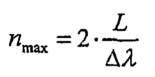
und beträgt in diesem Falle nmax=13. Ist die Anzahl der Verschiebungen größer als nmax so werden die Spektralkomponenten zu häufig abgetastet und es ergibt sich kein weiterer Auflösungsgewinn. Ist n kleiner als nmax so werden zu wenige Spektralkomponenten abgetastet und die Auflösung der Detektionseinheit wird durch den Detektor festgelegt.
and is in this case n max = 13. If the number of shifts is greater than n max , the spectral components are sampled too frequently and there is no further resolution gain. If n is smaller than n max , too few spectral components are scanned and the resolution of the detection unit is determined by the detector.
Eine Anordnung zum Auslesen der Einzelkanäle ck,j in Abhängigkeit vom Drehwinkel phi des Gitters bzw. des Spiegels ist in Abb._11 schematisch dargestellt. Hierbei wird der an den Anoden des PMT fließende Strom, jeweils durch den ersten Amplifier A (als Strom-Spannungswandler geschaltet) in eine Spannung gewandelt und verstärkt. Die Spannung wird einem Integrator I zugeführt der über eine entsprechende Zeit (z.B. Pixelverweilzeit) das Signal integriert.An arrangement for reading the individual channels c k, j as a function of the rotation angle phi of the grating or the mirror is shown schematically in Fig._11 . In this case, the current flowing at the anodes of the PMT, in each case by the first amplifier A (connected as a current-voltage converter) is converted into a voltage and amplified. The voltage is fed to an integrator I which integrates the signal over a corresponding time (eg pixel dwell time).
Zur schnelleren Auswertung kann dem Integrator I ein Komparator K nachgeschaltet werden, der als einfacher Komparator eine Schaltschwelle hat, die bei Überschreitung ein digitales Ausgangssignal erzeugt oder der als Fensterkomparator ausgebildet ist und dann ein digitales Ausgangssignal bildet, wenn sich das Eingangssignal zwischen der oberen und unteren Schaltschwelle befindet oder wenn das Eingangssignal außerhalb (unter oder über) den Schaltschwellen liegt. Die Anordnung des Komparators bzw. des Fensterkomparators kann sowohl vor dem Integrator als auch danach erfolgen. Schaltungsanordnungen ohne Integrator (so genannte Verstärkermode) sind ebenfalls denkbar. Bei der Anordnung im Verstärkermode wird der Komparator K weiterhin nach entsprechender Pegelanpassung verwendet. Der Ausgang des Komparators K dient als Steuersignal für ein Switch-Register Reg, das direkt die aktiven Kanäle schaltet (online) oder der Zustand wird dem Computer über eine zusätzliche Verbindung V mitgeteilt, um eine individuelle Auswahl der aktiven Kanäle zu treffen (off-line). Das Ausgangssignal des Integrators I wird direkt einem weiteren Ampl. A1 zur Pegelanpassung, für die nachfolgende A/D-Wandlung AD zugeführt. Die AD gewandelten Werte werden über geeignete Datenübertragung an einen Rechner (PC oder Digital-Signal-Prozessor DSP) übertragen.For faster evaluation, the integrator I, a comparator K are connected downstream, which has a switching threshold as a simple comparator, which generates a digital output signal when exceeded or is designed as a window comparator and then forms a digital output signal when the input signal between the upper and lower Switching threshold or if the input signal is outside (below or above) the switching thresholds. The arrangement of the comparator or the window comparator can be done both before the integrator and afterwards. Circuit arrangements without integrator (so-called amplifier mode) are also conceivable. When arranged in the Amplifier mode, the comparator K continues to be used after appropriate level adjustment. The output of the comparator K serves as a control signal for a switch register Reg which directly switches the active channels (online) or the state is communicated to the computer via an additional connection V to make an individual selection of the active channels (off-line ). The output signal of the integrator I is directly another Ampl. A1 for level adjustment, supplied for the subsequent A / D conversion AD. The AD converted values are transmitted via suitable data transmission to a computer (PC or Digital Signal Processor DSP).
Eine Änderung des Drehwinkels phi bzw. der Verschiebung dl kann bildweise nach der Aufnahme oder während des Scannens eines Bildpunktes bzw. einer Bildzeile / -spalte erfolgen Die mechanischen Anfordungen an die Scangeschwindigkeit des Wellenlängen- bzw. Positionsscanners (WS) hängen von der Art der Einstellung des Drehwinkels ab. Erfolgt beispielsweise eine bildpunktweise Erhöhung der spektralen oder räumlichen Detektorauflösung so muß der Scan innerhalb der Integrationszeit für diesen Bildpunkt erfolgen (also in einigen Mikrosekunden). Erfolgt die Erhöhung der Detektorauflösung bildweise so muß die Scan innerhalb von einigen Millisekungen bis Sekunden erfolgen. Die Abfolge der Einstellung des Drehwinkels kann beispielsweise bei einer 5 maligen Verschiebung in der Reihenfolge von j=0,2,4,3,1 erfolgen. In diesem Falle wird um j*L/5 (bezogen auf die Ausgangsposition für j=0) verschoben. Diese Reihenfolge hat den Vorteil, dass Zwischenwerte schon nach der Aufnahme der Einzelkanäle für j=0,2 und 4 berechnet und dargestellt werden können. Im Anschluß werden dann die verbleibenden Einzelkanäle für j=1,3 gemessen und die restlichen Zwischenwerte berechnet und damit die Meßkurve in ihrer Auflösung weiter schrittweise verfeinert.A change in the angle of rotation phi or the displacement dl can take place imagewise after recording or during the scanning of a pixel or image row / column. The mechanical requirements for the scanning speed of the wavelength or position scanner (WS) depend on the type of adjustment of the angle of rotation. If, for example, a pixel-by-pixel increase in the spectral or spatial detector resolution occurs, then the scan must take place within the integration time for this pixel (ie in a few microseconds). If the increase in the detector resolution is imagewise, the scan must take place within a few milliseconds to seconds. The sequence of adjustment of the rotation angle can be done, for example, with a 5-times shift in the order of j = 0,2,4,3,1. In this case, it is shifted by j * L / 5 (relative to the starting position for j = 0). This order has the advantage that intermediate values can already be calculated and displayed after recording the individual channels for j = 0.2 and 4. Then, the remaining individual channels are measured for j = 1.3 and the remaining intermediate values are calculated and the resolution of the measurement curve is further refined step by step.
In einer weiteren Anordnung nach
In der oben beschriebenen Anordnung wurde eine Integratorschaltung zur Detektion der Einzelkanalsignale verwendet. Uneingeschränkt kann jedoch auch eine Photonenzählung in den Einzelkanälen erfolgen.In the above-described arrangement, an integrator circuit was used to detect the single channel signals. Unrestricted, however, can also be done a photon count in the individual channels.
Der o.g. Zeilen- bzw. Matrixdetektor von Hamamatsu besitzt zwischen den aneinander grenzenden Einzelkanälen Stege mit einer Breite von 0.2 mm. Diese Stege wirken sich negativ auf den Berechnungsalgorithmus und auf die Effizienz der Detektionseinrichtung aus. Zur Vermeidung dieses Effektes kann ggf. vor dem Zeilen- bzw. Matrixdetektor ein Mikrolinsenarray nach dem Stand der Technik angeordnet werden. Dieses Linsenarray fokussiert zusätzlich das ankommende Licht auf die aktiven Bereichen (Einzelkanäle) des Zeilen- bzw. Matrixdetektors. Weiterhin wird das Übersprechen zwischen angrenzenden Einzelkanälen minimiert.The o.g. Hamamatsu line or matrix detector has webs with a width of 0.2 mm between the adjacent individual channels. These webs have a negative effect on the calculation algorithm and on the efficiency of the detection device. To avoid this effect, a microlens array according to the prior art may optionally be arranged in front of the line or matrix detector. This lens array additionally focuses the incoming light on the active areas (single channels) of the line or matrix detector. Furthermore, crosstalk between adjacent single channels is minimized.
In
In
Claims (40)
- Method for optically acquiring characteristic variables of an illuminated sample in a laser scanning microsope, a reflected and/or fluoresced and/or transmitted radiation backscattered by the sample being detected with the aid of a spatially resolving detector by imaging the radiation coming from the sample onto the detector, and a spectrally resolved measurement being made of the radiation coming from the sample via a dispersive element upstream of the detector, characterized in that the position of the spatially resolved measured radiation is displaced relative to the detector, the step size of the displacement being below the grid size of the spatial resolution of the detector, and an algorithm being used to determine intermediate values from the signals measured for various displacements in order to increase the spatial resolution of the detector and the intermediate values thus calculated being represented graphically on a displayed image.
- Method according to Claim 1, in which there occurs a displacement of the detector in the direction of its spatial resolution, and/or a displacement or pivoting of an imaging element on at least one axis, and/or of a reflective element on at least one axis, and/or of a dispersive element on at least one axis.
- Method according to Claim 2, in which, given a stationary dispersive element on at least one of its pivoting axes, the spatially varying effect of the pivoting on this axis is produced by a scanning unit and/or displacement of the detector.
- Method according to Claim 2, in which, given a line scanner for real time microscopy, a displacement is performed by a mirror which can be pivoted about at least one axis, and/or by a displacement of the detector, and/or by a mirror of a scanning mirror arrangement.
- Method according to Claim 2, in which, given a stationary mirror, pivoting is performed by a scanning unit and/or displacement of the detector.
- Method according to Claim 4, in which a switchover is made between a line scan and a dispersive splitting.
- Method according to one of Claims 1-6, in which the dispersive element is pivoted in order to increase the spectral resolution and, furthermore, an additional movement of the detector and/or a scanning unit occurs.
- Method according to one of Claims 1-7, in which the signals are converted by detection channels and read out digitally, and the calculation of the algorithm is performed digitally in a computer.
- Method according to one of Claims 1-8, in which the signals of the detection channels are influenced by a nonlinear distortion of the input signals.
- Method according to Claim 9, in which integration parameters are influenced.
- Method according to Claim 9, in which the characteristic curve of an amplifier is influenced.
- Method according to one of Claims 1-11, in which the calculated intermediate values and/or detected signals are used to generate an image.
- Method according to Claim 12, in which a colour-coded fluorescence image is generated.
- Method according to Claim 12 or 13, in which overlaying with further images occurs.
- Method according to one of Claims 1-14, in which comparators in detection channels are used to compare the measured signal with a reference signal and, in the case of an under-shooting and/or overshooting of the reference signal, the operating mode of the detection channel is changed.
- Method according to Claim 15, in which the respective detection channel is switched off and/or not taken into account.
- Method according to one of Claims 1-16, in which the signals of the detection channels are respectively generated by means of at least one integrator circuit.
- Method according to one of Claims 1-16, in which the signals of the detection channels are generated by means of photon counting and subsequent digital/analogue conversion.
- Method according to Claim 18, in which the photon counting is performed in a time-correlated fashion.
- Method according to one of Claims 1-19, characterized by its use for optically acquiring characteristic variables of the wavelength-dependent behaviour of an illuminated sample, in particular the emission and/or absorption behaviour, preferably the fluorescence and/or luminescence and/or phosphorescence and/or enzyme-activated light emission and/or enzyme-activated fluorescence.
- Method according to one of the Claims 1-19, characterized by its use in distinguishing various dyes and/or in determining the local dye composition of a pixel given simultaneous use of a plurality of dyes, and/or in determining the local displacement of the emission spectrum as a function of the local environment with which the dye/dyes is/are associated and/or in measuring emission ratio dyes in order to determine ion concentrations.
- Method according to one of the Claims 1-19, characterized by its use in distinguishing various dyes and/or in determining the local dye composition of a pixel given simultaneous use of a plurality of dyes, and/or in determining the local displacement of the absorption spectrum as a function of the local environment with which the dye/dyes is/are associated and/or in measuring the absorption ratio in order to determine ion concentrations.
- Method according to one of Claims 1-19, characterized by its use in acquiring single-photon and/or multiphoton fluorescence, and/or by entangled-photon-excited fluorescence.
- Method according to one of Claims 1-19, characterized by its use in parallel illumination and detection, preferably in active-substance screening, the sample preferably being a microtitre plate.
- Method according to one of Claims 1-19, characterized by its use in detecting in a scanning near-field microscope.
- Method according to one of Claims 1-19, characterized by its use in detecting a single-photon and/or multiphoton dye fluorescence in a fluorescence-correlated spectroscope.
- Laser-scanning microscope for optically acquiring characteristic variables of an illuminated sample, having a spatially resolving detector for detecting the radiation backscattered, reflected and/or fluoresced and/or transmitted by the sample, an imaging element for imaging the radiation coming from the sample onto the detector, and a dispersive element arranged upstream of the detector for spectrally resolved measurement, characterized in that in order to displace the position of the spatially resolved measured radiation relative to the detector, the detector is designed to be displaceable in the direction of its spatial resolution, and/or the imaging element is designed to be displaceable on at least one axis, and/or a reflective element is designed to be displaceable on at least one axis, and/or the dispersive element is designed to be displaceable on at least one axis, the step size of the displacement being below the grid size of he spatial resolution of the detector, and in that means are provided in order to use an algorithm to determine intermediate values from the signals measured for various displacements in order to increase the spatial resolution of the detector, and to represent these intermediate values graphically on a displayed image.
- Laser scanning microscope according to Claim 27, in which the dispersive element is designed to be able to pivot about at least one axis.
- Laser scanning microscope according to Claim 27, in which, given a stationary dispersive element on at least one of its pivoting axes, the spatially varying effect of the pivoting on this axis is produced by a scanning unit.
- Laser scanning microscope according to Claim 27, in which, given a line scanner for real time microscopy, a mirror which can be pivoted about at least one axis, and/or a displacement detector and/or a mirror of a scanning mirror arrangement are/is provided for the displacement.
- Laser scanning microscope according to Claim 27, in which a stationary mirror and a scanning unit are provided for pivoting on a pivoting axis.
- Laser scanning microscope according to one of Claims 27-31 which is designed to acquire single-photon and/or multiphoton fluorescence and/or entangled-photon-excited fluorescence.
- Laser scanning microscope according to one of Claims 27-31 which is designed for parallel illumination and detection, preferably in active-substance screening, the sample preferably being a microtitre plate.
- Laser scanning microscope according to one of Claims 27-31 which is designed as a scanning near-field microscope.
- Laser scanning microscope according to one of Claims 27-31 which is designed to detect a single-photon and/or multiphoton dye fluorescence in a fluorescence-correlated spectroscope.
- Laser scanning microscope according to one of Claims 27-35 with confocal detection.
- Laser scanning microscope according to one of Claims 27-36 with an X/Y scanner in the illumination.
- Laser scanning microscope according to one of Claims 27-37 with an X/Y scanning table.
- Laser scanning microscope according to one of Claims 27-38 with non-confocal detection.
- Laser scanning microscope according to one of Claims 27-31 with bright-field imaging.
Applications Claiming Priority (3)
| Application Number | Priority Date | Filing Date | Title |
|---|---|---|---|
| DE10038528 | 2000-08-08 | ||
| DE10038528A DE10038528A1 (en) | 2000-08-08 | 2000-08-08 | Optical detection of characteristic parameters of illuminated specimen involves computing intermediate values from signals for different displacements to increase spatial resolution |
| PCT/EP2001/009050 WO2002012864A1 (en) | 2000-08-08 | 2001-08-04 | Method and assembly for increasing the spectral and spatial resolution of a detector |
Publications (2)
| Publication Number | Publication Date |
|---|---|
| EP1264169A1 EP1264169A1 (en) | 2002-12-11 |
| EP1264169B1 true EP1264169B1 (en) | 2009-09-30 |
Family
ID=7651623
Family Applications (1)
| Application Number | Title | Priority Date | Filing Date |
|---|---|---|---|
| EP01958054A Expired - Lifetime EP1264169B1 (en) | 2000-08-08 | 2001-08-04 | Improvement of spectral and/or spatial resolution in a laser scanning microscope |
Country Status (5)
| Country | Link |
|---|---|
| EP (1) | EP1264169B1 (en) |
| JP (2) | JP2004506192A (en) |
| AT (1) | ATE444483T1 (en) |
| DE (2) | DE10038528A1 (en) |
| WO (1) | WO2002012864A1 (en) |
Families Citing this family (38)
| Publication number | Priority date | Publication date | Assignee | Title |
|---|---|---|---|---|
| DE10102033C5 (en) * | 2001-01-18 | 2011-01-13 | Leica Microsystems Cms Gmbh | Device and scanning microscope for the simultaneous detection of multiple spectral regions of a light beam |
| DE10151216A1 (en) * | 2001-10-16 | 2003-04-24 | Zeiss Carl Jena Gmbh | Method for the optical detection of characteristic quantities of an illuminated sample |
| DE10222779A1 (en) * | 2002-05-16 | 2004-03-04 | Carl Zeiss Jena Gmbh | Method and arrangement for examining samples |
| DE10254139A1 (en) * | 2002-11-15 | 2004-05-27 | Carl Zeiss Jena Gmbh | Method and arrangement for the depth-resolved optical detection of a sample |
| WO2005114291A1 (en) * | 2004-05-12 | 2005-12-01 | Beth Israel Deaconess Medical Center, Inc. | Method and apparatus for detecting microscopic objects |
| JP4529587B2 (en) | 2004-08-23 | 2010-08-25 | 株式会社ニコン | Spectroscopic apparatus and spectral laser microscope |
| JP4800655B2 (en) | 2005-04-01 | 2011-10-26 | オリンパス株式会社 | Light measuring device |
| DE102005046754A1 (en) * | 2005-09-29 | 2007-04-05 | Carl Zeiss Jena Gmbh | Specimen sensing device e.g. laser scanning microscope, has control unit alternatively connecting each recording pixel to analysis channels, such that detected light is divided into two portions phased in relation to one another |
| DE102009038028A1 (en) | 2009-08-18 | 2011-02-24 | Carl Zeiss Microlmaging Gmbh | Detector arrangement with increased sensitivity |
| DE102009059280A1 (en) * | 2009-12-22 | 2011-06-30 | Leibniz-Institut für Analytische Wissenschaften-ISAS-e.V., 44139 | spectrometer arrangement |
| CN102782479B (en) * | 2010-03-01 | 2014-04-30 | 奥林巴斯株式会社 | Optical analysis device, optical analysis method |
| JP5877155B2 (en) | 2010-07-26 | 2016-03-02 | オリンパス株式会社 | Method for detecting dilute particles in solution using luminescent probe |
| CN103221806B (en) | 2010-09-10 | 2015-11-25 | 奥林巴斯株式会社 | Use the optical analysis method of the measurement of the light of plural wavelength band |
| WO2012032981A1 (en) | 2010-09-10 | 2012-03-15 | オリンパス株式会社 | Optical analysis method using optical intensity of single light-emitting particle |
| JP5907882B2 (en) | 2010-10-19 | 2016-04-26 | オリンパス株式会社 | Optical analyzer for observing polarization characteristics of single luminescent particles, optical analysis method, and computer program for optical analysis therefor |
| CN103229042B (en) | 2010-11-25 | 2016-06-29 | 奥林巴斯株式会社 | The light analytical equipment and the light that utilize the wavelength characteristic of the light of single incandescnet particle analyze method |
| WO2012099234A1 (en) | 2011-01-20 | 2012-07-26 | オリンパス株式会社 | Photoanalysis method and photoanalysis device using detection of light from single light-emitting particle |
| JP6009944B2 (en) | 2011-01-26 | 2016-10-19 | オリンパス株式会社 | Nucleic acid molecule polymorphism identification method |
| EP2669663B1 (en) | 2011-01-26 | 2017-09-27 | Olympus Corporation | Method for identifying polymorphism of nucleic acid molecules |
| WO2012133292A1 (en) | 2011-03-29 | 2012-10-04 | オリンパス株式会社 | Photometric analysis device, photometric analysis method, and computer program for photometric analysis, using single light-emitting particle detection |
| CN103477210B (en) | 2011-04-13 | 2015-09-23 | 奥林巴斯株式会社 | The light analytical equipment utilizing single incandescnet particle to detect, light analytical approach and light analysis computer program |
| EP2700935A4 (en) | 2011-04-18 | 2014-10-22 | Olympus Corp | Quantitative determination method for target particles, photometric analysis device, and computer program for photometric analysis |
| JP6013335B2 (en) | 2011-08-11 | 2016-10-25 | オリンパス株式会社 | Target particle counting method |
| JP6013337B2 (en) | 2011-08-15 | 2016-10-25 | オリンパス株式会社 | Optical analysis apparatus using single luminescent particle detection, optical analysis method, and computer program for optical analysis |
| JP6013338B2 (en) | 2011-08-26 | 2016-10-25 | オリンパス株式会社 | Optical analysis apparatus using single luminescent particle detection, optical analysis method, and computer program for optical analysis |
| JP6010033B2 (en) | 2011-08-26 | 2016-10-19 | オリンパス株式会社 | Single particle detection apparatus using optical analysis, single particle detection method, and computer program for single particle detection |
| JP6010034B2 (en) | 2011-08-30 | 2016-10-19 | オリンパス株式会社 | Target particle detection method |
| EP2752654A4 (en) | 2011-08-30 | 2015-04-15 | Olympus Corp | Optical analyzer using single light-emitting particle detection, optical analysis method, and computer program for optical analysis |
| WO2013069504A1 (en) | 2011-11-10 | 2013-05-16 | オリンパス株式会社 | Spectroscopy device, spectroscopy method, and computer program for spectroscopy, employing individual light-emitting particle detection |
| JP5996625B2 (en) | 2012-02-17 | 2016-09-21 | オリンパス株式会社 | Optical analysis apparatus using single particle detection, optical analysis method, and computer program for optical analysis |
| JP5940644B2 (en) | 2012-02-22 | 2016-06-29 | オリンパス株式会社 | Target particle detection method |
| WO2013140890A1 (en) | 2012-03-21 | 2013-09-26 | オリンパス株式会社 | Method for detecting target nucleic acid molecule |
| JP6010114B2 (en) | 2012-04-18 | 2016-10-19 | オリンパス株式会社 | Single particle detection apparatus using optical analysis, single particle detection method, and computer program for single particle detection |
| CN104136915B (en) | 2012-04-18 | 2016-07-13 | 奥林巴斯株式会社 | The detection method of intended particle |
| CN105431759B (en) | 2013-07-31 | 2018-04-13 | 奥林巴斯株式会社 | Utilize the optical microphotograph lens device of single incandescnet particle detection technique, microscopic observation and computer program for micro- sem observation |
| JP6313776B2 (en) | 2013-10-07 | 2018-04-18 | オリンパス株式会社 | Optical analysis apparatus using single luminescent particle detection, optical analysis method, and computer program for optical analysis |
| WO2017098597A1 (en) | 2015-12-09 | 2017-06-15 | オリンパス株式会社 | Optical analysis method and optical analysis device employing single light-emitting particle detection |
| CN114112041B (en) * | 2021-11-24 | 2023-07-25 | 中国工程物理研究院激光聚变研究中心 | Spectral imaging system based on micro-nano optical filter array and scanning method thereof |
Citations (4)
| Publication number | Priority date | Publication date | Assignee | Title |
|---|---|---|---|---|
| EP0320530A1 (en) * | 1987-12-18 | 1989-06-21 | Hewlett-Packard GmbH | Photodiode array spectrometer |
| DE4017317A1 (en) * | 1990-05-30 | 1991-12-05 | Bodenseewerk Perkin Elmer Co | System for enhancing spectrometer resolution - shifts spectrum periodically relative to detector array |
| US5192980A (en) * | 1990-06-27 | 1993-03-09 | A. E. Dixon | Apparatus and method for method for spatially- and spectrally-resolved measurements |
| US6088097A (en) * | 1998-01-14 | 2000-07-11 | Uhl; Rainer | Point-scanning luminescent microscope |
Family Cites Families (8)
| Publication number | Priority date | Publication date | Assignee | Title |
|---|---|---|---|---|
| DE69227201T2 (en) * | 1991-11-16 | 1999-02-18 | Renishaw Plc | Spectroscopic method |
| JPH0682305A (en) * | 1992-08-31 | 1994-03-22 | Shimadzu Corp | Two-dimensional detector |
| DE4307833A1 (en) * | 1993-03-12 | 1994-09-15 | Thomson Video Europ Gmbh | Video camera with a semiconductor sensor |
| JP3095970B2 (en) * | 1995-02-06 | 2000-10-10 | 日本分光株式会社 | Deconvolution processing method and apparatus |
| JP2888813B2 (en) * | 1997-08-29 | 1999-05-10 | 株式会社東芝 | High resolution pixel output method and apparatus |
| ATE272224T1 (en) * | 1997-11-17 | 2004-08-15 | Max Planck Gesellschaft | CONFOCAL SPECTROSCOPY SYSTEM AND METHOD |
| JPH11190695A (en) * | 1997-12-26 | 1999-07-13 | Hitachi Ltd | Semiconductor stress measuring raman spectrophotometer |
| DE20008133U1 (en) * | 2000-05-05 | 2000-07-27 | Chang Rong Seng | Sensor matrix resolution improvement arrangement |
-
2000
- 2000-08-08 DE DE10038528A patent/DE10038528A1/en not_active Withdrawn
-
2001
- 2001-08-04 WO PCT/EP2001/009050 patent/WO2002012864A1/en active Application Filing
- 2001-08-04 EP EP01958054A patent/EP1264169B1/en not_active Expired - Lifetime
- 2001-08-04 AT AT01958054T patent/ATE444483T1/en not_active IP Right Cessation
- 2001-08-04 DE DE50115136T patent/DE50115136D1/en not_active Expired - Lifetime
- 2001-08-04 JP JP2002517498A patent/JP2004506192A/en active Pending
-
2006
- 2006-01-11 JP JP2006003328A patent/JP4783931B2/en not_active Expired - Fee Related
Patent Citations (4)
| Publication number | Priority date | Publication date | Assignee | Title |
|---|---|---|---|---|
| EP0320530A1 (en) * | 1987-12-18 | 1989-06-21 | Hewlett-Packard GmbH | Photodiode array spectrometer |
| DE4017317A1 (en) * | 1990-05-30 | 1991-12-05 | Bodenseewerk Perkin Elmer Co | System for enhancing spectrometer resolution - shifts spectrum periodically relative to detector array |
| US5192980A (en) * | 1990-06-27 | 1993-03-09 | A. E. Dixon | Apparatus and method for method for spatially- and spectrally-resolved measurements |
| US6088097A (en) * | 1998-01-14 | 2000-07-11 | Uhl; Rainer | Point-scanning luminescent microscope |
Also Published As
| Publication number | Publication date |
|---|---|
| EP1264169A1 (en) | 2002-12-11 |
| ATE444483T1 (en) | 2009-10-15 |
| JP2006153891A (en) | 2006-06-15 |
| DE50115136D1 (en) | 2009-11-12 |
| DE10038528A1 (en) | 2002-02-21 |
| WO2002012864A1 (en) | 2002-02-14 |
| JP2004506192A (en) | 2004-02-26 |
| JP4783931B2 (en) | 2011-09-28 |
Similar Documents
| Publication | Publication Date | Title |
|---|---|---|
| EP1264169B1 (en) | Improvement of spectral and/or spatial resolution in a laser scanning microscope | |
| EP1307726B2 (en) | Method for detecting the wavelength-dependent behavior of an illuminated specimen | |
| EP1504300B1 (en) | Method and arrangement for analyzing samples | |
| EP1248132B1 (en) | Method and arrangement for depth resolving optical detection of a probe | |
| DE10257237B4 (en) | Arrangement for the optical detection of light radiation excited and / or backscattered in a sample | |
| EP2641078B1 (en) | Microscopy with improved depth resolution | |
| EP3033645B1 (en) | High-resolution scanning microscopy | |
| DE10151217B4 (en) | Method for operating a laser scanning microscope | |
| EP1396739B1 (en) | Method and arrangement for adjustable modulation of spectral composition and/or intensity of pump light and/or probe light | |
| EP1302804A2 (en) | Method for the optical determination of characteristical parameters of a sample | |
| DE10004191B4 (en) | Fluorescence scanning microscope | |
| DE10033180B4 (en) | Method for the detection of dyes in fluorescence microscopy | |
| US20020036775A1 (en) | Method for increasing the spectral and spatial resolution of detectors | |
| DE102013019348A1 (en) | High-resolution scanning microscopy | |
| WO2011085766A1 (en) | High-resolution microscope and method for determining the two- or three-dimensional positions of objects | |
| DE102015107367A1 (en) | Evaluation of Fluorescence Scanning Microscopy Signals Using a Confocal Laser Scanning Microscope | |
| DE10155002A1 (en) | Depth-resolved optical imaging method for use in biological scanning microscopy, uses phase or frequency modulation of the imaging light | |
| DE10118463A1 (en) | Depth-resolved optical imaging method for use in biological scanning microscopy, uses phase or frequency modulation of the imaging light | |
| DE10227111A1 (en) | Spectral microscope and method for data acquisition with a spectral microscope | |
| EP1273951B1 (en) | Scanning microscope and method for the wavelength dependent detection | |
| EP4189358A1 (en) | Method for detecting emission light, detection device and laser scanning microscope | |
| WO2004113987A1 (en) | Method to be used in fluorescence microscopy | |
| EP3992688A1 (en) | Device and method for detecting image data |
Legal Events
| Date | Code | Title | Description |
|---|---|---|---|
| PUAI | Public reference made under article 153(3) epc to a published international application that has entered the european phase |
Free format text: ORIGINAL CODE: 0009012 |
|
| 17P | Request for examination filed |
Effective date: 20020624 |
|
| AK | Designated contracting states |
Kind code of ref document: A1 Designated state(s): AT BE CH CY DE DK ES FI FR GB GR IE IT LI LU MC NL PT SE TR |
|
| RIN1 | Information on inventor provided before grant (corrected) |
Inventor name: MOEHLER, GUNTER Inventor name: WOLLESCHENSKY, RALF Inventor name: GERSTNER, VOLKER |
|
| 17Q | First examination report despatched |
Effective date: 20040204 |
|
| GRAP | Despatch of communication of intention to grant a patent |
Free format text: ORIGINAL CODE: EPIDOSNIGR1 |
|
| RIC1 | Information provided on ipc code assigned before grant |
Ipc: G02B 21/36 20060101ALI20090313BHEP Ipc: G01N 21/64 20060101ALI20090313BHEP Ipc: G02B 21/16 20060101ALI20090313BHEP Ipc: G01N 21/27 20060101AFI20090313BHEP Ipc: G01N 21/47 20060101ALI20090313BHEP Ipc: G02B 21/00 20060101ALI20090313BHEP |
|
| RTI1 | Title (correction) |
Free format text: IMPROVEMENT OF SPECTRAL AND/OR SPATIAL RESOLUTION IN A LASER SCANNING MICROSCOPE |
|
| RIN1 | Information on inventor provided before grant (corrected) |
Inventor name: WOLLESCHENSKY, RALF Inventor name: GERSTNER, VOLKER Inventor name: MOEHLER, GUNTER |
|
| GRAS | Grant fee paid |
Free format text: ORIGINAL CODE: EPIDOSNIGR3 |
|
| GRAA | (expected) grant |
Free format text: ORIGINAL CODE: 0009210 |
|
| RIN1 | Information on inventor provided before grant (corrected) |
Inventor name: MOEHLER, GUNTER Inventor name: WOLLESCHENSKY, RALF Inventor name: GERSTNER, VOLKER |
|
| RAP1 | Party data changed (applicant data changed or rights of an application transferred) |
Owner name: CARL ZEISS MICROIMAGING GMBH |
|
| AK | Designated contracting states |
Kind code of ref document: B1 Designated state(s): AT BE CH CY DE DK ES FI FR GB GR IE IT LI LU MC NL PT SE TR |
|
| REG | Reference to a national code |
Ref country code: CH Ref legal event code: EP Ref country code: GB Ref legal event code: FG4D Free format text: NOT ENGLISH |
|
| REG | Reference to a national code |
Ref country code: IE Ref legal event code: FG4D |
|
| REF | Corresponds to: |
Ref document number: 50115136 Country of ref document: DE Date of ref document: 20091112 Kind code of ref document: P |
|
| PG25 | Lapsed in a contracting state [announced via postgrant information from national office to epo] |
Ref country code: SE Free format text: LAPSE BECAUSE OF FAILURE TO SUBMIT A TRANSLATION OF THE DESCRIPTION OR TO PAY THE FEE WITHIN THE PRESCRIBED TIME-LIMIT Effective date: 20090930 Ref country code: FI Free format text: LAPSE BECAUSE OF FAILURE TO SUBMIT A TRANSLATION OF THE DESCRIPTION OR TO PAY THE FEE WITHIN THE PRESCRIBED TIME-LIMIT Effective date: 20090930 |
|
| NLV1 | Nl: lapsed or annulled due to failure to fulfill the requirements of art. 29p and 29m of the patents act | ||
| PG25 | Lapsed in a contracting state [announced via postgrant information from national office to epo] |
Ref country code: PT Free format text: LAPSE BECAUSE OF FAILURE TO SUBMIT A TRANSLATION OF THE DESCRIPTION OR TO PAY THE FEE WITHIN THE PRESCRIBED TIME-LIMIT Effective date: 20100201 Ref country code: ES Free format text: LAPSE BECAUSE OF FAILURE TO SUBMIT A TRANSLATION OF THE DESCRIPTION OR TO PAY THE FEE WITHIN THE PRESCRIBED TIME-LIMIT Effective date: 20100110 |
|
| REG | Reference to a national code |
Ref country code: IE Ref legal event code: FD4D |
|
| PG25 | Lapsed in a contracting state [announced via postgrant information from national office to epo] |
Ref country code: CY Free format text: LAPSE BECAUSE OF FAILURE TO SUBMIT A TRANSLATION OF THE DESCRIPTION OR TO PAY THE FEE WITHIN THE PRESCRIBED TIME-LIMIT Effective date: 20090930 |
|
| PG25 | Lapsed in a contracting state [announced via postgrant information from national office to epo] |
Ref country code: NL Free format text: LAPSE BECAUSE OF FAILURE TO SUBMIT A TRANSLATION OF THE DESCRIPTION OR TO PAY THE FEE WITHIN THE PRESCRIBED TIME-LIMIT Effective date: 20090930 Ref country code: IE Free format text: LAPSE BECAUSE OF FAILURE TO SUBMIT A TRANSLATION OF THE DESCRIPTION OR TO PAY THE FEE WITHIN THE PRESCRIBED TIME-LIMIT Effective date: 20090930 Ref country code: DK Free format text: LAPSE BECAUSE OF FAILURE TO SUBMIT A TRANSLATION OF THE DESCRIPTION OR TO PAY THE FEE WITHIN THE PRESCRIBED TIME-LIMIT Effective date: 20090930 |
|
| PLBE | No opposition filed within time limit |
Free format text: ORIGINAL CODE: 0009261 |
|
| STAA | Information on the status of an ep patent application or granted ep patent |
Free format text: STATUS: NO OPPOSITION FILED WITHIN TIME LIMIT |
|
| 26N | No opposition filed |
Effective date: 20100701 |
|
| PG25 | Lapsed in a contracting state [announced via postgrant information from national office to epo] |
Ref country code: GR Free format text: LAPSE BECAUSE OF FAILURE TO SUBMIT A TRANSLATION OF THE DESCRIPTION OR TO PAY THE FEE WITHIN THE PRESCRIBED TIME-LIMIT Effective date: 20091231 |
|
| BERE | Be: lapsed |
Owner name: CARL ZEISS MICROLMAGING G.M.B.H. Effective date: 20100831 |
|
| PG25 | Lapsed in a contracting state [announced via postgrant information from national office to epo] |
Ref country code: MC Free format text: LAPSE BECAUSE OF NON-PAYMENT OF DUE FEES Effective date: 20100831 Ref country code: IT Free format text: LAPSE BECAUSE OF FAILURE TO SUBMIT A TRANSLATION OF THE DESCRIPTION OR TO PAY THE FEE WITHIN THE PRESCRIBED TIME-LIMIT Effective date: 20090930 |
|
| REG | Reference to a national code |
Ref country code: CH Ref legal event code: PL |
|
| PG25 | Lapsed in a contracting state [announced via postgrant information from national office to epo] |
Ref country code: LI Free format text: LAPSE BECAUSE OF NON-PAYMENT OF DUE FEES Effective date: 20100831 Ref country code: CH Free format text: LAPSE BECAUSE OF NON-PAYMENT OF DUE FEES Effective date: 20100831 |
|
| PG25 | Lapsed in a contracting state [announced via postgrant information from national office to epo] |
Ref country code: BE Free format text: LAPSE BECAUSE OF NON-PAYMENT OF DUE FEES Effective date: 20100831 |
|
| PG25 | Lapsed in a contracting state [announced via postgrant information from national office to epo] |
Ref country code: AT Free format text: LAPSE BECAUSE OF NON-PAYMENT OF DUE FEES Effective date: 20100804 |
|
| PG25 | Lapsed in a contracting state [announced via postgrant information from national office to epo] |
Ref country code: LU Free format text: LAPSE BECAUSE OF NON-PAYMENT OF DUE FEES Effective date: 20100804 |
|
| PG25 | Lapsed in a contracting state [announced via postgrant information from national office to epo] |
Ref country code: TR Free format text: LAPSE BECAUSE OF FAILURE TO SUBMIT A TRANSLATION OF THE DESCRIPTION OR TO PAY THE FEE WITHIN THE PRESCRIBED TIME-LIMIT Effective date: 20090930 |
|
| REG | Reference to a national code |
Ref country code: DE Ref legal event code: R081 Ref document number: 50115136 Country of ref document: DE Owner name: CARL ZEISS MICROSCOPY GMBH, DE Free format text: FORMER OWNER: CARL ZEISS MICROIMAGING GMBH, 07745 JENA, DE Effective date: 20130204 |
|
| PGFP | Annual fee paid to national office [announced via postgrant information from national office to epo] |
Ref country code: FR Payment date: 20140821 Year of fee payment: 14 Ref country code: GB Payment date: 20140820 Year of fee payment: 14 |
|
| PGFP | Annual fee paid to national office [announced via postgrant information from national office to epo] |
Ref country code: DE Payment date: 20150821 Year of fee payment: 15 |
|
| GBPC | Gb: european patent ceased through non-payment of renewal fee |
Effective date: 20150804 |
|
| REG | Reference to a national code |
Ref country code: FR Ref legal event code: ST Effective date: 20160429 |
|
| PG25 | Lapsed in a contracting state [announced via postgrant information from national office to epo] |
Ref country code: GB Free format text: LAPSE BECAUSE OF NON-PAYMENT OF DUE FEES Effective date: 20150804 |
|
| PG25 | Lapsed in a contracting state [announced via postgrant information from national office to epo] |
Ref country code: FR Free format text: LAPSE BECAUSE OF NON-PAYMENT OF DUE FEES Effective date: 20150831 |
|
| REG | Reference to a national code |
Ref country code: DE Ref legal event code: R119 Ref document number: 50115136 Country of ref document: DE |
|
| PG25 | Lapsed in a contracting state [announced via postgrant information from national office to epo] |
Ref country code: DE Free format text: LAPSE BECAUSE OF NON-PAYMENT OF DUE FEES Effective date: 20170301 |