EP1263140A2 - Schaltungsanordnung zur Erzeugung von kurzen Laserimpulsen mit einer Laserdiode - Google Patents
Schaltungsanordnung zur Erzeugung von kurzen Laserimpulsen mit einer Laserdiode Download PDFInfo
- Publication number
- EP1263140A2 EP1263140A2 EP02010393A EP02010393A EP1263140A2 EP 1263140 A2 EP1263140 A2 EP 1263140A2 EP 02010393 A EP02010393 A EP 02010393A EP 02010393 A EP02010393 A EP 02010393A EP 1263140 A2 EP1263140 A2 EP 1263140A2
- Authority
- EP
- European Patent Office
- Prior art keywords
- laser diode
- laser
- fet
- diode
- mos
- Prior art date
- Legal status (The legal status is an assumption and is not a legal conclusion. Google has not performed a legal analysis and makes no representation as to the accuracy of the status listed.)
- Granted
Links
Images


Classifications
-
- H—ELECTRICITY
- H01—ELECTRIC ELEMENTS
- H01S—DEVICES USING THE PROCESS OF LIGHT AMPLIFICATION BY STIMULATED EMISSION OF RADIATION [LASER] TO AMPLIFY OR GENERATE LIGHT; DEVICES USING STIMULATED EMISSION OF ELECTROMAGNETIC RADIATION IN WAVE RANGES OTHER THAN OPTICAL
- H01S5/00—Semiconductor lasers
- H01S5/04—Processes or apparatus for excitation, e.g. pumping, e.g. by electron beams
- H01S5/042—Electrical excitation ; Circuits therefor
-
- H—ELECTRICITY
- H03—ELECTRONIC CIRCUITRY
- H03K—PULSE TECHNIQUE
- H03K17/00—Electronic switching or gating, i.e. not by contact-making and –breaking
- H03K17/04—Modifications for accelerating switching
- H03K17/041—Modifications for accelerating switching without feedback from the output circuit to the control circuit
- H03K17/0416—Modifications for accelerating switching without feedback from the output circuit to the control circuit by measures taken in the output circuit
- H03K17/04163—Modifications for accelerating switching without feedback from the output circuit to the control circuit by measures taken in the output circuit in field-effect transistor switches
-
- H—ELECTRICITY
- H05—ELECTRIC TECHNIQUES NOT OTHERWISE PROVIDED FOR
- H05B—ELECTRIC HEATING; ELECTRIC LIGHT SOURCES NOT OTHERWISE PROVIDED FOR; CIRCUIT ARRANGEMENTS FOR ELECTRIC LIGHT SOURCES, IN GENERAL
- H05B45/00—Circuit arrangements for operating light-emitting diodes [LED]
-
- H—ELECTRICITY
- H03—ELECTRONIC CIRCUITRY
- H03K—PULSE TECHNIQUE
- H03K3/00—Circuits for generating electric pulses; Monostable, bistable or multistable circuits
- H03K3/02—Generators characterised by the type of circuit or by the means used for producing pulses
- H03K3/53—Generators characterised by the type of circuit or by the means used for producing pulses by the use of an energy-accumulating element discharged through the load by a switching device controlled by an external signal and not incorporating positive feedback
- H03K3/57—Generators characterised by the type of circuit or by the means used for producing pulses by the use of an energy-accumulating element discharged through the load by a switching device controlled by an external signal and not incorporating positive feedback the switching device being a semiconductor device
Definitions
- the invention relates to circuitry for at least one laser diode Generation of short laser pulses with a control circuit for controlling a MOS-FETs, which the laser diode for generating the laser pulse with one on one suitably high voltage charged storage capacitor connects, the Discharge current of the storage capacitor flows at least partially through the laser diode.
- Such a circuit arrangement is known for example from DE 195 46 562 C2.
- One application of this circuit arrangement is the distance measurement by means of the transit time measurement of laser light.
- extremely short laser pulses are necessary, since the width of the laser pulse directly affects the resolution.
- the circuit arrangement known from DE 195 46 562 C1 only laser pulses with pulse widths of a few ten nanoseconds are possible. For example, a pulse width of 40 nanoseconds means that targets that are less than 12 meters apart can no longer be recognized separately.
- the object of the invention is therefore a circuit arrangement for generating very short To develop laser pulses.
- This object is achieved in that the laser diode in a damped LC resonant circuit is arranged.
- This measure flows when the MOS-FET has switched through and the storage capacitor is discharged by the laser diode only one very short current pulse, which is at least almost in the form of a sinusoidal half-wave. This current pulse generates a correspondingly short laser light pulse.
- the Damping of the LC resonant circuit is designed so that the amplitude of the next positive current half-wave is so low that no further laser pulse is generated.
- This half-wave-damped sinusoidal current pulse shaping is thus used the simple discharge of the storage capacitor a much shorter laser pulse causes, in contrast to the prior art, that flowing through the laser diode Discharge current does not decrease exponentially slowly.
- the LC resonant circuit is preferably designed as a parallel resonant circuit, the Laser diode is connected in series to the capacitor of the resonant circuit.
- the capacity of the The resonant circuit capacitor is considerably less than the capacitance of the Storage capacitor.
- a diode is preferably connected in parallel to the LC resonant circuit, the polarity of which is inverse for polarity of the laser diode.
- the diode flows in during the negative half-wave Part of the discharge current, the resonant circuit due to the drop in performance on Internal resistance of the diode for damping energy is withdrawn.
- the laser diode is closed switching load is not connected to the drain of the MOS-FET, but to the source.
- the load to be switched is connected to the drain of the MOS-FET, one occurs dynamic increase in drain-gate capacitance, which is disadvantageous in the aspect of short switch-on times (so-called Miller effect), which is avoided according to the invention by the load to be switched is connected to the source of the MOS-FET.
- Miller effect which is avoided according to the invention by the load to be switched is connected to the source of the MOS-FET. This measure brings about a much steeper switch-on edge of the MOS-FET and ultimately a shorter one Laser pulse.
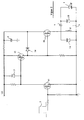
- FIG. 1 shows the circuit arrangement according to the invention for driving a laser diode (1).
- a storage capacitor (9) is set to a suitably high level via a charging circuit (5) Voltage (UB) - for example 50V to 100V - charged.
- a MOS-FET switch (10) switched through, which then the storage capacitor (9) with the LC resonant circuit (6) connects in which the laser diode (1) is arranged.
- the LC resonant circuit (6) - consisting of a capacitor (7) and a coil (8) as an inductive component - is preferably designed as a parallel resonant circuit, the laser diode (1) being connected in series the capacitor (7) is connected.
- the MOS-FET (10) is a Small power transistor.
- the gate of the MOS-FET switch (10) is with a Drive circuit (4) connected, which is designed so that it in turn in an advantageous manner Way of a digital logic circuit (e.g. in CMOS technology; the logic circuit itself is not shown) receives a trigger pulse (2).
- the control circuit (4) can can be controlled with a TTL signal of a logic circuit with low power, while the output of the drive circuit (4) is able to gate the MOS-FET (10) to be driven with a correspondingly high output.
- the pulse width of the TTL trigger pulse (2) is 50 nanoseconds, for example.
- the drain of the MOS-FETs (10) is with the Storage capacitor (9) connected while the source via the LC resonant circuit (6) the laser diode (1) is connected, the LC resonant circuit (6) with the laser diode (1) represents load to be switched.
- the fact that the laser diode (1) with the source and not with the drain is connected - as described in the introduction - the switching time of the MOS-FET (10) significantly shortened.
- the damped LC resonant circuit (6) in which the laser diode (1) is arranged leads to the fact that by the laser diode (1) when the Storage capacitor (9) only an almost semi-sinusoidal current pulse - cf. Figure 3B - flows.
- the damping is essentially achieved by a parallel to the LC resonant circuit (6) switched diode (14) causes the reverse polarity to the laser diode (1), while during negative half-wave, part of the discharge current flows through this diode (14) and thus the Oscillating circuit due to the drop in performance at the internal resistance of the diode (14) energy is withdrawn.
- the amplitude of the next positive half-wave is so low that none additional laser pulse is generated or in any case only one laser pulse with one negligible low performance. Without the LC resonant circuit (6) according to the invention an exponentially decreasing current would flow through the laser diode (1) would result in a correspondingly long laser pulse.
- an oppositely polarized diode (15) is connected in parallel to the laser diode (1).
- Both diodes (14, 15) - protective diode (15) and damping diode (14) - are preferably Schottky diodes, so that the charge can be reacted to quickly can.
- FIG. 2 shows the circuit arrangement with details of the control circuit (4).
- the storage capacitor (9) is charged to the operating voltage (UB) before a laser pulse.
- the positive edge of the TTL trigger signal (2) at the gate of the input MOS-FET (11) switches it through.
- This MOS-FET (11) is a self-locking N-channel MOS-FET.
- the gate is connected to ground via a resistor.
- the source is directly connected to ground.
- the drain of this MOS-FET (11) is connected via a resistor to the operating voltage (UB) and at the same time to the gate of a normally-off P-channel MOS-FET (12).
- the source of the P-channel MOS-FET (12) is connected to the operating voltage (UB).
- the drain of the P-channel MOS-FET (12) is connected to the gate of the N-channel MOS-FET (10), which ultimately the storage capacitor (9) with the LC resonant circuit (6) and the laser diode (1 ) connects.
- a Zener diode (13) connected, which when switching the input MOS-FETs (11) the voltage drop at the gate of the P-channel MOS-FET (12) compared to the Operating voltage limited to a maximum of Zener voltage.
- MOS-FET For the input MOS-FET (11), a MOS-FET is used, which is for low powers and currents is dimensioned and therefore advantageously with a TTL signal can be switched.
- the downstream P-channel MOS-FET (12) is for larger powers and currents dimensioned, because this MOS-FET (12) for a short time deliver correspondingly high switching currents for the downstream N-channel MOS FET (10) got to.
- the operating voltage to which the storage capacitor (9) is charged may vary Application and measuring situation can be changed and is therefore variable.
- Control circuit can be connected to a plurality of laser diodes via a multiplexer. So that will the control of several laser diodes realized with only one control circuit.
- the Several laser diodes are then preferably with their cathodes together with ground connected.
Landscapes
- Physics & Mathematics (AREA)
- Condensed Matter Physics & Semiconductors (AREA)
- General Physics & Mathematics (AREA)
- Electromagnetism (AREA)
- Optics & Photonics (AREA)
- Semiconductor Lasers (AREA)
- Lasers (AREA)
Abstract
Description
Mit der aus der DE 195 46 562 C1 bekannten Schaltungsanordnung sind jedoch nur Laserimpulse mit Impulsbreiten von einigen zehn Nanosekunden möglich. Dabei hat zum Beispiel eine Impulsbreite von 40 Nanosekunden zur Folge, daß Ziele, die weniger 12 Meter voneinander beabstandet sind, nicht mehr getrennt erkannt werden können.
- Figur 1
- eine schematische Darstellung der Schaltungsanordnung,
- Figur 2
- die Schaltungsanordnung mit den Details der MOS-FET-Ansteuerung,
- Figur 3A
- den zeitlichen Verlauf des Trigger-Impulses für die Ansteuerschaltung,
- Figur 3B
- den zeitlichen Verlauf des Stromimpulses durch die Laserdiode.
Der Speicherkondensator (9) ist jeweils vor einem Laserimpuls auf die Betriebsspannung (UB) aufgeladen. Die Ansteuerung des MOS-FETs (10), der den Speicherkondensator (9) über den LC-Schwingkreis (6) an die Laserdiode (1) durchschaltet, erfolgt über das sequentielle Einschalten zweier vorgeschalteter MOS-FETs (11, 12). Durch die positive Flanke des TTL-Triggersignals (2) am Gate des Eingangs-MOS-FETs (11) wird dieser durchgeschaltet. Bei diesem MOS-FET (11) handelt es sich um einen selbstsperrenden N-Kanal- MOS-FET. Das Gate ist über einen Widerstand mit Masse verbunden. Die Source ist direkt mit Masse verbunden. Der Drain dieses MOS-FETs (11) ist über einen Widerstand mit der Betriebsspannung (UB) und gleichzeitig mit dem Gate eines selbstsperrenden P-Kanal-MOS-FETs (12) verbunden. Die Source des P-Kanal- MOS-FETs (12) ist der Betriebsspannung (UB) verbunden. Der Drain des P-Kanal- MOS-FETs (12) ist mit dem Gate des N-Kanal- MOS-FET (10) verbunden, der letztendlich den Speicherkondensator (9) mit dem LC-Schwingkreis (6) und der Laserdiode (1) verbindet.
- 1)
- Laserdiode
- 2)
- Triggerimpuls
- UB)
- Betriebsspannung
- 3)
- Stromimpuls durch die Laserdiode
- 4)
- Ansteuerschaltung
- 5)
- Ladeschaltung
- 6)
- LC-Schwingkreis
- 7)
- Kondensator des Schwingkreises
- 8)
- Spule des Schwingkreises
- 9)
- Speicherkondensator
- 10)
- MOS-FET zum Durchschalten des Speicherkondensators an die Laserdiode
- 11)
- Eingangs-MOS-FET
- 12)
- P-Kanal-MOS-FET
- 13)
- Zenerdiode
- 14)
- Dämpfungsdiode für den Schwingkreis
- 15)
- Schutzdiode für die Laserdiode
- 16)
- Schutzdiode für das Gate des MOS-FETs ()
Claims (5)
- Schaltungsanordnung für mindestens eine Laserdiode (1) zur Erzeugung von kurzen Laserimpulsen mit einer Ansteuerschaltung (4) zur Ansteuerung eines MOS-FETs (10), welcher die Laserdiode (1) zur Erzeugung des Laserimpulses mit einem auf eine geeignet hohe Spannung aufgeladenen Speicherkondensator (9) verbindet, wobei der Entladestrom des Speicherkondensators (9) zumindest teilweise durch die Laserdiode (1) fließt,
dadurch gekennzeichnet, daß
die Laserdiode (1) in einem gedämpften LC-Schwingkreis (6) angeordnet ist. - Schaltungsanordnung nach Anspruch 1,
dadurch gekennzeichnet, daß
die Laserdiode (1) in einem LC-Parallelschwingkreis (6) angeordnet ist, wobei die Laserdiode (1) in Reihe zum Kondensator (7) des Schwingkreises (6) geschaltet ist. - Schaltungsanordnung nach einem der vorstehenden Ansprüche,
dadurch gekennzeichnet, daß
parallel zum LC-Schwingkreis (6) eine Diode (14) geschaltet ist, wobei die Polung dieser Diode (14) umgekehrt zur Laserdiode (1) ist. - Schaltungsanordnung nach Anspruch 3,
dadurch gekennzeichnet, daß
die Diode (14) eine Schottky-Diode ist. - Schaltungsanordnung für mindestens eine Laserdiode (1) zur Erzeugung von kurzen Laserimpulsen mit einer Ansteuerschaltung (4) zur Ansteuerung eines MOS-FETs (10), welcher die Laserdiode (1) zur Erzeugung des Laserimpulses mit einem auf eine geeignet hohe Spannung aufgeladenen Speicherkondensator (9) verbindet, wobei der Entladestrom des Speicherkondensators (9) zumindest teilweise durch die Laserdiode (1) fließt,
dadurch gekennzeichnet, daß
der Speicherkondensator (9) mit dem Drain des MOS-FETs (10) verbunden ist und die zu schaltende Last mit der Laserdiode (1) mit der Source des MOS-FETs (10) verbunden ist.
Applications Claiming Priority (2)
| Application Number | Priority Date | Filing Date | Title |
|---|---|---|---|
| DE10125465 | 2001-05-25 | ||
| DE10125465A DE10125465A1 (de) | 2001-05-25 | 2001-05-25 | Schaltungsanordnung für mindestens eine Laserdiode zur Erzeugung von kurzen Laserimpulsen |
Publications (3)
| Publication Number | Publication Date |
|---|---|
| EP1263140A2 true EP1263140A2 (de) | 2002-12-04 |
| EP1263140A3 EP1263140A3 (de) | 2006-07-19 |
| EP1263140B1 EP1263140B1 (de) | 2008-05-07 |
Family
ID=7686075
Family Applications (1)
| Application Number | Title | Priority Date | Filing Date |
|---|---|---|---|
| EP02010393A Expired - Lifetime EP1263140B1 (de) | 2001-05-25 | 2002-05-08 | Schaltungsanordnung zur Erzeugung von kurzen Laserimpulsen mit einer Laserdiode |
Country Status (3)
| Country | Link |
|---|---|
| EP (1) | EP1263140B1 (de) |
| AT (1) | ATE394833T1 (de) |
| DE (2) | DE10125465A1 (de) |
Cited By (1)
| Publication number | Priority date | Publication date | Assignee | Title |
|---|---|---|---|---|
| WO2007112823A3 (de) * | 2006-03-29 | 2008-06-05 | Ic Haus Gmbh | Schaltungsanordnung zum erzeugen schneller laserimpulse |
Families Citing this family (5)
| Publication number | Priority date | Publication date | Assignee | Title |
|---|---|---|---|---|
| DE102006036167B4 (de) * | 2006-08-01 | 2011-02-03 | Laserline Gesellschaft für Entwicklung und Vertrieb von Diodenlasern mbH | Schaltungsanordnung zum gepulsten Ansteuern einer Laserdiodenanordnung |
| CN111903019A (zh) | 2018-05-18 | 2020-11-06 | 海拉有限双合股份公司 | 用于激光二极管的驱动器电路以及具有这种驱动器电路和激光二极管的电路布置 |
| US11075502B2 (en) | 2019-08-29 | 2021-07-27 | Analog Devices, Inc. | Laser diode driver circuit techniques |
| US11621539B2 (en) | 2020-06-02 | 2023-04-04 | Analog Devices, Inc. | Multi-phase laser driver techniques |
| CN113092856B (zh) * | 2021-03-11 | 2022-01-04 | 广芯微电子(广州)股份有限公司 | 一种检测lc谐振频率的振荡器电路 |
Family Cites Families (9)
| Publication number | Priority date | Publication date | Assignee | Title |
|---|---|---|---|---|
| US3909745A (en) * | 1974-10-17 | 1975-09-30 | Hughes Aircraft Co | Laser transmitter system |
| US4400812A (en) * | 1981-06-15 | 1983-08-23 | Santa Barbara Research Center | Laser drive circuits |
| US5287372A (en) * | 1992-04-24 | 1994-02-15 | Hughes Aircraft Company | Quasi-resonant diode drive current source |
| US5394415A (en) * | 1992-12-03 | 1995-02-28 | Energy Compression Research Corporation | Method and apparatus for modulating optical energy using light activated semiconductor switches |
| CA2159842A1 (en) * | 1994-12-05 | 1996-06-06 | Joe A. Ortiz | Diode drive current source |
| DE19546562C1 (de) * | 1995-12-13 | 1997-04-03 | Leica Ag | Schaltungsanordnung zur Ansteuerung einer Impulsendstufe |
| US5852358A (en) * | 1996-12-11 | 1998-12-22 | The Texas A&M University System | Capactive power circuit |
| US5987045A (en) * | 1997-04-02 | 1999-11-16 | The United States Of America As Represented By The Secretary Of The Navy | High power narrow pulse laser diode circuit |
| US6067307A (en) * | 1998-06-12 | 2000-05-23 | Lucent Technologies Inc. | Vertical cavity surface emitting laser driving circuit |
-
2001
- 2001-05-25 DE DE10125465A patent/DE10125465A1/de not_active Withdrawn
-
2002
- 2002-05-08 EP EP02010393A patent/EP1263140B1/de not_active Expired - Lifetime
- 2002-05-08 DE DE50212204T patent/DE50212204D1/de not_active Expired - Lifetime
- 2002-05-08 AT AT02010393T patent/ATE394833T1/de not_active IP Right Cessation
Cited By (1)
| Publication number | Priority date | Publication date | Assignee | Title |
|---|---|---|---|---|
| WO2007112823A3 (de) * | 2006-03-29 | 2008-06-05 | Ic Haus Gmbh | Schaltungsanordnung zum erzeugen schneller laserimpulse |
Also Published As
| Publication number | Publication date |
|---|---|
| EP1263140A3 (de) | 2006-07-19 |
| ATE394833T1 (de) | 2008-05-15 |
| DE10125465A1 (de) | 2002-11-28 |
| EP1263140B1 (de) | 2008-05-07 |
| DE50212204D1 (de) | 2008-06-19 |
Similar Documents
| Publication | Publication Date | Title |
|---|---|---|
| DE10301655B4 (de) | Steuerschaltung für eine Leistungshalbleitervorrichtung | |
| DE2834110C2 (de) | ||
| DE69329791T2 (de) | Schaltkreis zur abschaltung einer induktiven last | |
| DE2659207B2 (de) | In einem integrierten MOSFET-Schaltkreis ausgebildete Verzögerungsstufe | |
| DE69500086T2 (de) | Schaltungsanordnung zur Spannungsbegrenzung mit Hysteresiskomparator | |
| DE3318537A1 (de) | Schnell arbeitender analog-digital-konverter | |
| DE4413546A1 (de) | Gleichstrom-Steuerschaltung | |
| DE69216141T2 (de) | Variable Pegeltreiberschaltung für periodische Ansteuerung einer kapazitiven Last | |
| DE2306607A1 (de) | Schaltungsanordnung zur ansteuerung einer induktiven last | |
| EP1263140B1 (de) | Schaltungsanordnung zur Erzeugung von kurzen Laserimpulsen mit einer Laserdiode | |
| DE3904910C2 (de) | ||
| DE102005027442B4 (de) | Schaltungsanordnung zum Schalten einer Last | |
| DE102016213200B4 (de) | Schaltungsanordnung zum Ansteuern einer induktiven Last | |
| EP2251979A1 (de) | Verfahren und Treiberschaltung zum Treiben eines Halbleiterleistungsschalters | |
| EP3023832B1 (de) | Pockelszellen-Treiberschaltung mit Induktivitäten | |
| DE10064123A1 (de) | Schaltungsanordnung zur Ansteuerung eines Halbleiterschaltelements | |
| EP0876699B1 (de) | Strombegrenzungsschaltung | |
| DE2135858C3 (de) | Transistorschalteinrichtung zum Schalten eines induktiven Gleichstromkreises | |
| DE102010004488B3 (de) | Pegelwandlerschaltung | |
| DE3536447C2 (de) | Kurzschluß- und überlastfeste Transistorausgangsstufe | |
| DE102007050049A1 (de) | Schalteranordnung mit einer Pegelschiebereinrichtung | |
| DE10305361B4 (de) | Elektronischer Hochfrequenz-Schalter | |
| DE2613227C2 (de) | Schaltungsanordnung zur Auslösung eines drehzahlabhängigen Schaltvorganges | |
| DE10136320B4 (de) | Anordnung und Verfahren zum Umschalten von Transistoren | |
| DE1182296B (de) | Schaltungsanordnung zur Realisierung logischer Funktionen |
Legal Events
| Date | Code | Title | Description |
|---|---|---|---|
| PUAI | Public reference made under article 153(3) epc to a published international application that has entered the european phase |
Free format text: ORIGINAL CODE: 0009012 |
|
| AK | Designated contracting states |
Kind code of ref document: A2 Designated state(s): AT BE CH CY DE DK ES FI FR GB GR IE IT LI LU MC NL PT SE TR |
|
| AX | Request for extension of the european patent |
Free format text: AL;LT;LV;MK;RO;SI |
|
| RAP1 | Party data changed (applicant data changed or rights of an application transferred) |
Owner name: HELLA KGAA HUECK & CO. |
|
| PUAL | Search report despatched |
Free format text: ORIGINAL CODE: 0009013 |
|
| AK | Designated contracting states |
Kind code of ref document: A3 Designated state(s): AT BE CH CY DE DK ES FI FR GB GR IE IT LI LU MC NL PT SE TR |
|
| AX | Request for extension of the european patent |
Extension state: AL LT LV MK RO SI |
|
| RIC1 | Information provided on ipc code assigned before grant |
Ipc: H03K 17/0416 20060101AFI20020909BHEP Ipc: H01S 5/042 20060101ALI20060609BHEP Ipc: H03K 17/687 20060101ALI20060609BHEP |
|
| 17P | Request for examination filed |
Effective date: 20061218 |
|
| 17Q | First examination report despatched |
Effective date: 20070213 |
|
| AKX | Designation fees paid |
Designated state(s): AT BE CH CY DE DK ES FI FR GB GR IE IT LI LU MC NL PT SE TR |
|
| GRAP | Despatch of communication of intention to grant a patent |
Free format text: ORIGINAL CODE: EPIDOSNIGR1 |
|
| GRAS | Grant fee paid |
Free format text: ORIGINAL CODE: EPIDOSNIGR3 |
|
| GRAA | (expected) grant |
Free format text: ORIGINAL CODE: 0009210 |
|
| AK | Designated contracting states |
Kind code of ref document: B1 Designated state(s): AT BE CH CY DE DK ES FI FR GB GR IE IT LI LU MC NL PT SE TR |
|
| REG | Reference to a national code |
Ref country code: GB Ref legal event code: FG4D Free format text: NOT ENGLISH |
|
| REG | Reference to a national code |
Ref country code: CH Ref legal event code: EP |
|
| REG | Reference to a national code |
Ref country code: IE Ref legal event code: FG4D Free format text: LANGUAGE OF EP DOCUMENT: GERMAN |
|
| REF | Corresponds to: |
Ref document number: 50212204 Country of ref document: DE Date of ref document: 20080619 Kind code of ref document: P |
|
| PG25 | Lapsed in a contracting state [announced via postgrant information from national office to epo] |
Ref country code: NL Free format text: LAPSE BECAUSE OF FAILURE TO SUBMIT A TRANSLATION OF THE DESCRIPTION OR TO PAY THE FEE WITHIN THE PRESCRIBED TIME-LIMIT Effective date: 20080507 Ref country code: FI Free format text: LAPSE BECAUSE OF FAILURE TO SUBMIT A TRANSLATION OF THE DESCRIPTION OR TO PAY THE FEE WITHIN THE PRESCRIBED TIME-LIMIT Effective date: 20080507 Ref country code: ES Free format text: LAPSE BECAUSE OF FAILURE TO SUBMIT A TRANSLATION OF THE DESCRIPTION OR TO PAY THE FEE WITHIN THE PRESCRIBED TIME-LIMIT Effective date: 20080818 |
|
| NLV1 | Nl: lapsed or annulled due to failure to fulfill the requirements of art. 29p and 29m of the patents act | ||
| BERE | Be: lapsed |
Owner name: HELLA KGAA HUECK & CO. Effective date: 20080531 |
|
| REG | Reference to a national code |
Ref country code: IE Ref legal event code: FD4D |
|
| PG25 | Lapsed in a contracting state [announced via postgrant information from national office to epo] |
Ref country code: MC Free format text: LAPSE BECAUSE OF NON-PAYMENT OF DUE FEES Effective date: 20080531 |
|
| REG | Reference to a national code |
Ref country code: CH Ref legal event code: PL |
|
| PG25 | Lapsed in a contracting state [announced via postgrant information from national office to epo] |
Ref country code: LI Free format text: LAPSE BECAUSE OF NON-PAYMENT OF DUE FEES Effective date: 20080531 Ref country code: CH Free format text: LAPSE BECAUSE OF NON-PAYMENT OF DUE FEES Effective date: 20080531 Ref country code: IE Free format text: LAPSE BECAUSE OF FAILURE TO SUBMIT A TRANSLATION OF THE DESCRIPTION OR TO PAY THE FEE WITHIN THE PRESCRIBED TIME-LIMIT Effective date: 20080507 Ref country code: SE Free format text: LAPSE BECAUSE OF FAILURE TO SUBMIT A TRANSLATION OF THE DESCRIPTION OR TO PAY THE FEE WITHIN THE PRESCRIBED TIME-LIMIT Effective date: 20080807 Ref country code: PT Free format text: LAPSE BECAUSE OF FAILURE TO SUBMIT A TRANSLATION OF THE DESCRIPTION OR TO PAY THE FEE WITHIN THE PRESCRIBED TIME-LIMIT Effective date: 20081007 Ref country code: DK Free format text: LAPSE BECAUSE OF FAILURE TO SUBMIT A TRANSLATION OF THE DESCRIPTION OR TO PAY THE FEE WITHIN THE PRESCRIBED TIME-LIMIT Effective date: 20080507 |
|
| PLBE | No opposition filed within time limit |
Free format text: ORIGINAL CODE: 0009261 |
|
| STAA | Information on the status of an ep patent application or granted ep patent |
Free format text: STATUS: NO OPPOSITION FILED WITHIN TIME LIMIT |
|
| PG25 | Lapsed in a contracting state [announced via postgrant information from national office to epo] |
Ref country code: BE Free format text: LAPSE BECAUSE OF NON-PAYMENT OF DUE FEES Effective date: 20080531 |
|
| 26N | No opposition filed |
Effective date: 20090210 |
|
| GBPC | Gb: european patent ceased through non-payment of renewal fee |
Effective date: 20080807 |
|
| PG25 | Lapsed in a contracting state [announced via postgrant information from national office to epo] |
Ref country code: AT Free format text: LAPSE BECAUSE OF NON-PAYMENT OF DUE FEES Effective date: 20080508 |
|
| PGFP | Annual fee paid to national office [announced via postgrant information from national office to epo] |
Ref country code: FR Payment date: 20090515 Year of fee payment: 8 Ref country code: IT Payment date: 20090518 Year of fee payment: 8 |
|
| PG25 | Lapsed in a contracting state [announced via postgrant information from national office to epo] |
Ref country code: GB Free format text: LAPSE BECAUSE OF NON-PAYMENT OF DUE FEES Effective date: 20080807 |
|
| PG25 | Lapsed in a contracting state [announced via postgrant information from national office to epo] |
Ref country code: CY Free format text: LAPSE BECAUSE OF FAILURE TO SUBMIT A TRANSLATION OF THE DESCRIPTION OR TO PAY THE FEE WITHIN THE PRESCRIBED TIME-LIMIT Effective date: 20080507 Ref country code: LU Free format text: LAPSE BECAUSE OF NON-PAYMENT OF DUE FEES Effective date: 20080508 |
|
| PG25 | Lapsed in a contracting state [announced via postgrant information from national office to epo] |
Ref country code: TR Free format text: LAPSE BECAUSE OF FAILURE TO SUBMIT A TRANSLATION OF THE DESCRIPTION OR TO PAY THE FEE WITHIN THE PRESCRIBED TIME-LIMIT Effective date: 20080507 |
|
| PG25 | Lapsed in a contracting state [announced via postgrant information from national office to epo] |
Ref country code: GR Free format text: LAPSE BECAUSE OF FAILURE TO SUBMIT A TRANSLATION OF THE DESCRIPTION OR TO PAY THE FEE WITHIN THE PRESCRIBED TIME-LIMIT Effective date: 20080808 |
|
| REG | Reference to a national code |
Ref country code: FR Ref legal event code: ST Effective date: 20110131 |
|
| PG25 | Lapsed in a contracting state [announced via postgrant information from national office to epo] |
Ref country code: IT Free format text: LAPSE BECAUSE OF NON-PAYMENT OF DUE FEES Effective date: 20100508 |
|
| PG25 | Lapsed in a contracting state [announced via postgrant information from national office to epo] |
Ref country code: FR Free format text: LAPSE BECAUSE OF NON-PAYMENT OF DUE FEES Effective date: 20100531 |
|
| PGFP | Annual fee paid to national office [announced via postgrant information from national office to epo] |
Ref country code: DE Payment date: 20130515 Year of fee payment: 12 |
|
| REG | Reference to a national code |
Ref country code: DE Ref legal event code: R119 Ref document number: 50212204 Country of ref document: DE |
|
| REG | Reference to a national code |
Ref country code: DE Ref legal event code: R119 Ref document number: 50212204 Country of ref document: DE Effective date: 20141202 |
|
| PG25 | Lapsed in a contracting state [announced via postgrant information from national office to epo] |
Ref country code: DE Free format text: LAPSE BECAUSE OF NON-PAYMENT OF DUE FEES Effective date: 20141202 |