EP1263129A1 - DC feedback control circuit - Google Patents
DC feedback control circuit Download PDFInfo
- Publication number
- EP1263129A1 EP1263129A1 EP01304467A EP01304467A EP1263129A1 EP 1263129 A1 EP1263129 A1 EP 1263129A1 EP 01304467 A EP01304467 A EP 01304467A EP 01304467 A EP01304467 A EP 01304467A EP 1263129 A1 EP1263129 A1 EP 1263129A1
- Authority
- EP
- European Patent Office
- Prior art keywords
- transistor
- coupled
- current
- circuit
- electrode
- Prior art date
- Legal status (The legal status is an assumption and is not a legal conclusion. Google has not performed a legal analysis and makes no representation as to the accuracy of the status listed.)
- Withdrawn
Links
- 230000001419 dependent effect Effects 0.000 claims abstract description 4
- 238000000034 method Methods 0.000 claims description 6
- 230000008878 coupling Effects 0.000 claims description 4
- 238000010168 coupling process Methods 0.000 claims description 4
- 238000005859 coupling reaction Methods 0.000 claims description 4
- 230000008859 change Effects 0.000 description 5
- 239000003990 capacitor Substances 0.000 description 3
- 238000010586 diagram Methods 0.000 description 1
- 230000006872 improvement Effects 0.000 description 1
- 230000004048 modification Effects 0.000 description 1
- 238000012986 modification Methods 0.000 description 1
- 230000009467 reduction Effects 0.000 description 1
- 230000004044 response Effects 0.000 description 1
- 230000007704 transition Effects 0.000 description 1
Images
Classifications
-
- H—ELECTRICITY
- H03—ELECTRONIC CIRCUITRY
- H03F—AMPLIFIERS
- H03F3/00—Amplifiers with only discharge tubes or only semiconductor devices as amplifying elements
- H03F3/34—DC amplifiers in which all stages are DC-coupled
- H03F3/343—DC amplifiers in which all stages are DC-coupled with semiconductor devices only
- H03F3/3432—DC amplifiers in which all stages are DC-coupled with semiconductor devices only with bipolar transistors
-
- H—ELECTRICITY
- H03—ELECTRONIC CIRCUITRY
- H03F—AMPLIFIERS
- H03F1/00—Details of amplifiers with only discharge tubes, only semiconductor devices or only unspecified devices as amplifying elements
- H03F1/30—Modifications of amplifiers to reduce influence of variations of temperature or supply voltage or other physical parameters
- H03F1/302—Modifications of amplifiers to reduce influence of variations of temperature or supply voltage or other physical parameters in bipolar transistor amplifiers
-
- G—PHYSICS
- G05—CONTROLLING; REGULATING
- G05F—SYSTEMS FOR REGULATING ELECTRIC OR MAGNETIC VARIABLES
- G05F3/00—Non-retroactive systems for regulating electric variables by using an uncontrolled element, or an uncontrolled combination of elements, such element or such combination having self-regulating properties
- G05F3/02—Regulating voltage or current
- G05F3/08—Regulating voltage or current wherein the variable is DC
- G05F3/10—Regulating voltage or current wherein the variable is DC using uncontrolled devices with non-linear characteristics
- G05F3/16—Regulating voltage or current wherein the variable is DC using uncontrolled devices with non-linear characteristics being semiconductor devices
- G05F3/20—Regulating voltage or current wherein the variable is DC using uncontrolled devices with non-linear characteristics being semiconductor devices using diode- transistor combinations
- G05F3/26—Current mirrors
- G05F3/265—Current mirrors using bipolar transistors only
Definitions
- This invention relates, in general, to a DC feedback control circuit and more particularly, though not exclusively, to such a circuit used for compensating for a DC level shift in a circuit using a resistor as a current source, for example a high frequency amplifier.
- the present invention provides a DC feedback control circuit for controlling the DC level of a circuit element having a current electrode of a transistor coupled to the signal output terminal, the DC feedback control circuit comprising an input terminal for coupling to a signal output terminal of the circuit element, a filter coupled to the input terminal, a comparator coupled to the filter and to a reference voltage input for comparing a DC voltage level at the signal output terminal with a reference voltage, a current mirror circuit coupled to the comparator and having an output terminal for coupling to a current electrode of the transistor of the circuit element, wherein the current mirror circuit mirrors the current output of the comparator to the output terminal.
- a high frequency amplifier comprising an amplifier circuit having an input, at least one transistor having a first current electrode coupled to a first voltage supply rail and a second current electrode coupled to a second voltage supply rail, and a signal output terminal coupled to the first current electrode of the at least one transistor, and a DC feedback control circuit as described above wherein the input terminal is coupled to the signal output terminal and the output terminal is coupled to the second current electrode of the at least one transistor.
- the invention provides a method of compensating for a DC voltage level shift in a circuit using a resistor as a current source and a transistor as a high speed switching device, the method comprising the steps of determining a DC voltage level at an output of the circuit, comparing the DC voltage level with a reference voltage, mirroring a current dependent on the comparison of the DC voltage level with the reference voltage, and applying the mirrored current to the transistor at an emitter thereof to maintain a substantially constant bias current therethrough.
- a transimpedance amplifier 12 has a signal input 10 coupled to a base electrode of a first transistor 14. An emitter electrode of the first transistor 14 of the transimpedance amplifier 12 is coupled to a resistor 16 and a collector electrode of the first transistor 14 of the transimpedance amplifier 12 is coupled to a resistor 18.
- a base electrode of a second transistor 20 of the transimpedance amplifier 12 is coupled to the collector electrode of the first transistor 14 of transimpedance amplifier 12.
- An emitter electrode of the second transistor 20 of the transimpedance amplifier 12 is coupled to a resistor 22 and a collector electrode of the second transistor 20 of the transimpedance amplifier 12 is coupled to a resistor 24.
- Both the resistor 18 and the resistor 24 are coupled to a relative supply voltage rail 56.
- Both the resistor 16 and the resistor 22 are coupled to a relative ground voltage rail 58.
- An additional resistor 26 is coupled between the emitter electrode of the second transistor 20 of the transimpedance amplifier 12 and the signal input 10.
- the collector electrode of the second transistor 20 of the transimpedance amplifier 12 is coupled to a signal output 28.
- a collector electrode of the second transistor 40 of the differential pair 36 is connected to the relative supply voltage rail 56.
- the voltage on the signal output 28 is thus filtered by filter 30 to remove any AC components and provide a DC level, which is then compared by differential pair 36 to the reference voltage 41.
- a collector electrode of the first transistor 38 of the differential pair 36 is coupled to a collector electrode of a first transistor 46 of a first current mirror 44.
- a base electrode of the first transistor 46 of the first current mirror 44 is coupled to a base electrode of a second transistor 48 of the first current mirror 44.
- Emitter electrodes of both the first transistor 46 and the second transistor 48 of the first current mirror are coupled to the relative supply voltage rail 56. Also, the base electrode and the collector electrode of the first transistor 46 of the first current mirror 44 are coupled together.
- the first current mirror 44 is connected to a second current mirror 50. More specifically, a collector electrode of the second transistor 48 of the first current mirror 44 is connected to a collector electrode of a first transistor 52 of a second current mirror 50. A base electrode of the first transistor 52 of the second current mirror 50 is coupled to a base electrode of a second transistor 54 of the second current mirror 50. Emitter electrodes of both the first transistor 52 and the second transistor 54 of the second current mirror 50 are coupled to the relative ground voltage rail 58. Also, the base electrode and the collector electrode of the first transistor 52 of the second current mirror 50 are coupled together.
- the second current mirror 50 is connected to the transimpedance amplifier 12. More specifically, a collector electrode of the second transistor 54 of the second current mirror 50 is coupled between the emitter electrode of the second transistor 20 and resistor 22 of the transimpedance amplifier 12.
- a signal is applied to the signal input 10 and amplified by the transimpedance amplifier 12.
- An output signal is filtered by the filter 30.
- the capacitor 34 functions to remove any a.c. aspect present in the output signal, so that the d.c. level of the output signal is applied to the differential pair 36.
- the differential pair 36 functions as a comparator to compare the DC level of the output signal with the reference voltage 41, which determines a level of feedback.
- a current determined by the level of feedback is passed from the collector electrode of the first transistor 38 of the differential pair 36 to the collector electrode of the first transistor 46 of the first current mirror 44, where it is mirrored by second transistor 48 and applied to second current mirror 50.
- the current is fed back through the second current mirror 50 and applied to the emitter electrode of the second transistor 20 of the transimpedance amplifier 12 to maintain a near constant bias current flowing through the transistor.
- the characteristics of the feedback current can be adjusted to feedback any proportion of the DC voltage change required, dependant on the level of the reference voltage 41.
- a near constant bias current flowing through the second transistor 20 of transimpedance amplifier 12 is achieved by the present nvention, even if the DC voltage of second transistor 20 changes.
- a change in bias current which can impair maximum switching-speed of the :ransimpedance amplifier 12 is avoided.
- the above technique is particularly useful in high frequency amplifiers , such as transimpedance amplifiers, where the bias voltages are strongly dependent on signal amplitude.
Landscapes
- Engineering & Computer Science (AREA)
- Power Engineering (AREA)
- Amplifiers (AREA)
Abstract
A DC feedback control circuit for compensating for a DC voltage level shift
in a transimpedance amplifier circuit (12) having a transistor (20) as a high
speed switching device. The DC feedback control circuit includes a filter
(30) for determining a DC voltage level at an output of the amplifier circuit
(12) and a differential pair (36) of transistors for comparing the DC voltage
level with a reference voltage (41). A pair of current mirrors (44 and 50)
mirror a current dependent on the comparison of the DC voltage level with
the reference voltage and apply the mirrored current to an emitter of the
transistor (20) so as to maintain a substantially constant bias current
through the switching transistor (20).
Description
- This invention relates, in general, to a DC feedback control circuit and more particularly, though not exclusively, to such a circuit used for compensating for a DC level shift in a circuit using a resistor as a current source, for example a high frequency amplifier.
- In integrated circuits, a DC voltage applied to a particular component can often change as a result of changes in temperature, supply voltage, or even in response to a data signal being applied to the circuit. When a transistor is being used as an amplifier, to achieve the maximum switching speed for that amplifier the bias current of the switching transistor should be maintained at or near IC for peak FT where FT is the transition frequency and IC is the current flowing through the collector of the transistor. It will thus be apparent that if the DC voltage of the transistor changes, this will often cause a change in the bias current, leading to a reduction in the high speed performance of the circuit.
- It is therefore an object of the present invention to provide a DC feedback control circuit which can overcome, or at least alleviate the problems caused by a fluctuating DC level.
- Accordingly, in a first aspect, the present invention provides a DC feedback control circuit for controlling the DC level of a circuit element having a current electrode of a transistor coupled to the signal output terminal, the DC feedback control circuit comprising an input terminal for coupling to a signal output terminal of the circuit element, a filter coupled to the input terminal, a comparator coupled to the filter and to a reference voltage input for comparing a DC voltage level at the signal output terminal with a reference voltage, a current mirror circuit coupled to the comparator and having an output terminal for coupling to a current electrode of the transistor of the circuit element, wherein the current mirror circuit mirrors the current output of the comparator to the output terminal.
- According to a second aspect of the present invention, there is provided a high frequency amplifier comprising an amplifier circuit having an input, at least one transistor having a first current electrode coupled to a first voltage supply rail and a second current electrode coupled to a second voltage supply rail, and a signal output terminal coupled to the first current electrode of the at least one transistor, and a DC feedback control circuit as described above wherein the input terminal is coupled to the signal output terminal and the output terminal is coupled to the second current electrode of the at least one transistor.
- In a third aspect, the invention provides a method of compensating for a DC voltage level shift in a circuit using a resistor as a current source and a transistor as a high speed switching device, the method comprising the steps of determining a DC voltage level at an output of the circuit, comparing the DC voltage level with a reference voltage, mirroring a current dependent on the comparison of the DC voltage level with the reference voltage, and applying the mirrored current to the transistor at an emitter thereof to maintain a substantially constant bias current therethrough.
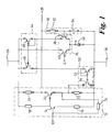
- An embodiment of the present invention will now be described, by way of example, with reference to the accompanying drawing which shows a circuit diagram of a DC feedback control circuit according to one embodiment of the present invention used to control the DC level of a transimpedance amplifier.
- Thus, in FIG.1 a
transimpedance amplifier 12 has asignal input 10 coupled to a base electrode of afirst transistor 14. An emitter electrode of thefirst transistor 14 of thetransimpedance amplifier 12 is coupled to aresistor 16 and a collector electrode of thefirst transistor 14 of thetransimpedance amplifier 12 is coupled to aresistor 18. - A base electrode of a
second transistor 20 of thetransimpedance amplifier 12 is coupled to the collector electrode of thefirst transistor 14 oftransimpedance amplifier 12. An emitter electrode of thesecond transistor 20 of thetransimpedance amplifier 12 is coupled to aresistor 22 and a collector electrode of thesecond transistor 20 of thetransimpedance amplifier 12 is coupled to aresistor 24. Both theresistor 18 and theresistor 24 are coupled to a relativesupply voltage rail 56. Both theresistor 16 and theresistor 22 are coupled to a relativeground voltage rail 58. Anadditional resistor 26 is coupled between the emitter electrode of thesecond transistor 20 of thetransimpedance amplifier 12 and thesignal input 10. Furthermore, the collector electrode of thesecond transistor 20 of thetransimpedance amplifier 12 is coupled to a signal output 28. - The DC feedback control circuit includes a filter 30 coupled to the signal output 28. The filter 30 comprises a
resistor 32 and acapacitor 34 connected in series. Adifferential pair 36 oftransistors resistor 32 and thecapacitor 34. More specifically, a base electrode of afirst transistor 38 of thedifferential pair 36 is connected to the filter 30. An emitter electrode of the first :ransistor 38 of thedifferential pair 36 and an emitter electrode of thesecond transistor 40 of thedifferential pair 36 are symmetrically connected to acurrent source 42 which, in turn, is connected to a relativeground voltage rail 58. A base electrode of thesecond transistor 40 of thedifferential pair 36 is coupled to areference voltage 41. A collector electrode of thesecond transistor 40 of thedifferential pair 36 is connected to the relativesupply voltage rail 56. The voltage on the signal output 28 is thus filtered by filter 30 to remove any AC components and provide a DC level, which is then compared bydifferential pair 36 to thereference voltage 41. - A collector electrode of the
first transistor 38 of thedifferential pair 36 is coupled to a collector electrode of afirst transistor 46 of a firstcurrent mirror 44. A base electrode of thefirst transistor 46 of the firstcurrent mirror 44 is coupled to a base electrode of asecond transistor 48 of the firstcurrent mirror 44. Emitter electrodes of both thefirst transistor 46 and thesecond transistor 48 of the first current mirror are coupled to the relativesupply voltage rail 56. Also, the base electrode and the collector electrode of thefirst transistor 46 of the firstcurrent mirror 44 are coupled together. - The first
current mirror 44 is connected to a secondcurrent mirror 50.
More specifically, a collector electrode of thesecond transistor 48 of the firstcurrent mirror 44 is connected to a collector electrode of afirst transistor 52 of a secondcurrent mirror 50. A base electrode of thefirst transistor 52 of the secondcurrent mirror 50 is coupled to a base electrode of asecond transistor 54 of the secondcurrent mirror 50. Emitter electrodes of both thefirst transistor 52 and thesecond transistor 54 of the secondcurrent mirror 50 are coupled to the relativeground voltage rail 58. Also, the base electrode and the collector electrode of thefirst transistor 52 of the secondcurrent mirror 50 are coupled together. - The second
current mirror 50 is connected to thetransimpedance amplifier 12. More specifically, a collector electrode of thesecond transistor 54 of the secondcurrent mirror 50 is coupled between the emitter electrode of thesecond transistor 20 andresistor 22 of thetransimpedance amplifier 12. - In operation, a signal is applied to the
signal input 10 and amplified by thetransimpedance amplifier 12. An output signal is filtered by the filter 30. Thecapacitor 34 functions to remove any a.c. aspect present in the output signal, so that the d.c. level of the output signal is applied to thedifferential pair 36. Thedifferential pair 36 functions as a comparator to compare the DC level of the output signal with thereference voltage 41, which determines a level of feedback. A current determined by the level of feedback is passed from the collector electrode of thefirst transistor 38 of thedifferential pair 36 to the collector electrode of thefirst transistor 46 of the firstcurrent mirror 44, where it is mirrored bysecond transistor 48 and applied to secondcurrent mirror 50. The current is fed back through the secondcurrent mirror 50 and applied to the emitter electrode of thesecond transistor 20 of thetransimpedance amplifier 12 to maintain a near constant bias current flowing through the transistor. - The characteristics of the feedback current can be adjusted to feedback any proportion of the DC voltage change required, dependant on the level of the
reference voltage 41. - Advantageously, a near constant bias current flowing through the
second transistor 20 oftransimpedance amplifier 12 is achieved by the present nvention, even if the DC voltage ofsecond transistor 20 changes. Thus, a change in bias current which can impair maximum switching-speed of the :ransimpedance amplifier 12 is avoided. The above technique is particularly useful in high frequency amplifiers , such as transimpedance amplifiers, where the bias voltages are strongly dependent on signal amplitude. - Whilst the invention has been described above in respect of a particular embodiment, namely a transimpedance amplifier, it will be appreciated that the present invention is applicable to any integrated circuit in which the DC voltage applied is susceptible to change. Furthermore, it will be appreciated that the above description has been given by way of example only and that a person skilled in the art can make modifications and improvement without departing from the scope of the present invention.
Claims (11)
1. A DC feedback control circuit for controlling the DC level of a circuit
element having a current electrode of a transistor coupled to the signal
output terminal, the DC feedback control circuit comprising:
an input terminal for coupling to a signal output terminal of the circuit
element;
a filter coupled to the input terminal;
a comparator coupled to the filter and to a reference voltage input for
comparing a DC voltage level at the signal output terminal with a reference
voltage;
a current mirror circuit coupled to the comparator and having an
output terminal for coupling to a current electrode of the transistor of the
circuit element, wherein the current mirror circuit mirrors the current output
of the comparator to the output terminal.
2. A DC feedback control circuit according to claim 1, wherein the
comparator comprises a differential pair of transistors.
3. A DC feedback control circuit according to either claim 1 or claim 2,
wherein the current mirror circuit comprises a pair of current mirrors,
wherein a first current mirror of the pair of current mirrors has an input
coupled to an output of the comparator and an output coupled to an input
of a second current mirror of the pair of current mirrors, an output of the
second current mirror being coupled to the output terminal.
4. A DC feedback control circuit according to any preceding claim,
wherein the filter comprises an RC filter.
5. A high frequency amplifier comprising an amplifier circuit having an
input, at least one transistor having a first current electrode coupled to a
first voltage supply rail and a second current electrode coupled to a second
voltage supply rail, and a signal output terminal coupled to the first current
electrode of the at least one transistor, and a DC feedback control circuit
according to any preceding claim wherein the input terminal is coupled to
the signal output terminal and the output terminal is coupled to the second
current electrode of the at least one transistor.
5. A high frequency amplifier according to claim 4, wherein the amplifier
circuit is a transimpedance amplifier circuit.
6. A high frequency amplifier according to claim 5, wherein the first
current electrode of the at least one transistor is coupled to the first voltage
supply rail via a first resistor.
7. A high frequency amplifier according to either claim 5 or claim 6,
wherein the second current electrode of the at least one transistor is
coupled to the second voltage supply rail via a second resistor.
8. A high frequency amplifier according to any one of claims 5 to 7,
further comprising a second transistor having a first current electrode
coupled to the first voltage supply rail via a third resistor and to the base
electrode of the at least one transistor, a second current electrode coupled
to the second voltage supply rail via a fourth resistor, and a fifth resistor
coupled between the second current electrode of the at least one transistor
and a base electrode of the second transistor.
9. A method of compensating for a DC voltage level shift in a circuit
using a resistor as a current source and a transistor as a high speed
switching device, the method comprising the steps of:
determining a DC voltage level at an output of the circuit;
comparing the DC voltage level with a reference voltage;
mirroring a current dependent on the comparison of the DC voltage
level with the reference voltage; and
applying the mirrored current to the transistor at an emitter thereof to
maintain a substantially constant bias current therethrough.
10. A method of compensating for a DC voltage level shift according to
claim 9, wherein the circuit is a transimpedance amplifier.
Priority Applications (2)
| Application Number | Priority Date | Filing Date | Title |
|---|---|---|---|
| EP01304467A EP1263129A1 (en) | 2001-05-21 | 2001-05-21 | DC feedback control circuit |
| US10/151,433 US6741134B2 (en) | 2001-05-21 | 2002-05-21 | DC feedback control circuit |
Applications Claiming Priority (1)
| Application Number | Priority Date | Filing Date | Title |
|---|---|---|---|
| EP01304467A EP1263129A1 (en) | 2001-05-21 | 2001-05-21 | DC feedback control circuit |
Publications (1)
| Publication Number | Publication Date |
|---|---|
| EP1263129A1 true EP1263129A1 (en) | 2002-12-04 |
Family
ID=8181973
Family Applications (1)
| Application Number | Title | Priority Date | Filing Date |
|---|---|---|---|
| EP01304467A Withdrawn EP1263129A1 (en) | 2001-05-21 | 2001-05-21 | DC feedback control circuit |
Country Status (2)
| Country | Link |
|---|---|
| US (1) | US6741134B2 (en) |
| EP (1) | EP1263129A1 (en) |
Families Citing this family (3)
| Publication number | Priority date | Publication date | Assignee | Title |
|---|---|---|---|---|
| US7042295B2 (en) * | 2004-03-31 | 2006-05-09 | Cornell Research Foundation, Inc. | Low-voltage, low-power transimpedance amplifier architecture |
| US20070262766A1 (en) * | 2006-05-11 | 2007-11-15 | Sige Semiconductor Inc. | Current mirror for high frequency monolithic integrated circuits |
| US8471639B2 (en) * | 2010-07-06 | 2013-06-25 | Luxtera Inc. | Method and system for a feedback transimpedance amplifier with sub-40khz low-frequency cutoff |
Citations (4)
| Publication number | Priority date | Publication date | Assignee | Title |
|---|---|---|---|---|
| US4451799A (en) * | 1980-07-30 | 1984-05-29 | Matsushita Electric Industrial Co., Ltd. | B-Class complementary circuit |
| JPH0766642A (en) * | 1993-08-27 | 1995-03-10 | Fujitsu Ltd | Bias supply circuit and semiconductor integrated circuit |
| JPH09321555A (en) * | 1996-05-28 | 1997-12-12 | Oki Electric Ind Co Ltd | Semiconductor integrated circuit differential amplifier |
| US5714909A (en) * | 1996-06-14 | 1998-02-03 | Sigmatel, Inc. | Transimpedance amplifier and method for constructing same |
Family Cites Families (3)
| Publication number | Priority date | Publication date | Assignee | Title |
|---|---|---|---|---|
| US4420724A (en) * | 1982-05-17 | 1983-12-13 | Bell Telephone Laboratories, Incorporated | FET Amplifier with wide dynamic range |
| US5216386A (en) * | 1991-12-20 | 1993-06-01 | Honeywell Inc. | Transimpedance amplifier |
| FR2700083B1 (en) * | 1992-12-30 | 1995-02-24 | Gerard Perrot | Stable distortion amplifier for audio signals. |
-
2001
- 2001-05-21 EP EP01304467A patent/EP1263129A1/en not_active Withdrawn
-
2002
- 2002-05-21 US US10/151,433 patent/US6741134B2/en not_active Expired - Fee Related
Patent Citations (4)
| Publication number | Priority date | Publication date | Assignee | Title |
|---|---|---|---|---|
| US4451799A (en) * | 1980-07-30 | 1984-05-29 | Matsushita Electric Industrial Co., Ltd. | B-Class complementary circuit |
| JPH0766642A (en) * | 1993-08-27 | 1995-03-10 | Fujitsu Ltd | Bias supply circuit and semiconductor integrated circuit |
| JPH09321555A (en) * | 1996-05-28 | 1997-12-12 | Oki Electric Ind Co Ltd | Semiconductor integrated circuit differential amplifier |
| US5714909A (en) * | 1996-06-14 | 1998-02-03 | Sigmatel, Inc. | Transimpedance amplifier and method for constructing same |
Non-Patent Citations (2)
| Title |
|---|
| "BIAS CIRCUIT FOR BIPOLAR-TRANSIMPEDANCE AMPLIFIER", IBM TECHNICAL DISCLOSURE BULLETIN, IBM CORP. NEW YORK, US, vol. 34, no. 7B, 1 December 1991 (1991-12-01), pages 43 - 46, XP000282496, ISSN: 0018-8689 * |
| ROBINSON A N ET AL: "ON THE DESIGN OF GALLIUM ARSENIDE RECEIVER PRE-AMPLIFIERS FOR OPTICAL COMMUNICATION SYSTEMS", POSTER SESSIONS. SINGAPORE, JUNE 11 - 14, 1991, PROCEEDINGS OF THE INTERNATIONAL SYMPOSIUM ON CIRCUITS AND SYSTEMS, NEW YORK, IEEE, US, vol. 5 SYMP. 24, 11 June 1991 (1991-06-11), pages 2987 - 2990, XP000299338, ISBN: 0-7803-0050-5 * |
Also Published As
| Publication number | Publication date |
|---|---|
| US6741134B2 (en) | 2004-05-25 |
| US20020196082A1 (en) | 2002-12-26 |
Similar Documents
| Publication | Publication Date | Title |
|---|---|---|
| KR20010082344A (en) | Level shift circuit | |
| US6483383B2 (en) | Current controlled CMOS transconductive amplifier arrangement | |
| JP2853763B2 (en) | Amplifier circuit | |
| US5994927A (en) | Circuit for comparison of signal voltage with reference voltage | |
| JPH08237054A (en) | Variable gain circuit | |
| KR987001154A (en) | amplifier | |
| US6741134B2 (en) | DC feedback control circuit | |
| US6657496B2 (en) | Amplifier circuit with regenerative biasing | |
| US6731165B1 (en) | Electronic amplifier | |
| US11799427B2 (en) | Amplifier capacitive load compensation | |
| JP3404209B2 (en) | Transimpedance amplifier circuit | |
| JPWO2009019761A1 (en) | Buffer device | |
| US5977832A (en) | Method of biasing an MOS IC to operate at the zero temperature coefficient point | |
| KR0156923B1 (en) | Amplification circuit | |
| US6734720B2 (en) | Operational amplifier in which the idle current of its output push-pull transistors is substantially zero | |
| KR0159938B1 (en) | Amplifier arrangement | |
| EP0129936A1 (en) | Current source circuit arrangement | |
| EP0426598B1 (en) | A transistor amplifier having variable bias circuits | |
| US6781442B2 (en) | Self-bias adjustment circuit | |
| JP2021096554A (en) | Constant current circuit | |
| US6850546B2 (en) | Driver circuit | |
| JP3318161B2 (en) | Low voltage operation type amplifier and optical pickup using the same | |
| JPH0427725B2 (en) | ||
| JP3384744B2 (en) | Coring circuit | |
| JP2706194B2 (en) | Current amplifier circuit |
Legal Events
| Date | Code | Title | Description |
|---|---|---|---|
| PUAI | Public reference made under article 153(3) epc to a published international application that has entered the european phase |
Free format text: ORIGINAL CODE: 0009012 |
|
| AK | Designated contracting states |
Kind code of ref document: A1 Designated state(s): AT BE CH CY DE DK ES FI FR GB GR IE IT LI LU MC NL PT SE TR |
|
| AX | Request for extension of the european patent |
Free format text: AL;LT;LV;MK;RO;SI |
|
| 17P | Request for examination filed |
Effective date: 20030604 |
|
| 17Q | First examination report despatched |
Effective date: 20030715 |
|
| AKX | Designation fees paid |
Designated state(s): DE FR GB |
|
| STAA | Information on the status of an ep patent application or granted ep patent |
Free format text: STATUS: THE APPLICATION IS DEEMED TO BE WITHDRAWN |
|
| 18D | Application deemed to be withdrawn |
Effective date: 20031126 |