EP1263078A2 - Transmission line, integrated circuit and transmitter-receiver - Google Patents
Transmission line, integrated circuit and transmitter-receiver Download PDFInfo
- Publication number
- EP1263078A2 EP1263078A2 EP02011840A EP02011840A EP1263078A2 EP 1263078 A2 EP1263078 A2 EP 1263078A2 EP 02011840 A EP02011840 A EP 02011840A EP 02011840 A EP02011840 A EP 02011840A EP 1263078 A2 EP1263078 A2 EP 1263078A2
- Authority
- EP
- European Patent Office
- Prior art keywords
- transmission line
- protrusions
- circuit
- dielectric substrate
- transmission
- Prior art date
- Legal status (The legal status is an assumption and is not a legal conclusion. Google has not performed a legal analysis and makes no representation as to the accuracy of the status listed.)
- Granted
Links
- 230000005540 biological transmission Effects 0.000 title claims abstract description 148
- 239000000758 substrate Substances 0.000 claims abstract description 61
- 239000004020 conductor Substances 0.000 description 10
- 230000005672 electromagnetic field Effects 0.000 description 4
- 238000002955 isolation Methods 0.000 description 4
- 230000008878 coupling Effects 0.000 description 2
- 238000010168 coupling process Methods 0.000 description 2
- 238000005859 coupling reaction Methods 0.000 description 2
- 238000010586 diagram Methods 0.000 description 2
- 230000010355 oscillation Effects 0.000 description 2
- 230000035515 penetration Effects 0.000 description 2
- 229910000859 α-Fe Inorganic materials 0.000 description 2
- 230000002159 abnormal effect Effects 0.000 description 1
- 230000003321 amplification Effects 0.000 description 1
- 239000012141 concentrate Substances 0.000 description 1
- 238000010276 construction Methods 0.000 description 1
- 230000007423 decrease Effects 0.000 description 1
- 230000003247 decreasing effect Effects 0.000 description 1
- 238000001514 detection method Methods 0.000 description 1
- 230000000694 effects Effects 0.000 description 1
- 239000000203 mixture Substances 0.000 description 1
- 238000012986 modification Methods 0.000 description 1
- 230000004048 modification Effects 0.000 description 1
- 238000003199 nucleic acid amplification method Methods 0.000 description 1
- 230000035945 sensitivity Effects 0.000 description 1
- 230000008054 signal transmission Effects 0.000 description 1
- 230000003068 static effect Effects 0.000 description 1
Images


Classifications
-
- H—ELECTRICITY
- H01—ELECTRIC ELEMENTS
- H01P—WAVEGUIDES; RESONATORS, LINES, OR OTHER DEVICES OF THE WAVEGUIDE TYPE
- H01P3/00—Waveguides; Transmission lines of the waveguide type
- H01P3/16—Dielectric waveguides, i.e. without a longitudinal conductor
- H01P3/165—Non-radiating dielectric waveguides
-
- H—ELECTRICITY
- H01—ELECTRIC ELEMENTS
- H01P—WAVEGUIDES; RESONATORS, LINES, OR OTHER DEVICES OF THE WAVEGUIDE TYPE
- H01P3/00—Waveguides; Transmission lines of the waveguide type
- H01P3/12—Hollow waveguides
-
- H—ELECTRICITY
- H01—ELECTRIC ELEMENTS
- H01P—WAVEGUIDES; RESONATORS, LINES, OR OTHER DEVICES OF THE WAVEGUIDE TYPE
- H01P5/00—Coupling devices of the waveguide type
- H01P5/08—Coupling devices of the waveguide type for linking dissimilar lines or devices
- H01P5/10—Coupling devices of the waveguide type for linking dissimilar lines or devices for coupling balanced lines or devices with unbalanced lines or devices
- H01P5/107—Hollow-waveguide/strip-line transitions
Definitions
- the present invention relates to a transmission line formed in a dielectric substrate, an integrated circuit having the dielectric substrate, and a transceiver such as a radar device or a communication device including the integrated circuit.
- waveguide-type transmission lines which are integrated with dielectric substrates are disclosed in (1) Japanese Unexamined Patent Application Publication No. 6-53711 and (2) Japanese Unexamined Patent Application Publication No. 10-75108.
- a dielectric substrate has two or more conductor layers and a plurality of conductive through-holes which are aligned in two lines and which connect the conductor layers.
- the portion between the two conductor layers and between the two lines of through-holes functions as a waveguide (dielectric-filled waveguide).
- sub-conductor layers are formed between two main conductor layers and on both external sides of via-holes such that the sub-conductor layers are electrically connected to the via-holes.
- a surface-electrode circuit is formed on the conductor layers of the dielectric substrate and on a dielectric film formed on the conductor layers, so that the surface-electrode circuit is coupled to the transmission line at a plurality of points.
- an integrated circuit is configured in which the dielectric waveguide line functions as a transmission path of input/output units.
- the only current path functioning as a wall along the direction perpendicular to the waveguide (and perpendicular to the main surface of the dielectric substrate) is formed by the through-holes or the via-holes. Accordingly, current concentrates at the through-holes or the via-holes and thus conductor loss disadvantageously increases. Further, current flows only in the direction perpendicular to the main surface of the dielectric substrate, not in an oblique direction, due to the through-holes or the via-holes formed in the direction perpendicular to the main surface of the dielectric substrate. In this case, suitable transmission characteristics cannot be obtained, as compared to a common waveguide or dielectric-filled waveguide.
- the surface-electrode circuit cannot receive the necessary signal. Accordingly, circuit elements mounted on the surface-electrode circuit cannot obtain the required output characteristics.
- the signal which is directly transmitted from the input unit to the output unit interferes with an output signal from the surface-electrode circuit, and thus transmission characteristics suitable for an integrated circuit cannot be obtained.
- a dielectric-waveguide-type transmission line comprises: a dielectric substrate; protrusions provided in line, one after another, on at least one main surface of the dielectric substrate; electrodes formed on both main surfaces of the dielectric substrate and on the outer surfaces of the protrusions; a plurality of through-holes for connecting the electrodes, the plurality of through holes being aligned along both sides of the protrusions; an interrupting unit for dividing the transmission line into transmission line segments to interrupt a transmission signal; and a circuit for coupling the transmission line segments separated by the interrupting unit, the circuit being provided on the other main surface of the dielectric substrate.
- a signal carried by the transmission line is also directed through the circuit provided on the main surface of the dielectric substrate, and the signal can be prevented from leaking between the protrusions.
- the interrupting unit may comprise a protrusion having a predetermined length and a height which is less than the height of the protrusions. Accordingly, the TE 10 mode does not transmit between the transmission line segments.
- the interrupting unit may comprise a protrusion having a predetermined length and a width which is narrower than the width of the protrusions. Accordingly, the TE 01 mode does not transmit between the transmission line segments.
- the transmission line may further comprise other through-holes for connecting the electrodes, the other through-holes being provided in an area for interrupting the transmission signal.
- one of the protrusions at one transmission line segment may have a different height from the other protrusion at the other transmission line segment. Accordingly, leakage of the signal transmitted from the input-side of the transmission path to the output-side of the transmission path can be suppressed even when the frequency of the signal input to the electrode circuit formed on the main surface of the dielectric substrate is different from the frequency of the signal output from the electrode circuit.
- an integrated circuit according to the present invention comprises the above-described transmission line, electronic components mounted on the other main surface of the dielectric substrate, and a circuit for connecting the electronic components. With this arrangement, an integrated circuit having excellent input/output characteristics and transmission characteristics can be obtained.
- a transmitter-receiver according to the present invention comprises one of the above-described transmission line and the integrated circuit. Accordingly, a transmitter-receiver having excellent transmission characteristics can be provided.
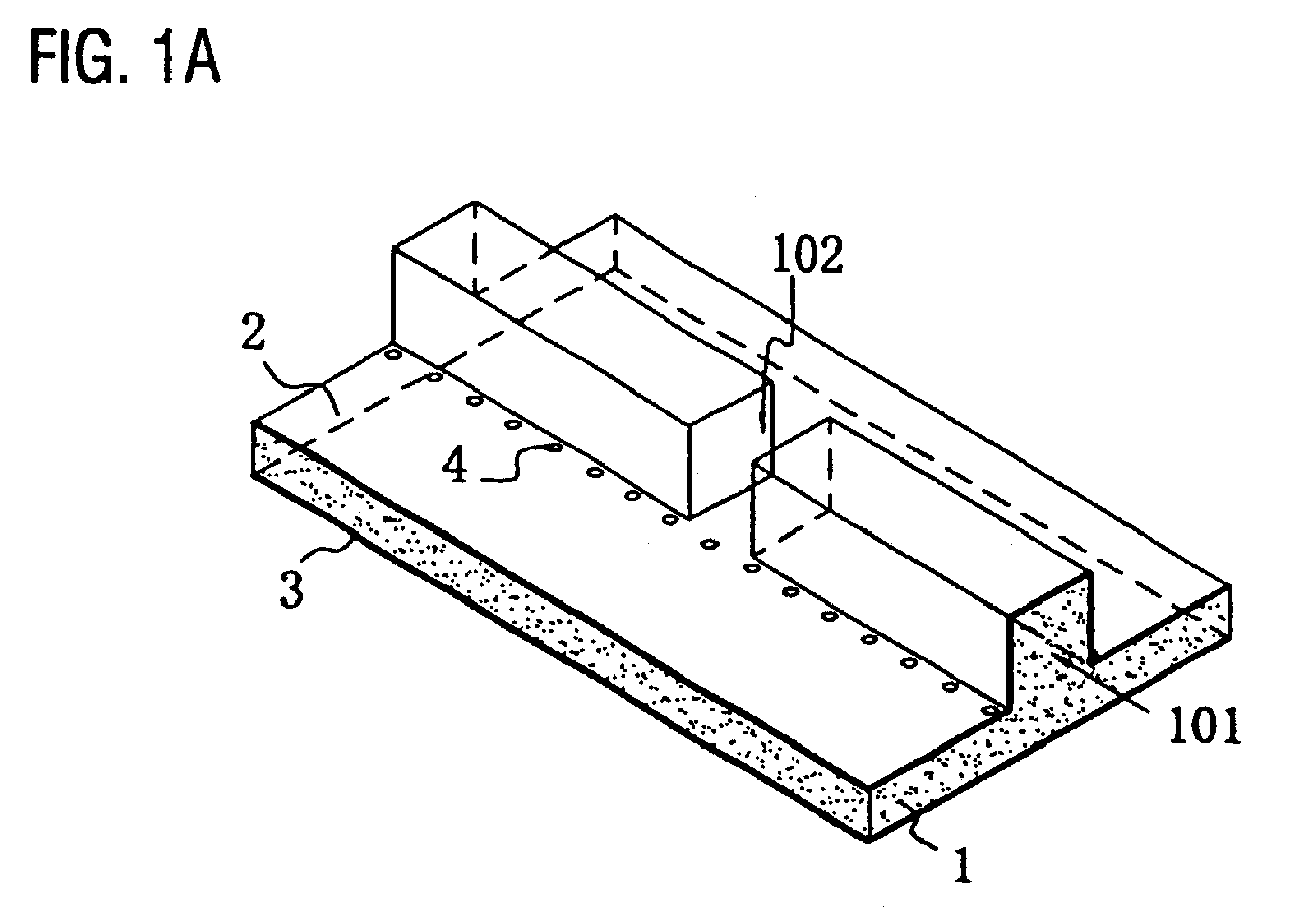
- Figs. 1A and 1B are perspective views of the transmission line wherein Fig. 1A shows a lower side and Fig. 1B shows an upper side.
- a dielectric substrate 1 In Figs. 1A and 1B, a dielectric substrate 1, a lower-surface electrode 2, an upper-surface electrode 3, through-holes 4, coplanar lines 5, a circuit element 6, protrusions 101, and a discontinuous portion 102 are shown.
- the protrusions 101 extend in line one after another in a direction perpendicular to the cross section in a part of the dielectric substrate 1, with the discontinuous portion 102 therebetween.
- the lower-surface electrode 2 is formed on a main surface of the dielectric substrate 1 provided with the protrusions 101 and on the outer surfaces (side surfaces and upper surface) of the protrusions 101.
- the upper-surface electrode 3 is formed on substantially the whole area of the surface that is opposite to the lower-surface electrode 2. Further, the plurality of through-holes 4 for connecting the lower-surface electrode 2 and the upper-surface electrode 3, which are formed on both surfaces of the dielectric substrate 1, are aligned on both sides of the protrusions 101 along the direction in which the protrusions 101 extend.
- the width of each of the protrusions 101 is 1/2 or less of the wavelength at an operating frequency in the dielectric substrate 1, and the height, that is, the distance from the upper surface of the dielectric substrate 1 to the lower surface of the protrusions 101 is 1/2 or more of the wavelength at an operating frequency in the dielectric substrate 1.
- the aligned plurality of through-holes 4 equivalently define a wall of a transmission path. Accordingly, electromagnetic waves propagate in a mode similar to the TE 10 mode, where two mutually opposing side surfaces of the protrusions 101 are defined as H surfaces and the lower surfaces of the protrusions 101 and the upper surface of the dielectric substrate 1 are defined as E surfaces.
- the effective thickness of the transmission path is the thickness of the dielectric substrate 1 at the discontinuous portion 102, where no protrusion exists.
- the cut-off frequency of the transmission path increases and thus the electromagnetic waves at the operating frequency are cut off and do not propagate.
- the coplanar lines 5 are formed on the upper-surface electrode 3 such that the edges of the coplanar lines 5 are located at positions facing the edges of the protrusions 101, which are separated by the discontinuous portion 102. Also, the circuit element 6 connected to the coplanar lines 5 is mounted on the dielectric substrate 1.
- Fig. 2 is a sectional view of the dielectric substrate 1 taken along the direction in which the protrusions 101 extend.
- Fig. 2 the dielectric substrate 1, the lower-surface electrode 2, the upper-surface electrode 3, the coplanar lines 5, the protrusions 101, and the discontinuous portion 102 are shown.
- the broken lines indicate the magnetic field distribution of the TE 10 mode.
- electromagnetic fields are induced in the coplanar lines 5 formed on the surface of the dielectric substrate 1 by the TE 10 mode which propagates through the transmission path formed by the protrusions 101.
- the transmission path formed by the protrusions 101 of the dielectric substrate 1 is coupled by the electromagnetic fields to the coplanar lines 5 formed on the upper-surface electrode 3.
- the transmission of a signal, which has been transmitted through the transmission path formed by one of the protrusions 101, is interrupted at the discontinuous portion 102, but the signal is transmitted to one of the coplanar lines 5.
- the signal transmitted by the coplanar line 5 is input to the circuit element 6 and the circuit element 6 outputs an output signal.
- the output signal is transmitted from the circuit element 6 through the other coplanar line 5 to the transmission path formed by the other protrusion 101, which is coupled to the coplanar line 5 by the electromagnetic fields, and is output to the external circuit.
- circuit element 6 when the circuit element 6 is an FET, an amplifier having a simple configuration can be achieved and mounted on the transmission path, by making the transmission path function as input/output terminals.
- a large attenuation can be obtained by a line penetration (isolation) characteristic between the input-side of the transmission path and the output-side of the transmission path.
- Fig. 3A is a table showing a plurality of parameters of the transmission line
- Fig. 3B is a perspective view indicating each parameter.
- Fig. 4 is a diagram showing the isolation characteristic of the circuit when the length of the discontinuous portion (gap) in the transmission line constituted by the parameters shown in Fig. 3A is changed.
- the frequency is 76.5 GHz.
- the isolation characteristic is improved as the length of the discontinuous portion (gap) increases.
- Fig. 5 is a perspective view of the transmission line.
- Fig. 5 the dielectric substrate 1, the lower-surface electrode 2, the upper-surface electrode 3, the through-holes 4, the protrusions 101, and a protrusion 103 are shown.
- the protrusion 103 In the transmission line shown in Fig. 5, the protrusion 103, whose height is lower than that of the protrusions 101, is provided between the protrusions 101.
- the configuration of the transmission line is otherwise the same as the one shown in Figs. 1A and 1B.
- the protrusion 103 is formed such that the distance from the upper-surface electrode 3 of the dielectric substrate 1 to the lower surface of the protrusion 103 is shorter than 1/2 of the wavelength of a transmission signal. Accordingly, the height of the H surface decreases, the cut-off frequency of the transmission path increases, the TE 10 mode is interrupted at the protrusion 103, and thus electromagnetic waves are not transmitted via the protrusion 103 between the protrusions 101.
- leakage between the transmission paths formed by the protrusions 101 can be suppressed and the penetration characteristic of the circuit including the circuit element mounted on the dielectric substrate and the transmission line can be improved.
- Fig. 6 is a perspective view of the transmission line.
- Fig. 6 the dielectric substrate 1, the lower-surface electrode 2, the upper-surface electrode 3, the through-holes 4, the protrusions 101, and indented portions 104 are shown.
- the indented portions 104 are provided between the protrusions 101 which extend one after another, such that the indented portions 104 are recessed at the two sides in the width direction of the protrusions 101.
- the configuration of the transmission line is otherwise the same as the one shown in Figs. 1A and 1B.
- the operation is the same as that of the transmission line shown in Fig. 5, utilizing the TE 01 mode in which the electromagnetic fields are turned by 90 degrees.
- the indented portions 104 contribute to suppress leakage between the protrusions 101, and thus the transmission characteristic of the circuit including the circuit element mounted on the dielectric substrate 1 and the transmission line can be improved.
- Figs. 7A and 7B are perspective views of the transmission line.
- Figs. 7A and 7B the dielectric substrate 1, the lower-surface electrode 2, the upper-surface electrode 3, the through-holes 4, the protrusions 101, and the discontinuous portion 102 are shown.
- the through-holes 4 provided in the discontinuous portion 102 equivalently function as a conductor wall, and thus the interruption effect of electromagnetic waves can be further improved.
- Fig. 8 is a perspective view of the transmission line.
- the dielectric substrate 1, the lower-surface electrode 2, the upper-surface electrode 3, the through-holes 4, protrusions 101a and 101b, and the discontinuous portion 102 are shown.
- the protrusions 101a and 101b which are separated by the discontinuous portion 102, have different heights.
- the configuration of the transmission line is otherwise the same as the one shown in Figs. 1A and 1B.
- different cut-off frequencies can be obtained in the transmission path formed by the protrusion 101a and the transmission path formed by the protrusion 101b.
- the frequency of an input signal is different from that of an output signal in a multiplier or the like
- by decreasing the height of the protrusion on the output-side so that the cut-off frequency on the output-side is higher than the frequency of an input signal leakage of waves directly between the input-side of the transmission path and the output-side of the transmission path can be prevented and transmission of an input signal frequency can be interrupted.
- Fig. 9 is a perspective view of the transmission line.
- Fig. 9 the dielectric substrate 1, the lower-surface electrode 2, the upper-surface electrode 3, the through-holes 4, the protrusions 101a and 101b, and a protrusion 105 are shown.
- the protrusion 105 is provided between the protrusions 101a and 101b, which have different heights.
- the protrusion 105 is shorter in height and width than the protrusions 101a and 101b.
- the configuration of the transmission line is otherwise the same as the one shown in Fig. 8.
- Fig. 10 shows a circuit arrangement that can be applied to any of the other embodiments of the invention.
- Fig. 10 is a perspective view of a transmission line and shows the dielectric substrate 1, the lower-surface electrode 2, the upper-surface electrode 3, the through-holes 4, and a circuit arrangement comprising slits 7, and a circuit element 8.
- a pattern for example, a coplanar line, a slot line, and a microstrip line
- the pattern can be mounted in a predetermined position on a surface of the dielectric substrate so as to be coupled to the transmission path formed by the protrusions.
- a radar device Next, the configuration of a radar device will be described with reference to Figs. 11 and 12, as an example of an integrated circuit and a transmitter-receiver using the same.
- Fig. 11 is a perspective view of a dielectric substrate viewed from the side of the electronic component mounting face and Fig. 12 is an equivalent circuit thereof.
- the dielectric substrate 1 has protrusions (not shown) which extend in line one after another on the lower surface thereof, electrodes on both surfaces thereof, and a plurality of through-holes aligned along the protrusions at both sides of the protrusions, thereby forming a transmission line.
- the transmission line can be seen from the alignment pattern of the through-holes. That is, six transmission lines, which are roughly indicated by G1, G2, G3, G4, G5, and G7, are formed. G6 is a portion for connecting G1 and G2, but no protrusion is formed on its lower surface.
- a voltage-controlled oscillator (VCO) connected to a coplanar line is provided on the upper surface of the dielectric substrate 1.
- the coplanar line is coupled to the transmission line indicated by G1.
- an amplifier circuit including an FET connected by coplanar lines is provided between the transmission lines G1 and G2.
- the lower surface opposite to the position of G6 between G1 and G2 has no protrusion, and thus a signal can be transmitted from G1 to G2 through the coplanar lines without leakage. Then, the signal amplified by the FET is transmitted from the coplanar line to G2.
- a slot antenna is provided at the end of the transmission line G3 and the slot antenna radiates a transmission signal in the direction perpendicular to the dielectric substrate 1.
- the portion where the transmission lines G2 and G5 are close to each other constitutes a directional coupler.
- the signal, which is power-distributed by the directional coupler, is coupled as a local signal to a coplanar line to which one diode of a mixer circuit is connected.
- the other line G7 is coupled to a coplanar line and connected to a resistor, thereby functioning as a terminator of the directional coupler.
- a circulator (not shown) is provided at the branching point of a Y-shape constituted by the transmission lines G2, G3, and G4.
- the circulator is constituted by providing a resonator made of a circular ferrite plate and locating a permanent magnet for applying a static magnetic field in the direction perpendicular to the ferrite plate.
- the illustration of the circulator is omitted in Fig. 11.
- a reception signal from the slot antenna can be transmitted through the circulator and the transmission line G4, and is coupled to a coplanar line to which the other diode of the mixer circuit is connected.
- the two diodes in the mixer circuit function as a balanced mixer circuit and an IF signal is output to the external circuit.
- Fig. 12 is a block diagram of the radar device.
- an oscillation signal from the VCO is amplified by the amplifier AMP and transmitted to the antenna ANT as a transmission signal via the directional coupler CPL and the circulator CIR.
- the reception signal from the circulator CIR and the local signal from the directional coupler CPL are transmitted to the mixer MIX and the mixer outputs an intermediate frequency signal IF.
- any communication device in which a transmission signal is transmitted to another communication device and a transmission signal is received from the other communication device can be configured in the same way.
Landscapes
- Waveguides (AREA)
- Microwave Amplifiers (AREA)
- Structure Of Printed Boards (AREA)
Abstract
Description
Claims (19)
- A dielectric-waveguide-type transmission line comprising:a dielectric substrate 1 having two opposed main surfaces;a plurality of protrusions (101; 101a, 101b) aligned, one after another, on at least one main surface of the dielectric substrate (1);electrodes (2, 3) formed on both main surfaces of the dielectric substrate 1 and on outer surfaces of the protrusions (101; 101a, 101b);a plurality of through-holes 4 connecting the electrodes (2, 3), the plurality of through holes (4) being aligned along both sides of the protrusions (101; 101a, 101b), the protrusions (101; 101a, 101b), functioning as a main transmission line;an interrupting structure (102; 103; 104; 105) which divides the main transmission line into transmission line segments to interrupt a transmission signal; anda circuit (6; 8) which couples said transmission line segments separated by the interrupting structure (102; 103; 104; 105), the circuit (6; 8) being provided on the other main surface of the dielectric substrate (1).
- The transmission line according to Claim (1 or 2), wherein the interrupting structure comprises a protrusion (103; 105) having a predetermined length and a height which is less than a height of the protrusions (101; 101a, 101b).
- The transmission line according to any of Claims (1 to 3), further comprising additional through-holes (4) connecting the electrodes (2, 3), the additional through-holes (4) being provided in an area (102) between two adjacent transmission line segments.
- The transmission line according to any of Claims (1 to 4), wherein a protrusion (101a, 101b) corresponding to one transmission line segment has a different height from another protrusion (101a, 101b) corresponding to an adjacent transmission line segment.
- The transmission line according to any of Claims (1 to 5), wherein the interrupting structure comprises a gap between two adjacent transmission line segments.
- An integrated circuit comprising the transmission line according to any Claims (1 to 6), electronic components mounted on the other main surface of the dielectric substrate (1), said circuit being connected to said electronic components.
- A transceiver comprising the integrated circuit according to Claim (7), said integrated circuit being connected to at least one of a transmission circuit and a reception circuit.
- A transceiver comprising the transmission line according to any of Claims (1 to 6), said transmission line being connected to at least one of a transmission circuit and a reception circuit.
- A dielectric-waveguide-type transmission line comprising:a dielectric substrate 1 having two opposed main surfaces;a plurality of aligned protrusions (101; 101a, 101b) on one main surface of the dielectric substrate (1), the protrusions (101; 101a, 101b) functioning as a main transmission line;electrodes (2,3), formed on both main surfaces of the dielectric substrate (1) and on outer surfaces of the protrusions (101; 101a, 101b);a plurality of through-holes 4 connecting the electrodes (2,3), the plurality of through holes (4) being aligned along both sides of the protrusions (101; 101a, 101b)an interrupting structure (102; 103; 104; 105) disposed between two adjacent protrusions which divides the main transmission line into transmission line segments to interrupt a transmission signal carried thereon; anda circuit (6; 8) which couples said transmission line segments divided by the interrupting structure (102; 103; 104; 105), the circuit (6; 8) carrying said transmission signal between said segments.
- The transmission line according to Claim (10), wherein said circuit (6; 8) is disposed on the other main surface of the dielectric substrate (1).
- The transmission line according to Claim (10 or 11), wherein the interrupting structure comprises an additional protrusion (103; 105) having a predetermined length and a height which is less than a height of the two adjacent protrusions (101; 101a, 101b).
- The transmission line according to any of Claims (10-12), wherein the interrupting structure comprises an additional protrusion (104; 105) having a predetermined length and a width which is narrower than a width of the two adjacent protrusions (101; 101a, 101b).
- The transmission line according to any of Claims (10-13), further comprising additional through-holes (4) connecting the electrodes, the additional through-holes (4) being provided in an area (102) between said two adjacent protrusions (101a, 101b).
- The transmission line according to any of Claims (10-14), wherein a protrusion (101a, 101b) corresponding to one transmission line segment has a different height from another protrusion (101a, 101b) corresponding to an adjacent transmission line segment.
- The transmission line according to any of Claims (10-15), wherein the interrupting structure comprises a gap between two adjacent transmission line segments.
- The transmission line according to Claim (16), further comprising additional through-holes connecting the electrodes, the additional through-holes being provided in said gap.
- An integrated circuit comprising the transmission line according to any of Claims (10-17), electronic components mounted on the other main surface of the dielectric substrate, said circuit being connected to said electronic components.
- A transceiver comprising the integrated circuit according to Claim (18), said integrated circuit being connected to at least one of a transmission circuit and a reception circuit.
- A transceiver comprising the transmission line according to any of Claims (10-17), said transmission line being connected to at least one of a transmission circuit and a reception circuit.
Applications Claiming Priority (2)
| Application Number | Priority Date | Filing Date | Title |
|---|---|---|---|
| JP2001158609A JP3531624B2 (en) | 2001-05-28 | 2001-05-28 | Transmission line, integrated circuit and transmitting / receiving device |
| JP2001158609 | 2001-05-28 |
Publications (3)
| Publication Number | Publication Date |
|---|---|
| EP1263078A2 true EP1263078A2 (en) | 2002-12-04 |
| EP1263078A3 EP1263078A3 (en) | 2003-09-10 |
| EP1263078B1 EP1263078B1 (en) | 2006-03-01 |
Family
ID=19002298
Family Applications (1)
| Application Number | Title | Priority Date | Filing Date |
|---|---|---|---|
| EP02011840A Expired - Lifetime EP1263078B1 (en) | 2001-05-28 | 2002-05-28 | Transmission line, integrated circuit and transmitter-receiver |
Country Status (4)
| Country | Link |
|---|---|
| US (1) | US6614332B2 (en) |
| EP (1) | EP1263078B1 (en) |
| JP (1) | JP3531624B2 (en) |
| DE (1) | DE60209401T2 (en) |
Cited By (2)
| Publication number | Priority date | Publication date | Assignee | Title |
|---|---|---|---|---|
| CN107240746A (en) * | 2016-03-29 | 2017-10-10 | 日本电产艾莱希斯株式会社 | Microwave IC waveguide assembly modules |
| CN108432037A (en) * | 2015-09-24 | 2018-08-21 | 加普韦夫斯公司 | Waveguides and transmission lines in gaps between parallel conducting surfaces |
Families Citing this family (16)
| Publication number | Priority date | Publication date | Assignee | Title |
|---|---|---|---|---|
| DE60208244T2 (en) * | 2001-01-12 | 2006-06-29 | Murata Manufacturing Co., Ltd., Nagaokakyo | Transmission line arrangement, integrated circuit and transmitter-receiver device |
| JP3678194B2 (en) * | 2001-12-04 | 2005-08-03 | 株式会社村田製作所 | Transmission line and transmission / reception device |
| JP3695395B2 (en) * | 2002-01-09 | 2005-09-14 | 株式会社村田製作所 | Transmission line and transmission / reception device |
| WO2006027828A1 (en) * | 2004-09-07 | 2006-03-16 | Mitsubishi Denki Kabushiki Kaisha | Electric power distributing apparatus, electric power combining apparatus, mono-pulse signal combining circuit, array antenna power supplying circuit, and beam shaping circuit |
| US7109823B1 (en) | 2005-01-07 | 2006-09-19 | Hrl Lab Llc | Image guide coupler switch |
| JP4345850B2 (en) | 2006-09-11 | 2009-10-14 | ソニー株式会社 | Communication system and communication apparatus |
| KR100780419B1 (en) * | 2006-09-27 | 2007-11-29 | 주식회사 케이엠더블유 | High frequency switch |
| US20080242331A1 (en) * | 2007-03-26 | 2008-10-02 | Broadcom Corporation | High frequency testing infrastructure |
| US8564478B2 (en) * | 2008-03-31 | 2013-10-22 | Kyocera Corporation | High-frequency module and method of manufacturing the same, and transmitter, receiver, transceiver, and radar apparatus comprising the high-frequency module |
| EP2277232B1 (en) * | 2008-04-16 | 2016-06-08 | Telefonaktiebolaget LM Ericsson (publ) | A waveguide transition arrangement |
| JP5123154B2 (en) * | 2008-12-12 | 2013-01-16 | 東光株式会社 | Dielectric waveguide-microstrip conversion structure |
| US9561730B2 (en) | 2010-04-08 | 2017-02-07 | Qualcomm Incorporated | Wireless power transmission in electric vehicles |
| US10343535B2 (en) | 2010-04-08 | 2019-07-09 | Witricity Corporation | Wireless power antenna alignment adjustment system for vehicles |
| WO2014171292A1 (en) * | 2013-04-18 | 2014-10-23 | ソニー株式会社 | Connector device and wireless transmission system |
| CN104882656B (en) * | 2015-04-27 | 2017-12-29 | 南通大学 | A kind of balanced type transition circuit of micro-strip to substrate integration wave-guide |
| CN111668584B (en) * | 2020-06-15 | 2022-01-28 | 北京无线电测量研究所 | Waveguide magic T structure and waveguide magic T comprising same |
Family Cites Families (13)
| Publication number | Priority date | Publication date | Assignee | Title |
|---|---|---|---|---|
| US5262739A (en) * | 1989-05-16 | 1993-11-16 | Cornell Research Foundation, Inc. | Waveguide adaptors |
| JPH0653711A (en) | 1992-07-28 | 1994-02-25 | Fukushima Nippon Denki Kk | Waveguide line |
| JP3166897B2 (en) * | 1995-08-18 | 2001-05-14 | 株式会社村田製作所 | Non-radiative dielectric line and its integrated circuit |
| JP2998614B2 (en) * | 1995-10-04 | 2000-01-11 | 株式会社村田製作所 | Dielectric line |
| JP3686736B2 (en) | 1996-08-30 | 2005-08-24 | 京セラ株式会社 | Dielectric waveguide line and wiring board |
| JP3493265B2 (en) * | 1996-09-30 | 2004-02-03 | 京セラ株式会社 | Dielectric waveguide line and wiring board |
| JP3120757B2 (en) * | 1997-06-17 | 2000-12-25 | 株式会社村田製作所 | Dielectric line device |
| JP3269448B2 (en) * | 1997-07-11 | 2002-03-25 | 株式会社村田製作所 | Dielectric line |
| US6515562B1 (en) * | 1998-04-23 | 2003-02-04 | Kyocera Corporation | Connection structure for overlapping dielectric waveguide lines |
| JPH11308003A (en) * | 1998-04-24 | 1999-11-05 | Tokimec Inc | Nonradioactive dielectric line, mode transformation circuit, and high frequency circuit |
| JP3517148B2 (en) | 1999-03-01 | 2004-04-05 | 京セラ株式会社 | Connection structure between dielectric waveguide line and high-frequency line conductor |
| JP3414383B2 (en) | 2001-01-12 | 2003-06-09 | 株式会社村田製作所 | Transmission line, integrated circuit and transmitting / receiving device |
| DE60208244T2 (en) * | 2001-01-12 | 2006-06-29 | Murata Manufacturing Co., Ltd., Nagaokakyo | Transmission line arrangement, integrated circuit and transmitter-receiver device |
-
2001
- 2001-05-28 JP JP2001158609A patent/JP3531624B2/en not_active Expired - Fee Related
-
2002
- 2002-04-19 US US10/127,235 patent/US6614332B2/en not_active Expired - Fee Related
- 2002-05-28 DE DE60209401T patent/DE60209401T2/en not_active Expired - Lifetime
- 2002-05-28 EP EP02011840A patent/EP1263078B1/en not_active Expired - Lifetime
Cited By (3)
| Publication number | Priority date | Publication date | Assignee | Title |
|---|---|---|---|---|
| CN108432037A (en) * | 2015-09-24 | 2018-08-21 | 加普韦夫斯公司 | Waveguides and transmission lines in gaps between parallel conducting surfaces |
| CN107240746A (en) * | 2016-03-29 | 2017-10-10 | 日本电产艾莱希斯株式会社 | Microwave IC waveguide assembly modules |
| US10651138B2 (en) | 2016-03-29 | 2020-05-12 | Nidec Corporation | Microwave IC waveguide device module |
Also Published As
| Publication number | Publication date |
|---|---|
| EP1263078A3 (en) | 2003-09-10 |
| JP2002353708A (en) | 2002-12-06 |
| US6614332B2 (en) | 2003-09-02 |
| JP3531624B2 (en) | 2004-05-31 |
| DE60209401T2 (en) | 2006-08-03 |
| US20020175784A1 (en) | 2002-11-28 |
| EP1263078B1 (en) | 2006-03-01 |
| DE60209401D1 (en) | 2006-04-27 |
Similar Documents
| Publication | Publication Date | Title |
|---|---|---|
| EP1263078B1 (en) | Transmission line, integrated circuit and transmitter-receiver | |
| EP1227536A1 (en) | Transmission line assembly, integrated circuit, and transmitter-receiver apparatus | |
| EP0820114A1 (en) | Multilayer dielectric line circuit | |
| US6538526B2 (en) | Transmission line connection structure, high frequency module, and communication device | |
| US6888429B2 (en) | Transmission line with a projecting dielectric part having an opposing coplanar line and transceiver | |
| US6931246B2 (en) | Line coupling structure, mixer, and receiving/transmitting apparatus comprised of suspended line and dielectric waveguide | |
| KR100319811B1 (en) | Nonreciprocal Circuit Device and Nonreciprocal Circuit Apparatus, and Transceiver using the Same | |
| JP3565184B2 (en) | Dielectric waveguide, integrated circuit, and transceiver | |
| US6606000B2 (en) | Radio-frequency amplifier, radio-frequency module and communication device | |
| KR100432793B1 (en) | Mixer, radar module, and communication apparatus incorporating the same | |
| US6232854B1 (en) | Dielectric resonator device, dielectric filter, oscillator, sharing device, and electronic apparatus | |
| US6359526B1 (en) | Nonreciprocal circuit device including dielectric wave guide and a lower dielectric constant medium | |
| US6496080B1 (en) | Dielectric waveguide nonreciprocal circuit device with a non-interfering magnetic member support | |
| JP4224909B2 (en) | Line conversion structure, high-frequency circuit, and wireless device | |
| EP0957528A1 (en) | Nonreciprocal circuit device including dielectric wave guide, dielectric wave guide device and radio device | |
| JP2002217613A (en) | Transmission line, integrated circuit and transmitting/ receiving device | |
| JP2007053440A (en) | Suspended stripline device and transmitting/receiving apparatus | |
| KR20050016116A (en) | Directional coupler and high-frequency circuit device | |
| JP2006115333A (en) | Resonance device, oscillator, filter and radio equipment | |
| JP2002176302A (en) | Directional coupler, high frequency module and communication equipment | |
| JP2002237705A (en) | Non-radioactive dielectric line and high frequency circuit component and high frequency circuit module | |
| JP2008054073A (en) | Transmission mode conversion structure |
Legal Events
| Date | Code | Title | Description |
|---|---|---|---|
| PUAI | Public reference made under article 153(3) epc to a published international application that has entered the european phase |
Free format text: ORIGINAL CODE: 0009012 |
|
| 17P | Request for examination filed |
Effective date: 20020528 |
|
| AK | Designated contracting states |
Kind code of ref document: A2 Designated state(s): AT BE CH CY DE DK ES FI FR GB GR IE IT LI LU MC NL PT SE TR |
|
| AX | Request for extension of the european patent |
Free format text: AL;LT;LV;MK;RO;SI |
|
| PUAL | Search report despatched |
Free format text: ORIGINAL CODE: 0009013 |
|
| AK | Designated contracting states |
Kind code of ref document: A3 Designated state(s): AT BE CH CY DE DK ES FI FR GB GR IE IT LI LU MC NL PT SE TR |
|
| AX | Request for extension of the european patent |
Extension state: AL LT LV MK RO SI |
|
| AKX | Designation fees paid |
Designated state(s): DE FR GB |
|
| GRAP | Despatch of communication of intention to grant a patent |
Free format text: ORIGINAL CODE: EPIDOSNIGR1 |
|
| GRAS | Grant fee paid |
Free format text: ORIGINAL CODE: EPIDOSNIGR3 |
|
| GRAA | (expected) grant |
Free format text: ORIGINAL CODE: 0009210 |
|
| AK | Designated contracting states |
Kind code of ref document: B1 Designated state(s): DE FR GB |
|
| REG | Reference to a national code |
Ref country code: GB Ref legal event code: FG4D |
|
| REF | Corresponds to: |
Ref document number: 60209401 Country of ref document: DE Date of ref document: 20060427 Kind code of ref document: P |
|
| ET | Fr: translation filed | ||
| PLBE | No opposition filed within time limit |
Free format text: ORIGINAL CODE: 0009261 |
|
| STAA | Information on the status of an ep patent application or granted ep patent |
Free format text: STATUS: NO OPPOSITION FILED WITHIN TIME LIMIT |
|
| 26N | No opposition filed |
Effective date: 20061204 |
|
| PGFP | Annual fee paid to national office [announced via postgrant information from national office to epo] |
Ref country code: GB Payment date: 20130522 Year of fee payment: 12 Ref country code: DE Payment date: 20130522 Year of fee payment: 12 |
|
| PGFP | Annual fee paid to national office [announced via postgrant information from national office to epo] |
Ref country code: FR Payment date: 20130531 Year of fee payment: 12 |
|
| REG | Reference to a national code |
Ref country code: DE Ref legal event code: R119 Ref document number: 60209401 Country of ref document: DE |
|
| GBPC | Gb: european patent ceased through non-payment of renewal fee |
Effective date: 20140528 |
|
| REG | Reference to a national code |
Ref country code: DE Ref legal event code: R119 Ref document number: 60209401 Country of ref document: DE Effective date: 20141202 |
|
| REG | Reference to a national code |
Ref country code: FR Ref legal event code: ST Effective date: 20150130 |
|
| PG25 | Lapsed in a contracting state [announced via postgrant information from national office to epo] |
Ref country code: DE Free format text: LAPSE BECAUSE OF NON-PAYMENT OF DUE FEES Effective date: 20141202 |
|
| PG25 | Lapsed in a contracting state [announced via postgrant information from national office to epo] |
Ref country code: GB Free format text: LAPSE BECAUSE OF NON-PAYMENT OF DUE FEES Effective date: 20140528 Ref country code: FR Free format text: LAPSE BECAUSE OF NON-PAYMENT OF DUE FEES Effective date: 20140602 |