FIELD OF THE INVENTION
The present invention is related in general to the field
of electronic systems and semiconductor devices, and more
specifically to structure and fabrication methods of MOS
transistors, which have an additional implant under the channel
compared to standard technology.
DESCRIPTION OF THE RELATED ART
Integrated circuits (ICs) may be severely damaged by
electrostatic discharge (ESD) events. A major source of ESD
exposure to ICs is from the charged human body ("Human Body
Model", HBM); the discharge of the human body generates peak
currents of several amperes to the IC for about 100 ns. A
second source of ESD is from metallic objects ("machine model",
MM); it can generate transients with significantly higher rise
times than the HBM ESD source. A third source is described by
the "charged device model" (CDM), in which the IC itself becomes
charged and discharges to ground in the opposite direction than
the HBM and MM ESD sources. More detail on ESD phenomena and
approaches for protection in ICs can be found in A. Amerasekera
and C. Duvvury, "ESD in Silicon Integrated Circuits" (John Wiley
& Sons LTD. London 1995), and C. Duvvury, "ESD: Design for IC
Chip Quality and Reliability" (Int. Symp. Quality in El.
Designs, 2000, pp. 251-259; references of recent literature).
ESD phenomena in ICs are growing in importance as the
demand for higher operating speed, smaller operating voltages,
higher packing density and reduced cost drives a reduction of
all device dimensions. This generally implies thinner
dielectric layers, higher doping levels with more abrupt doping
transitions, and higher electric fields - all factors that
contribute to an increased sensitivity to damaging ESD events.
The most common protection schemes used in metal-oxide-semiconductor
(MOS) ICs rely on the parasitic bipolar transistor
associated with an NMOS device whose drain is connected to the
pin to be protected and whose source is tied to ground. The
protection level or failure threshold can be set by varying the
NMOS device width from the drain to the source under the gate
oxide of the NMOS device. Under stress conditions, the dominant
current conduction path between the protected pin and ground
involves the parasitic bipolar transistor of that NMOS device.
This parasitic bipolar transistor operates in the snapback
region under pin positive with respect to ground stress events.
The dominant failure mechanism, found in the NMOS
protection device operating as a parasitic bipolar transistor in
snapback conditions, is the onset of second breakdown. Second
breakdown is a phenomenon that induces thermal runaway in the
device wherever the reduction of the impact ionization current
is offset by the thermal generation of carriers. Second
breakdown is initiated in a device under stress as a result of
self-heating. The peak NMOS device temperature, at which second
breakdown is initiated, is known to increase with the stress
current level.
Many circuits have been proposed and implemented for
protecting ICs from ESD. One method that is used to improve ESD
protection for ICs is biasing the substrate of ESD protection
circuits on an IC. Such substrate biasing can be effective at
improving the response of a multi-finger MOS transistor that is
used to conduct an ESD discharge to ground. However, substrate
biasing can cause the threshold voltages for devices to change
from their nominal values, which may affect device operation.
In addition, substrate biasing under steady-state conditions
causes heat generation and increases power losses.
Solutions offered in known technology require additional
IC elements, silicon real estate, and/or process steps
(especially photomask alignment steps). Their fabrication is,
therefore, expensive. Examples of device structures and methods
are described in US. Patents # 5,539,233, issued 07/23/1996
(Amerasekera et al., "Controlled Low Collector Breakdown Voltage
Vertical Transistor for ESD Protection Circuits"); # 5,793,083,
issued 08/11/1998 (Amerasekera et al., "Method for Designing
Shallow Junction, Salicided NMOS Transistors with Decreased
Electrostatic Discharge Sensitivity"); # 5,940,258, issued
08/17/1999 (Duvvury, "Semiconductor ESD Protection Circuit"); #
6,137,144, issued 10/24/2000, and # 6,143,594, issued 11/07/2000
(Tsao et al, "On-Chip ESD Protection in Dual Voltage CMOS); and
U.S. Patent Application # 09/456,036, filed 12/03/1999
(Amerasekera et al., "Electrostatic Discharge Device and
Method").
The influence of substrate well profiles on the device
ESD performance is investigated, for instance, in "Influence of
Well Profile and Gate Length on the ESD Performance of a Fully
Silicided 0.25 µm CMOS Technology" (K. Bock, C. Russ, G.
Badenes, G. Groeseneken and L. Deferm, Proc. EOS/ESD Symp.,
1997, pp. 308-315). However, known technology recommends only a
lower epitaxial doping or a lower implant dose as methods to
increase the p-well resistance.
The challenge of cost reduction implies a drive for
minimizing the number of process steps, especially a minimum
number of photomask steps, and the application of standardized
process conditions wherever possible. These constraints should
be kept in mind when additional process steps or new process
conditions are proposed to improve ESD insensitivity without
sacrificing any desirable device characteristics. An urgent
need has, therefore, arisen for a coherent, low-cost method of
enhancing ESD insensitivity without the need for additional,
real-estate consuming protection devices. The device structure
should further provide excellent electrical performance,
mechanical stability and high reliability. The fabrication
method should be simple, yet flexible enough for different
semiconductor product families and a wide spectrum of design and
process variations. Preferably, these innovations should be
accomplished without extending production cycle time, and using
the installed equipment, so that no investment in new
manufacturing machines is needed.
SUMMARY OF THE INVENTION
A lateral NMOS transistor in a p-well, bordered laterally
on each side by an isolation region and vertically by a stopping
region, has a n-source and a n- drain, each comprising a shallow
region extending to the transistor gate and a deeper region
recessed from the gate. The transistor further has in its p-well
a region of higher resistivity than the remainder of the
well; this region extends laterally from one recessed region to
the other, and vertically from a depth just below the depletion
regions to the depth of the stopping region.
According to the invention, this region of higher p-type
resistivity is created by an ion implant of compensating n-doping,
such as arsenic or phosphorus, using the same photomask
already used for implants adjusting the threshold voltage and
creating the p-well and channel stop.
In an ESD event, this region of higher resistivity
increases the current gain of the parasitic lateral npn bipolar
transistor and thus raises the current It2, which initiates the
thermal breakdown with its destructive localized heating.
When the gate, source and substrate terminals are at 0 V
and the drain at positive potential, the current gain β of the
lateral bipolar npn transistor in the ESD event is defined as
β = (Id - Igen)/(Igen - Isub),
where
It is an aspect of the invention that the region of
higher resistivity is the substrate of the transistor, enabling
full functioning of the transistor while not affecting operation
of neighboring active devices.
Another aspect of the invention is that the region of
higher resistivity improves the ESD protection of the transistor
without decreasing latch-up robustness or increasing inadvertent
substrate current-induced body biasing of neighboring
transistors.
Another aspect of the invention is that it is equally
applicable to PMOS transistors; the conductivity types of the
semiconductor and the ion implant types are simply reversed.
The method of fabricating the region of higher
resistivity under the active area of a high-voltage NMOS
transistor having a gate comprises the steps of depositing a
photoresist layer over the transistor and opening a window in
this layer over the active area of the transistor; then
implanting, at high energy, n-doping ions into the p-type
semiconductor substrate through the window, creating a deep
region having a net p-type doping lower than that of the p-type
semiconductor remote from the transistor active area. A
preferred depth of the region is between 50 and 150 nm. A
region too deep would require higher implant energy with
possibly more damage and thus higher junction leakage current or
junction isolation failure.
It is an essential aspect of the present invention that
this high-energy ion implant is performed without the need for a
new photomask step. This economical feature renders the
additional high-energy ion implant step of the present invention
exceedingly inexpensive.
The technical advances represented by the invention, as
well as the aspects thereof, will become apparent from the
following description of the preferred embodiments of the
invention, when considered in conjunction with the accompanying
drawings and the novel features set forth in the appended
claims.
BRIEF DESCRIPTION OF THE DRAWINGS
FIG. 1 is a simplified and schematic cross section
through a lateral MOS transistor, illustrating the current flow
at an electrostatic discharge event.
FIG. 2 is a schematic plot of drain (collector) current,
on a logarithmic scale, as a function of drain voltage, on a
linear scale, illustrating the onset of the second breakdown
phenomenon.
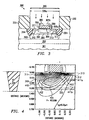
FIG. 3 schematically presents a cross section of a
lateral MOS transistor with a photoresist window opened for the
high energy ion implant according to the invention.
FIG. 4 illustrates schematically, yet in more detail, the
cross section of the region of the compensating ion implant of
the invention.
FIG. 5 illustrates an example of the doping profiles
employed by the invention.
FIG. 6 depicts a schematic cross section of the MOS
transistor showing another embodiment of the invention.
FIGs. 7 to 12 are schematic and simplified cross sections
of an MOS transistor illustrating individual process steps in
the fabrication flow according to the invention.
FIG. 13 is a schematic process flow block diagram
corresponding to the process steps illustrated in FIGS. 7 to 12.
DETAILED DESCRIPTION OF THE PREFERRED EMBODIMENTS
The present invention is related to U.S. Patent
Application # 60/263,619, filed on 23 Jan 2001 (Salling,
"Structure and Method of MOS Transistor having Increased
Substrate Resistance").
The impact of the present invention can be most easily
appreciated by highlighting the shortcomings of the known
technology. The schematic cross section of FIG. 1 illustrates a
commonly used integrated circuit (IC) component 100 in an ESD
protection circuit, namely an NMOS transistor which operates in
the mode of a lateral bipolar npn transistor during an ESD event
and provides a low impedance current path to ground. The IC is
formed in a semiconductor of a "first conductivity" type; in the
example of FIG. 1, this "first conductivity" is p-type, the MOS
transistor is an NMOS transistor, and the lateral bipolar
transistor is a npn transistor. In present manufacturing, the
first conductivity type semiconductor is created by the net
doping due to a "substrate" and a "well".
As defined herein, the term "substrate" refers to the
starting semiconductor wafer. In present manufacturing, the
substrate typically has p-type doping. For clarity, this case
is also selected as the basis for the following discussions. It
should be stressed, however, that the invention and all
description also cover the case where the substrate has n-type
doping. In FIG. 1, the substrate is designated 101.
Frequently, but not necessarily, an epitaxial layer 102 of the
same conductivity type as the substrate has been deposited over
the substrate 101; in this case the term "substrate" refers to
epitaxial layer 102 plus starting semiconductor 101. For the
conductivity example selected for FIG. 1, a p-well 103 has been
formed by localized acceptor ion implantation and annealing. An
n-plus source region 104 (the emitter of the bipolar transistor)
and drain region 105 (the collector of the bipolar transistor)
were formed by shallow ion implants of donors. The surface
between the emitter 104 and the collector 105 is covered by gate
oxide layer 106. Layers 107, 108, 109, and 110 provide metallic
contacts to the gate, emitter, collector and the wafer backside,
respectively.
FIG. 1 further shows that emitter 108, gate 107 and wafer
backside 110 are electrically connected to ground potential (0
V). A positive voltage spike at the collector, as caused by an
ESD event, applies a reverse bias to the collector/base
junction; the base is the substrate 101 (in some devices,
epitaxial layer 102 plus the substrate 101); the depletion layer
of the space charge region is designated 120. When the electric
field in the depletion region 120 exceeds the breakdown field,
avalanching occurs and forms electron/hole pairs. Electrons
flow into the collector, and holes flow into the p-type base.
This hole current Isub flows from the collector junction
through the substrate to the backside contact 110, causing a
voltage drop across the resistors R-pwell and R-sub, which
positive (forward) biases the emitter/base junction. This
emitter forward bias is proportional to the effective "substrate
resistance" equal to the sum of the resistance components in the
current path, which are schematically shown as R-pwell and R-sub
in FIG. 1. Those of the electrons injected from the emitter
into the base which reach the collector depletion layer will
participate in the avalanche mechanism.
The electron concentration will be multiplied in
accordance with the electric field dependent avalanche
multiplication factor. The resulting reduction of the device
impedance is reflected in a "snap back" 201 in the current-voltage
characteristic, which corresponds to a "turn on" of the
bipolar transistor. FIG. 2 plots the collector (or drain)
current I (on a logarithmic scale) as a function of drain
voltage V (on a linear scale). As illustrated in FIG. 2, this
snap-back 201 occurs at the collector/drain voltage Vt1 with an
associated collector/ drain current It1. The field dependence
of the avalanche multiplication factor is responsible for
establishing a new stable current/voltage equilibrium 202. At
high electron injection levels, base conductivity modulation
also contributes towards making the device impedance positive
again. It should be mentioned that the lateral npn transistor
also protects against negative ESD pulses. The collector 105
(in FIG. 1) now acts as emitter and diverts the ESD current to
the backside substrate contact 110 and to the now reverse biased
emitter 104, which now acts as collector.
The current carrying capability of the device is limited
by thermal effects in the avalanching collector depletion layer.
A number of effects (such as the increase of intrinsic carrier
concentration, a reduced carrier mobility, a decrease in thermal
conductivity, and a lowering of the potential barrier for tunnel
currents) contribute to the onset of the second (thermal)
breakdown (203 in FIG. 2). The second breakdown trigger current
It2 is very sensitive to the device design, especially the
doping profiles. Second breakdown results in junction melting
and in an irreversible increase in leakage currents. It must,
therefore, be avoided for normal device operation.
It is important for the present invention to conclude
from FIG. 1 and the above discussion of FIG. 2 that increasing
the resistors R-pwell and/or R-sub will lead to an earlier turn-on
of the emitter and to a reduction of the current contribution
of the avalanche mechanism. This is reflected in an increase of
the second breakdown threshold current It2. As was pointed out
in the above-referenced publication by K. Bock et al., the p-well
resistance R-pwell, and thus It2, can be modified by the p-well
doping. However, known technology recommended only a lower
substrate (or epitaxial) doping or a lower implant dose as
methods to increase the p-well resistance.
The present invention discloses an additional,
compensating n-type implant into the p-well to produce a lowly
doped p- -region below the MOS transistor depletion region and
above the channel stop to improve the bipolar current gain β.
As defined herein, geometrical and positional terms such
as "vertical", "below", "above", "shallow", and "deep" are used
with the active surface of the semiconductor as reference line.
According to this definition, the surface has "horizontal"
orientation. The integrated circuit is built into this active
semiconductor surface. The schematic cross sections of FIGs. 1
and 3 illustrate these positional interrelations.
The structure of the modified p-well doping and p-well
resistance R-pwell according to the present invention are
described in FIGs. 3 to 6, and the flexible and economical
method for tailoring R-pwell according to the invention is
described in FIGs. 7 to 12. While the examples depicted embody
the experimental conditions for an NMOS transistor, analogous
considerations hold for the conditions of a PMOS transistor.
FIG. 3 shows in simplified and schematic (not to scale)
manner a small portion of an IC having on its surface an MOS
transistor, generally designated 300, at a certain stage of its
fabrication process according to the invention. The invention
applies to NMOS as well as PMOS transistors fabricated into
semiconductor substrate material. Here, the substrate comprises
a semiconductor wafer 301 of p-type doping (onto which, for some
devices, an epitaxial layer 302, also of p-type doping, has been
deposited). For clarity, the description and discussion of the
invention will be for a p-type semiconductor. However, the
invention is also applicable if an n-type substrate is used.
The semiconductor material may be silicon, silicon germanium,
gallium arsenide or any other semiconductor material used in IC
fabrication.
The resistivity of the semiconductor substrate, into
which the MOS transistor is fabricated, ranges from about 1 to
50 Ωcm (this is also the resistivity of the epitaxial layer). A
well 303 of a "first" conductivity type has been fabricated into
the substrate. In FIG. 3, window 330a in photoresist 330 is
used to create the p-well shown; in other circuit designs, the
p-well may extend further. For an NMOS transistor, this "first"
conductivity refers to p-type, for a PMOS transistor, to n-type.
Silicon dioxide isolation trenches 304 define the active area of
the lateral transistor within the p-well. For the gate 305 of
the MOS transistor, poly-silicon or another conductive material
is usually chosen; its thickness 305a is commonly between 140
and 180 nm, and the width 305b between 0.2 and 1.0 µm. The gate
insulator 306 (silicon dioxide, nitrided SiO2, or others) has a
physical thickness between 1 and 10 nm.
FIG. 3 shows a deep source 310 and an extended source
311, further a deep drain 312 and an extended drain 313. The
extended source and drain are prepared by low- energy, shallow
implants (depth typically between 25 and 40 nm), the deep source
and drain by medium-energy implants (depth typically between 100
and 140 nm) as part of the process flow shown in FIGs. 7 to 11.
For the fabrication by ion implantation, a window 330a in a
photoresist layer 330 is used; window 330a determines the
lateral extent and active area of the MOS transistor. The same
photoresist and window are used for the additional p-type
implant creating the medium-conductivity channel stop layer 320
and the threshold adjust implant directly under the gate (not
shown in FIG. 3).
The window 330a is further used for the high-energy,
compensating n-type implant of the present invention. This
implant is performed for modifying the well resistivity within
the opening of window 330a to an average value at least an order
of magnitude higher than the resistivity value of the
semiconductor of the first conductivity type. In FIG. 3, a
dashed line indicates the approximate extent of the region 360
of high resistivity. It should be noted in passing that the
thickness of the photoresist layer 330 is larger than the
thickness solely required to block the lower energy implants.
Preferably, the photoresist layer thickness is between 1.5 and
2.0 µm. If the high-energy implant accompanies the medium-energy
implant, non-conductive sidewalls 350 are typically
present as part of the gate structure.
The location of the compensating implant region is shown
in more detail in FIG. 4. Here, the region of the compensating
implant is designated 401. Also shown are the deep source 310
and the extended source 311, as well as the deep drain 312 and
the extended drain 313. As can be seen, both deep source 310
and deep drain 312 are recessed relative to their respective
extended parts 311 and 313. The region 401 of the compensating
n-type implant (and thus of higher p-resistivity) extends
laterally from the vicinity of one of the recessed regions,
designated 402, to the vicinity of the other, designated 403.
It further can be seen that the high resistivity region 401
extends vertically from a depth just below the depletion regions
410 and 411a/411b of the source and drain, respectively, to
approximately the "top" of the channel stop region 320 (depth
about 300 nm from the surface).
(The shallow trench isolation (STI) 304 is shown in FIG.
4 only to illustrate the relative depths of the regions from the
surface; it is laterally not to scale with the rest of the
figure.)
For NMOS transistors, the semiconductor well and substrate
of the first conductivity type (p-type) (including any epitaxial
layer) has dopant species selected from a group consisting of
boron, aluminum, gallium, and indium. Source, drain, their
extensions, and the region of higher resistivity within the
semiconductor of the first conductivity type have a dopant
species selected from a group consisting of arsenic, phosphorus,
antimony, and bismuth.
For PMOS transistors, the semiconductor well of the first
conductivity type (n-type) has dopant species selected from a
group consisting of arsenic, phosphorus, antimony, and bismuth.
Source, drain, their extensions, and the region of higher
resistivity within the semiconductor of the first conductivity
type have a dopant species selected from a group consisting of
boron, aluminum, gallium, indium, and lithium.
By way of example for an NMOS transistor, FIG. 5 depicts
the doping profiles resulting from the high-energy n-doping
implant of the present invention, as simulated by computer
programs. The figure shows the profiles of an arsenic implant
into boron-doped silicon substrate (p-well) material. The
ordinate plots the doping concentrations in logarithmic units,
and the abscissa show the penetration depths into the
semiconductor surface, expressed in µm. In addition to the
starting boron and the implanted arsenic concentrations, the
resulting net doping profile is illustrated. Preferred arsenic
implant conditions are: Dose 2 to 4 E+12 cm-2, energy 125 to
150 keV. Other successful examples for the counterdoping of
this invention employ phosphorus or antimony.
As can be seen in FIG. 5, the counterdoping of the high-energy
arsenic (curve 501) into the original boron doping (curve
502) of the p-type substrate material results in a substantially
lowered net doping (curve 503). Consequently, the resulting
resistivity is increased. In this example, the resulting
resistivity is in first order uniform between a depth of 0.1 to
0.5 µm.
The precise selection of a successful dose and energy for
the compensating implant depends on the p-well background and
device operating conditions. For typical conditions, preferred
doses are in the 2.0 to 5.0 E+12 cm-2 range, and preferred
energies in the 120 to 160 keV range. The maximum β achieved is
between 60 and 100.
FIG. 6 illustrates schematically another embodiment of
the invention, especially important for MOS transistors with
very short channel length (0.2 µm and less). A "halo" or
"pocket" region 601 has been created around the source 610 and a
similar region 602 around drain 611 by an additional p-type
implant, creating regions of enhanced p- doping. The source 610
consists again of a deep source 310 and an extended source 311.
The deep source 310 is recessed relative to the extended source
311. Similarly, the deep drain 312 is recessed compared to the
extended drain 313. The region 620 of higher resistivity,
created by this invention, extends laterally from the vicinity
of one of the recessed regions to the vicinity of the other.
Region 620 extends vertically from a depth just below the
halo/pocket regions and the depletion regions of source and
drain to approximately the top of the channel stop region.
The method and process flow for fabricating an IC MOS
transistor with increased substrate resistance is outlined in
the schematic and simplified FIGs. 7 to 12 for the example of an
NMOS transistor; analogous process steps apply for the
fabrication of a PMOS transistor.
- FIG. 7: selecting a p-type semiconductor 701 as substrate; may
be an epitaxial material;
- FIG. 7: forming non-conductive electrical isolation regions
704 into p-type semiconductor 701 for defining the lateral
boundaries of the NMOS transistor active area;
- FIG. 8: depositing a first photomask layer 801 and
opening a window 801a therein, exposing the
surface of the area between the isolation
regions;
- FIG. 8: implanting low-energy p-doping ions into the
exposed surface area, creating a shallow layer
802 suitable for adjusting the threshold voltage;
- FIG. 8: implanting high-energy p-doping ions into the
exposed surface area, creating the p-well 803;
- FIG. 8: implanting medium-energy p-doping ions into the
exposed surface area, creating a deep layer 804
suitable as channel stop;
- FIG. 8: implanting high-energy compensating n-doping ions
into the exposed surface area, creating a region
805 at predetermined depth under the surface
having a net p-type doping lower than that of the
p-type semiconductor remote from the transistor
active area;
- FIG. 8: removing the first photoresist layer;
- FIG. 9: growing over the surface an insulating layer,
such as silicon dioxide, suitable as gate
dielectric 901, covering said transistor area;
- FIG. 9: depositing a layer of poly-silicon or other
conductive material onto the insulating layer;
- FIG. 9: protecting a portion of the poly-silicon and
etching the remainder thereof, defining the gate
area 902 of the transistor;
- FIG. 10: depositing a second photoresist layer and
opening a window therein, exposing the surface of
the area between the isolation regions;
- FIG. 10: implanting, at low energy, n-doping ions into
the exposed surface area, creating shallow n-doped
layers under the surface, suitable as
extended source 1001 and drain 1002 of the
transistor;
- FIG. 10: removing the second photoresist layer;
- FIG. 11: depositing conformal insulating layers of an
insulator, such as silicon nitride or silicon
dioxide, over the surface and directional plasma
etching this insulating layers so that only side
walls 1101 around the poly-silicon gate remain;
- FIG. 11: depositing a third photoresist layer and opening
a window therein, exposing the surface of the
area between the isolation regions;
- FIG. 11: implanting, at medium energy, n-doping ions into
the exposed surface area, creating an n-doped
region that extends to a medium depth under the
surface, suitable as deep source 1102 and drain
1103 of the transistor;
- FIG. 11: removing the third photoresist layer;
- FIG. 12: forming silicides 1201, 1202, and 1203;
- forming contacts; and
- depositing the metallizations.
The method described above can be expanded in FIG. 10,
after forming the extended source and drain, to include the step
of implanting p-doping ions around the extended source and drain
to form pockets/halos of enhanced p-doping around the deep
source and drain.
It is advisable to add the process step of annealing the
high energy implant at elevated temperature. Of course, the
process steps can be modified by implanting the n-doping ions at
high energy after the process step of implanting the n-doping
ions at medium energy.
For fabricating a PMOS transistor according to the method
of the present invention, the flow of the above process steps
applies in analogous fashion with a reversal of conductivity
types.
The process flow of FIGS. 7 to 12 is summarized in the
block diagram of FIG. 13:
- Step 1301 corresponds to process steps in FIG. 7;
- Step 1302 corresponds to process steps in FIG. 8;
- Step 1303 corresponds to process steps in FIG. 9;
- Step 1304 corresponds to process steps in FIG. 10;
- Step 1305 corresponds to process steps in FIG. 11;
- Step 1306 corresponds to process steps in FIG. 12;
- Step 1307 is forming the contacts; and
- Step 1308 is depositing the metallizations.
While this invention has been described in
reference to illustrative embodiments, this description is not
intended to be construed in a limiting sense. Various
modifications and combinations of the illustrative embodiments,
as well as other embodiments of the invention, will be apparent
to persons skilled in the art upon reference to the description.
It is therefore intended that the appended claims encompass any
such modifications or embodiments.