EP1263005B1 - Inductance component comprising a permanent magnet greater in sectional area than a magnetic path and disposed in a magnetic gap - Google Patents
Inductance component comprising a permanent magnet greater in sectional area than a magnetic path and disposed in a magnetic gap Download PDFInfo
- Publication number
- EP1263005B1 EP1263005B1 EP02011979A EP02011979A EP1263005B1 EP 1263005 B1 EP1263005 B1 EP 1263005B1 EP 02011979 A EP02011979 A EP 02011979A EP 02011979 A EP02011979 A EP 02011979A EP 1263005 B1 EP1263005 B1 EP 1263005B1
- Authority
- EP
- European Patent Office
- Prior art keywords
- inductance component
- magnetic
- component according
- permanent magnet
- leg portion
- Prior art date
- Legal status (The legal status is an assumption and is not a legal conclusion. Google has not performed a legal analysis and makes no representation as to the accuracy of the status listed.)
- Expired - Lifetime
Links
- 229920005989 resin Polymers 0.000 claims description 13
- 239000011347 resin Substances 0.000 claims description 13
- 229910052761 rare earth metal Inorganic materials 0.000 claims description 11
- 150000002910 rare earth metals Chemical class 0.000 claims description 11
- 239000000843 powder Substances 0.000 claims description 10
- 239000000956 alloy Substances 0.000 claims description 8
- 229910045601 alloy Inorganic materials 0.000 claims description 8
- 229910052751 metal Inorganic materials 0.000 claims description 8
- 239000002184 metal Substances 0.000 claims description 8
- 230000002093 peripheral effect Effects 0.000 claims description 5
- 239000011521 glass Substances 0.000 claims description 4
- 150000002484 inorganic compounds Chemical class 0.000 claims description 4
- 229910010272 inorganic material Inorganic materials 0.000 claims description 4
- 229920000106 Liquid crystal polymer Polymers 0.000 claims description 2
- 239000004977 Liquid-crystal polymers (LCPs) Substances 0.000 claims description 2
- 239000004962 Polyamide-imide Substances 0.000 claims description 2
- 239000004734 Polyphenylene sulfide Substances 0.000 claims description 2
- 229910052782 aluminium Inorganic materials 0.000 claims description 2
- 229910052787 antimony Inorganic materials 0.000 claims description 2
- 239000004760 aramid Substances 0.000 claims description 2
- 229920003235 aromatic polyamide Polymers 0.000 claims description 2
- 229910052797 bismuth Inorganic materials 0.000 claims description 2
- 239000011248 coating agent Substances 0.000 claims description 2
- 238000000576 coating method Methods 0.000 claims description 2
- 239000003822 epoxy resin Substances 0.000 claims description 2
- 229910052733 gallium Inorganic materials 0.000 claims description 2
- 229910052738 indium Inorganic materials 0.000 claims description 2
- 238000004519 manufacturing process Methods 0.000 claims description 2
- 238000002844 melting Methods 0.000 claims description 2
- 230000008018 melting Effects 0.000 claims description 2
- 239000000203 mixture Substances 0.000 claims description 2
- 239000002245 particle Substances 0.000 claims description 2
- 229920002312 polyamide-imide Polymers 0.000 claims description 2
- 229920000647 polyepoxide Polymers 0.000 claims description 2
- 229920001225 polyester resin Polymers 0.000 claims description 2
- 239000004645 polyester resin Substances 0.000 claims description 2
- 229920001721 polyimide Polymers 0.000 claims description 2
- 239000009719 polyimide resin Substances 0.000 claims description 2
- 229920000069 polyphenylene sulfide Polymers 0.000 claims description 2
- 229920002050 silicone resin Polymers 0.000 claims description 2
- 229910052718 tin Inorganic materials 0.000 claims description 2
- 229910052725 zinc Inorganic materials 0.000 claims description 2
- 230000000052 comparative effect Effects 0.000 description 10
- 238000000034 method Methods 0.000 description 3
- 238000012986 modification Methods 0.000 description 3
- 230000004048 modification Effects 0.000 description 3
- 230000003247 decreasing effect Effects 0.000 description 2
- 238000003780 insertion Methods 0.000 description 2
- 230000037431 insertion Effects 0.000 description 2
- 238000002360 preparation method Methods 0.000 description 2
- 238000011161 development Methods 0.000 description 1
- 230000018109 developmental process Effects 0.000 description 1
- 230000000694 effects Effects 0.000 description 1
- 230000004907 flux Effects 0.000 description 1
- 239000000696 magnetic material Substances 0.000 description 1
- 239000006247 magnetic powder Substances 0.000 description 1
- 239000000463 material Substances 0.000 description 1
- 229910000859 α-Fe Inorganic materials 0.000 description 1
Images


Classifications
-
- H—ELECTRICITY
- H01—ELECTRIC ELEMENTS
- H01F—MAGNETS; INDUCTANCES; TRANSFORMERS; SELECTION OF MATERIALS FOR THEIR MAGNETIC PROPERTIES
- H01F17/00—Fixed inductances of the signal type
- H01F17/04—Fixed inductances of the signal type with magnetic core
- H01F17/043—Fixed inductances of the signal type with magnetic core with two, usually identical or nearly identical parts enclosing completely the coil (pot cores)
-
- H—ELECTRICITY
- H01—ELECTRIC ELEMENTS
- H01F—MAGNETS; INDUCTANCES; TRANSFORMERS; SELECTION OF MATERIALS FOR THEIR MAGNETIC PROPERTIES
- H01F3/00—Cores, Yokes, or armatures
- H01F3/10—Composite arrangements of magnetic circuits
- H01F3/14—Constrictions; Gaps, e.g. air-gaps
-
- H—ELECTRICITY
- H01—ELECTRIC ELEMENTS
- H01F—MAGNETS; INDUCTANCES; TRANSFORMERS; SELECTION OF MATERIALS FOR THEIR MAGNETIC PROPERTIES
- H01F21/00—Variable inductances or transformers of the signal type
- H01F21/02—Variable inductances or transformers of the signal type continuously variable, e.g. variometers
- H01F21/08—Variable inductances or transformers of the signal type continuously variable, e.g. variometers by varying the permeability of the core, e.g. by varying magnetic bias
-
- H—ELECTRICITY
- H01—ELECTRIC ELEMENTS
- H01F—MAGNETS; INDUCTANCES; TRANSFORMERS; SELECTION OF MATERIALS FOR THEIR MAGNETIC PROPERTIES
- H01F27/00—Details of transformers or inductances, in general
- H01F27/34—Special means for preventing or reducing unwanted electric or magnetic effects, e.g. no-load losses, reactive currents, harmonics, oscillations, leakage fields
-
- H—ELECTRICITY
- H01—ELECTRIC ELEMENTS
- H01F—MAGNETS; INDUCTANCES; TRANSFORMERS; SELECTION OF MATERIALS FOR THEIR MAGNETIC PROPERTIES
- H01F29/00—Variable transformers or inductances not covered by group H01F21/00
- H01F29/14—Variable transformers or inductances not covered by group H01F21/00 with variable magnetic bias
-
- H—ELECTRICITY
- H01—ELECTRIC ELEMENTS
- H01F—MAGNETS; INDUCTANCES; TRANSFORMERS; SELECTION OF MATERIALS FOR THEIR MAGNETIC PROPERTIES
- H01F37/00—Fixed inductances not covered by group H01F17/00
Definitions
- This invention relates to an inductance component which is a magnetic device such as a transformer and an inductor and, in particular, to an inductance component comprising a permanent magnet disposed in a magnetic gap formed in a magnetic core.
- the magnetic core In order to reduce the size and the weight of an inductance component, it is effective to reduce the volume of a magnetic core comprising a magnetic material. Generally, the magnetic core reduced in size easily reaches magnetic saturation so that a current level handled by a power supply is inevitably decreased. In order to solve the above-mentioned problem, there is known a technique in which the magnetic core is provided with a magnetic gap formed at a part thereof. With this structure, a magnetic resistance of the magnetic core is increased so that the decrease in current level is prevented. In this case, however, the magnetic core is decreased in magnetic inductance.
- the magnetic core comprises a permanent magnet for generating a magnetic bias.
- a d.c. magnetic bias is given to the magnetic core by the use of the permanent magnet.
- the number of magnetic lines of flux which can pass through the magnetic gap is increased.
- the existing inductance component using the permanent magnet is disadvantageous in the following respect. That is, the insertion amount or volume of the permanent magnet disposed in the magnetic gap is determined by a sectional area of a middle leg portion of the magnetic core and the dimension of the magnetic gap. Thus, the magnetic bias given to the magnetic core is inevitably restricted.
- the DE 29 51 513 A1 discloses an inductance element formed by a magnetic core which forms a magnetic circuit comprising a magnetic gap, a coil wound around the core, and a permanent magnet arranged in the gap.
- the magnet is composed of a rare earth magnetic powder bound with a resin.
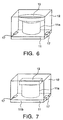
- the inductance component illustrated in Figs. 1 through 3 is adapted to be used as a magnetic device such as a transformer and an inductor.
- the inductance component comprises a magnetic core composed of first and second core members 11 and 12 faced to each other.
- the first core member 11 has a cylindrical leg portion 11a at its center.
- the second core member 12 has a flat or plate-like portion 12a faced to one end of the leg portion 11a through a magnetic gap t1.
- the first core member 11 further has a flange portion 11b radially outwardly expanding from the other end of the leg portion 11a.
- the second core member 12 further has a tubular portion 12b extending from an outer peripheral end of the plate-like portion 12a to surround the leg portion 11a and connected to the flange portion 11b.
- a disc-shaped permanent magnet 13 is fitted to the magnetic gap t1 of the magnetic core.
- an exciting coil 14 is arranged to surround the leg portion 11a.
- the permanent magnet 13 is arranged so that a magnetic field 16 generated by the permanent magnet 13 is opposite or reverse to a magnetic field 15 generated by the exciting coil 14.
- a terminal 17 is attached to an outer peripheral end of the flange portion 11b and connected to the exciting coil 14.
- the magnetic core used herein defines a magnetic path having a magnetic path length of 1.75 cm, an effective sectional area of 0.237 cm 2 , and a gap t1 of 230 ⁇ m.
- the exciting coil 14 has 10 turns and a d.c. resistance of 23 m ⁇ .
- the permanent magnet 13 has a thickness of 220 ⁇ m and a sectional area of 50.3 mm 2 . Thus, the permanent magnet 13 is greater in sectional area than the magnetic path of the magnetic core.
- preparation is made of an inductance component as a first comparative example which comprises a magnetic core having a middle leg portion 18 and a circular permanent magnet 19 having a sectional area of 23.8 mm 2 substantially similar to that of the middle leg portion 18.
- preparation is also made of an inductance component without using a permanent magnet.
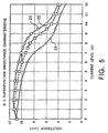
- d.c. superposition inductance characteristics are measured. The result is shown in Fig. 5.
- a solid line 21, a broken line 22, and a solid line 23 represent the d.c. superposition inductance characteristics of the inductance component in Figs. 1 through 3, the inductance component in Fig. 4, and the inductance component without using the magnetic bias, respectively.
- the inductance component in Figs. 1 through 3 is improved in d.c. superposition inductance characteristic by 23% or more as compared with the inductance component in Fig. 4.
- Fig. 6 a modification of the inductance component in Fig. 1 is shown.
- the permanent magnet 13 has a circular section while the middle leg portion 11a of the first core member 11 has a rectangular section.
- FIG. 7 and 8 description will be made of an inductance component according to a second embodiment of this invention. Parts similar in function to those of the inductance component illustrated in Figs. 1 through 3 are designated by like reference numerals and detailed description thereof will be omitted.
- the magnetic core used in this embodiment defines a magnetic path having a magnetic path length of 1.75 cm, an effective sectional area of 0.237 cm 2 , and a gap t2 of 230 ⁇ m.
- the exciting coil 14 has 10 turns and a d.c. resistance of 23 m ⁇ .
- the leg portion 11a of the first core member 11 has a circular section.
- the permanent magnet 13 has a thickness of 220 ⁇ m and a rectangular shape (square shape) with an area of 30.25 mm 2 .
- d.c. superposition inductance characteristics are measured.
- the result is shown in Fig. 9.
- a solid line 26, a broken line 27, and a solid line 28 represent the d.c. superposition inductance characteristics of the inductance component in Figs. 7 and 8, the inductance component in Fig. 4, and the inductance component without using the magnetic bias, respectively.
- the inductance component in Figs. 7 and 8 is improved in d.c. superposition inductance characteristic by 8% or more as compared with the inductance component in Fig. 4.
- the permanent magnet 13 since the permanent magnet 13 has a rectangular section, it is possible to effectively utilize the material as compared with the circular section.
- the permanent magnet 13 preferably comprises (1) at least one resin selected from polyamide imide resin, polyimide resin, epoxy resin, polyphenylene sulfide resin, silicone resin, polyester resin, aromatic polyamide resin, and liquid crystal polymer and (2) rare earth magnet powder dispersed therein, having an intrinsic coercive force of 796 k A/m (10 kOe) or more, Tc of 500°C or more, and an average particle size of 2.5-25 ⁇ m, and coated with at least one metal selected from Zn, Al, Bi, Ga, In, Mg, Pb, Sb, and Sn or alloy thereof.
- the resin has a content of 30% or more in volumetric ratio and a specific resistance of 0.1 ⁇ cm or more.
- the rare earth magnet powder preferably has a composition of Sm(Co bal. Fe 0.15-0.25 Cu 0.05-0.06 Zr 0.02-0.03 ) 7.0-8.5 .
- the rare earth magnet powder is coated with an inorganic glass having a softening point between 220°C and 550°C.
- the metal or the alloy coating the rare earth magnet powder is further coated with a nonmetallic inorganic compound having a melting point not lower than 300°C.
- the amount of the metal or the alloy, the inorganic glass, or a combination of the metal or the alloy and the nonmetallic inorganic compound preferably falls within a range between 0.1 and 10% in volume.
- the rare earth metal powder is oriented in a thickness direction in a magnetic field of 25T or more so that the permanent magnet is provided with magnetic anisotropy.
- the permanent magnet desirably has a center line average roughness of 10 ⁇ m or less.
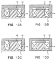
- each of the above-mentioned inductance component can be modified in various manners as illustrated in Figs. 10A through 10D. Parts having similar functions are designated by like reference numerals.
- the shape of the first and the second core members 11 and 12 as well as the shape and the size of the permanent magnet 13 can be modified in various manners.
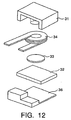
- the inductance component illustrated in Figs. 11 through 13 is also adapted to be used as a magnetic device such as a transformer and an inductor.
- the inductance component comprises a magnetic core composed of first and second core members 31 and 32 faced to each other.
- the first core member 31 comprises an E-shaped magnetic core having a cylindrical leg portion 31a at its center.
- the second core member 32 comprises an I-shaped magnetic core having a plate-like portion 32a faced to one end of the leg portion 31a through a magnetic gap.
- the first core member 31 further has a flange portion 31b radially outwardly expanding from the other end of the leg portion 31b and a pair of side plate portions 31c extending from opposite ends of the flange portion 31b in parallel to the leg portion 31a and connected to the plate-like portion 32a.
- a permanent magnet 33 is fitted to the magnetic gap.
- an exciting coil 34 is arranged to surround the leg portion 31a.
- the permanent magnet 33 is arranged so that a magnetic field 36 generated by the permanent magnet 33 is opposite or reverse to a magnetic field 35 generated by the exciting coil 34.
- the magnetic field 36 by the permanent magnet 33 and the magnetic field 35 by the exciting coil 34 are opposite to each other.
- An insulating base 36 is attached to the plate-like portion 32a.
- the insulating base 36 is a resin molded product.
- the exciting coil 34 has a portion 34a extending on or over the insulating base 36 to serve as a terminal known in the art.
- the first and the second core members 31 and 32 are made of Mn-Zn ferrite and define a magnetic path having a magnetic path length of 12.3 mm and an effective sectional area, i.e., a sectional area of the leg portion 31a, of 8.0 mm 2 .
- the magnetic path has a magnetic gap t3 equal to 200 ⁇ m.
- the permanent magnet 33 has a disc shape with a thickness of 150 ⁇ m and a diameter of 5mm. Therefore, the permanent magnet 33 is greater in sectional area than the magnetic path of the magnetic core.
- the exciting coil 34 has 3 turns.
- the leg portion 31a, the flange portion 31b, the side plate portions 31c, the plate-like portion 32a, the permanent magnet 33, and the exciting coil 34 correspond to the leg portion 11a, the flange portion 11b, the tubular portion 12b, the plate-like portion 12a, the permanent magnet 13, and the exciting coil 14, respectively. Therefore, the inductance component in Figs. 11 to 13 may be modified in the manner similar to those mentioned in conjunction with the first embodiment.
- an inductance component illustrated in Fig. 14 is prepared.
- the permanent magnet 33 is replaced by a permanent magnet 43 having an area (8.0 mm 2 ) equal to that of the leg portion 31 a of the inductance component in Figs. 11 to 13.
- the permanent magnet 43 is equal in thickness to the permanent magnet 33.
- an inductance component illustrated in Fig. 15 is.prepared.
- the inductance component illustrated in Fig. 15 has nothing equivalent or corresponding to the permanent magnet 33 of the inductance component in Figs. 11 to 13.
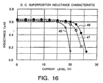
- d.c. superposition inductance characteristics are measured. The result is shown in Fig. 16.
- a solid line 46, a broken line 47, and a solid line 48 represent the d.c. superposition inductance characteristics of the inductance components in Figs. 11 to 13, Fig. 14, and Fig. 15, respectively.
- the inductance component in Figs. 11 to 13 is improved in d.c. superposition inductance characteristic by 25% or more as compared with the inductance component in Fig. 14.
Landscapes
- Engineering & Computer Science (AREA)
- Power Engineering (AREA)
- Chemical & Material Sciences (AREA)
- Composite Materials (AREA)
- Microelectronics & Electronic Packaging (AREA)
- Coils Or Transformers For Communication (AREA)
- Hard Magnetic Materials (AREA)
Description
- This invention relates to an inductance component which is a magnetic device such as a transformer and an inductor and, in particular, to an inductance component comprising a permanent magnet disposed in a magnetic gap formed in a magnetic core.
- In order to reduce the size and the weight of an inductance component, it is effective to reduce the volume of a magnetic core comprising a magnetic material. Generally, the magnetic core reduced in size easily reaches magnetic saturation so that a current level handled by a power supply is inevitably decreased. In order to solve the above-mentioned problem, there is known a technique in which the magnetic core is provided with a magnetic gap formed at a part thereof. With this structure, a magnetic resistance of the magnetic core is increased so that the decrease in current level is prevented. In this case, however, the magnetic core is decreased in magnetic inductance.
- In order to prevent the decrease in magnetic inductance, proposal is made of a technique related to such a structure that the magnetic core comprises a permanent magnet for generating a magnetic bias. In this technique, a d.c. magnetic bias is given to the magnetic core by the use of the permanent magnet. As a consequence, the number of magnetic lines of flux which can pass through the magnetic gap is increased.
- However, the existing inductance component using the permanent magnet is disadvantageous in the following respect. That is, the insertion amount or volume of the permanent magnet disposed in the magnetic gap is determined by a sectional area of a middle leg portion of the magnetic core and the dimension of the magnetic gap. Thus, the magnetic bias given to the magnetic core is inevitably restricted.
- The DE 29 51 513 A1 discloses an inductance element formed by a magnetic core which forms a magnetic circuit comprising a magnetic gap, a coil wound around the core, and a permanent magnet arranged in the gap.
- The abstract of the JP 11195541 published in the Patent Abstracts of Japan, October 29, 1999, describes an inductance element formed by a coil wound around a linear core, wherein permanent magnets are arranged at both sides of the linear core.
- The abstract of the JP 60010605 published in the Patent Abstracts of Japan, May 28, 1985, describes a permanent magnet for an inductance element. The magnet is composed of a rare earth magnetic powder bound with a resin.
- It is therefore an object of this invention to provide an inductance component capable of increasing the insertion amount of a permanent magnet to thereby obtain an appropriate magnetic biasing effect without varying the dimension of a magnetic gap.
- The object is attained by an inductance component according to
claim 1. Further developments of the invention are specified in the subordinate claims. -
- Fig. 1 is a perspective view of an inductance component according to a first embodiment of this invention with a part seen through;
- Fig. 2 is an exploded perspective view of the inductance component illustrated in Fig. 1;
- Fig. 3 is a side sectional view of the inductance component illustrated in Fig. 3;
- Fig. 4 is a perspective view of an inductance component as a first comparative example with a part seen through;
- Fig. 5 is a graph showing a d.c. superposition inductance characteristic of the inductance component illustrated in Fig. 1 in comparison with those of the first comparative example in Fig. 4 and another example without using a magnetic bias;
- Fig. 6 is a perspective view of a modification of the inductance component illustrated in Fig. 1 with a part seen through;
- Fig. 7 is a perspective view of an inductance component according to a second embodiment of this invention with a part seen through;
- Fig. 8 is a side sectional view of the inductance component illustrated in Fig. 7;
- Fig. 9 is a graph showing a d.c. superposition inductance characteristic of the inductance component illustrated in Fig. 7 in comparison with those of the first comparative example in Fig. 4 and another example without using a magnetic bias;
- Figs. 10A to 10D are side sectional views showing various modifications of the inductance component illustrated in Figs. 1 to 3;
- Fig. 11 is a perspective view of an inductance component according to a third embodiment of this invention;
- Fig. 12 is an exploded perspective view of the inductance component illustrated in Fig. 11;
- Fig. 13 is a side sectional view of the inductance component illustrated in Fig. 11;
- Fig. 14 is a side sectional view of an inductance component as a second comparative example;
- Fig. 15 is a side sectional view of an inductance component as a third comparative example; and
- Fig. 16 is a graph showing a d.c. superposition inductance characteristic of the inductance component illustrated in Fig. 11 in comparison with those of the second comparative example in Fig. 14 and the third comparative example in Fig. 15.
-
- Referring to Figs. 1 through 3, description will be made of an inductance component according to a first embodiment of this invention.
- The inductance component illustrated in Figs. 1 through 3 is adapted to be used as a magnetic device such as a transformer and an inductor. The inductance component comprises a magnetic core composed of first and
second core members first core member 11 has acylindrical leg portion 11a at its center. Thesecond core member 12 has a flat or plate-like portion 12a faced to one end of theleg portion 11a through a magnetic gap t1. Thefirst core member 11 further has aflange portion 11b radially outwardly expanding from the other end of theleg portion 11a. Thesecond core member 12 further has atubular portion 12b extending from an outer peripheral end of the plate-like portion 12a to surround theleg portion 11a and connected to theflange portion 11b. - To the magnetic gap t1 of the magnetic core, a disc-shaped
permanent magnet 13 is fitted. Between theleg portion 11a and thetubular portion 12b, anexciting coil 14 is arranged to surround theleg portion 11a. Thepermanent magnet 13 is arranged so that amagnetic field 16 generated by thepermanent magnet 13 is opposite or reverse to amagnetic field 15 generated by theexciting coil 14. Thus, themagnetic field 16 by thepermanent magnet 13 and themagnetic field 15 by theexciting coil 14 are opposite to each other. Aterminal 17 is attached to an outer peripheral end of theflange portion 11b and connected to theexciting coil 14. - The magnetic core used herein defines a magnetic path having a magnetic path length of 1.75 cm, an effective sectional area of 0.237 cm2, and a gap t1 of 230µm. The
exciting coil 14 has 10 turns and a d.c. resistance of 23 mΩ. Thepermanent magnet 13 has a thickness of 220µm and a sectional area of 50.3 mm2. Thus, thepermanent magnet 13 is greater in sectional area than the magnetic path of the magnetic core. - As illustrated in Fig. 4, preparation is made of an inductance component as a first comparative example which comprises a magnetic core having a
middle leg portion 18 and a circularpermanent magnet 19 having a sectional area of 23.8 mm2 substantially similar to that of themiddle leg portion 18. In addition, preparation is also made of an inductance component without using a permanent magnet. - For the inductance component in Figs. 1 through 3, the inductance component in Fig. 4, and the inductance component without using the magnetic bias, d.c. superposition inductance characteristics are measured. The result is shown in Fig. 5. In Fig. 5, a
solid line 21, abroken line 22, and asolid line 23 represent the d.c. superposition inductance characteristics of the inductance component in Figs. 1 through 3, the inductance component in Fig. 4, and the inductance component without using the magnetic bias, respectively. As is obvious from Fig. 5, the inductance component in Figs. 1 through 3 is improved in d.c. superposition inductance characteristic by 23% or more as compared with the inductance component in Fig. 4. - In Fig. 6, a modification of the inductance component in Fig. 1 is shown. As illustrated in the figure, the
permanent magnet 13 has a circular section while themiddle leg portion 11a of thefirst core member 11 has a rectangular section. - Referring to Figs. 7 and 8, description will be made of an inductance component according to a second embodiment of this invention. Parts similar in function to those of the inductance component illustrated in Figs. 1 through 3 are designated by like reference numerals and detailed description thereof will be omitted.
- The magnetic core used in this embodiment defines a magnetic path having a magnetic path length of 1.75 cm, an effective sectional area of 0.237 cm2, and a gap t2 of 230µm. The
exciting coil 14 has 10 turns and a d.c. resistance of 23 mΩ. Theleg portion 11a of thefirst core member 11 has a circular section. Thepermanent magnet 13 has a thickness of 220µm and a rectangular shape (square shape) with an area of 30.25 mm2. - For the inductance component in Figs. 7 and 8, the inductance component in Fig. 4, and the inductance component without using the magnetic bias, d.c. superposition inductance characteristics are measured. The result is shown in Fig. 9. In Fig. 9, a
solid line 26, a broken line 27, and asolid line 28 represent the d.c. superposition inductance characteristics of the inductance component in Figs. 7 and 8, the inductance component in Fig. 4, and the inductance component without using the magnetic bias, respectively. As is obvious from Fig. 9, the inductance component in Figs. 7 and 8 is improved in d.c. superposition inductance characteristic by 8% or more as compared with the inductance component in Fig. 4. Furthermore, since thepermanent magnet 13 has a rectangular section, it is possible to effectively utilize the material as compared with the circular section. - In each of the foregoing embodiment, the
permanent magnet 13 preferably comprises (1) at least one resin selected from polyamide imide resin, polyimide resin, epoxy resin, polyphenylene sulfide resin, silicone resin, polyester resin, aromatic polyamide resin, and liquid crystal polymer and (2) rare earth magnet powder dispersed therein, having an intrinsic coercive force of 796 k A/m (10 kOe) or more, Tc of 500°C or more, and an average particle size of 2.5-25 µm, and coated with at least one metal selected from Zn, Al, Bi, Ga, In, Mg, Pb, Sb, and Sn or alloy thereof. Preferably, the resin has a content of 30% or more in volumetric ratio and a specific resistance of 0.1 Ω cm or more. - The rare earth magnet powder preferably has a composition of Sm(Cobal.Fe0.15-0.25Cu0.05-0.06Zr0.02-0.03)7.0-8.5.
- Preferably, the rare earth magnet powder is coated with an inorganic glass having a softening point between 220°C and 550°C. Preferably, the metal or the alloy coating the rare earth magnet powder is further coated with a nonmetallic inorganic compound having a melting point not lower than 300°C. The amount of the metal or the alloy, the inorganic glass, or a combination of the metal or the alloy and the nonmetallic inorganic compound preferably falls within a range between 0.1 and 10% in volume.
- During production of the permanent magnet, the rare earth metal powder is oriented in a thickness direction in a magnetic field of 25T or more so that the permanent magnet is provided with magnetic anisotropy. The permanent magnet desirably has a center line average roughness of 10 µm or less.
- Each of the above-mentioned inductance component can be modified in various manners as illustrated in Figs. 10A through 10D. Parts having similar functions are designated by like reference numerals. Thus, the shape of the first and the
second core members permanent magnet 13 can be modified in various manners. - Referring to Figs. 11 through 13, description will be made of an inductance component according to a third embodiment of this invention.
- The inductance component illustrated in Figs. 11 through 13 is also adapted to be used as a magnetic device such as a transformer and an inductor. The inductance component comprises a magnetic core composed of first and
second core members first core member 31 comprises an E-shaped magnetic core having acylindrical leg portion 31a at its center. Thesecond core member 32 comprises an I-shaped magnetic core having a plate-like portion 32a faced to one end of theleg portion 31a through a magnetic gap. Thefirst core member 31 further has aflange portion 31b radially outwardly expanding from the other end of theleg portion 31b and a pair ofside plate portions 31c extending from opposite ends of theflange portion 31b in parallel to theleg portion 31a and connected to the plate-like portion 32a. - To the magnetic gap, a
permanent magnet 33 is fitted. Between theleg portion 31a and theside plate portions 31c, anexciting coil 34 is arranged to surround theleg portion 31a. Thepermanent magnet 33 is arranged so that amagnetic field 36 generated by thepermanent magnet 33 is opposite or reverse to amagnetic field 35 generated by theexciting coil 34. Thus, themagnetic field 36 by thepermanent magnet 33 and themagnetic field 35 by theexciting coil 34 are opposite to each other. - An insulating
base 36 is attached to the plate-like portion 32a. The insulatingbase 36 is a resin molded product. Theexciting coil 34 has aportion 34a extending on or over the insulatingbase 36 to serve as a terminal known in the art. - The first and the
second core members leg portion 31a, of 8.0 mm2. The magnetic path has a magnetic gap t3 equal to 200µm. Thepermanent magnet 33 has a disc shape with a thickness of 150µm and a diameter of 5mm. Therefore, thepermanent magnet 33 is greater in sectional area than the magnetic path of the magnetic core. Theexciting coil 34 has 3 turns. - Comparison will be made between the inductance component in Figs. 11 to 13 and the inductance component in Figs. 1 to 3. The
leg portion 31a, theflange portion 31b, theside plate portions 31c, the plate-like portion 32a, thepermanent magnet 33, and theexciting coil 34 correspond to theleg portion 11a, theflange portion 11b, thetubular portion 12b, the plate-like portion 12a, thepermanent magnet 13, and theexciting coil 14, respectively. Therefore, the inductance component in Figs. 11 to 13 may be modified in the manner similar to those mentioned in conjunction with the first embodiment. - As a second comparative example, an inductance component illustrated in Fig. 14 is prepared. In the inductance component in Fig. 14, the
permanent magnet 33 is replaced by apermanent magnet 43 having an area (8.0 mm2) equal to that of theleg portion 31 a of the inductance component in Figs. 11 to 13. Thepermanent magnet 43 is equal in thickness to thepermanent magnet 33. - As a third comparative example, an inductance component illustrated in Fig. 15 is.prepared. The inductance component illustrated in Fig. 15 has nothing equivalent or corresponding to the
permanent magnet 33 of the inductance component in Figs. 11 to 13. - For the inductance components in Figs. 11 to 13, Fig. 14, and Fig. 15, d.c. superposition inductance characteristics are measured. The result is shown in Fig. 16. In Fig. 16, a
solid line 46, a broken line 47, and asolid line 48 represent the d.c. superposition inductance characteristics of the inductance components in Figs. 11 to 13, Fig. 14, and Fig. 15, respectively. As is obvious from Fig. 16, the inductance component in Figs. 11 to 13 is improved in d.c. superposition inductance characteristic by 25% or more as compared with the inductance component in Fig. 14.
Claims (15)
- An inductance component comprising:wherein said permanent magnet comprises:a magnetic core forming a magnetic circuit having a magnetic gap;an exciting coil wound around said magnetic core; anda permanent magnet disposed in said magnetic gap and greater in sectional area than said magnetic core,at least one resin selected from polyamide imide resin, polyimide resin, epoxy resin, polyphenylene sulfide resin, silicone resin, polyester resin, aromatic polyamide resin, and liquid crystal polymer; andrare earth magnet powder dispersed in said at least one resin, having an intrinsic coercive force of 796 k A/m (10 kOe) or more, Tc of 500°C or more, and an average particle size of 2.5-25µm, and coated with at least one metal selected from Zn, Al, Bi, Ga, In, Mg, Pb, Sb, and Sn or alloy thereof, the resin having a content of 30% or more in volumetric ratio and a specific resistance of 0.1 Ωcm or more.
- The inductance component according to claim 1, wherein said rare earth magnet powder has a composition of Sm(Cobal.Fe0.15-0.25Cu0.05-0.06Zr0.02. 0.03)7.0-8.5.
- The inductance component according to claim 1 or 2, wherein said rare earth magnet powder is coated with an inorganic glass having a softening point between 220°C and 550°C.
- The inductance component according to one of claims 1 to 3, wherein said metal or said alloy coating said rare earth magnet powder is further coated with a nonmetallic inorganic compound having a melting point not lower than 300°C.
- The inductance component according to one of claims 1 to 4, wherein the amount of said metal or said alloy, said inorganic glass, or a combination of said metal or said alloy and said nonmetallic inorganic compound falls within a range between 0.1 and 10%.
- The inductance component according to one of claims 1 to 5, wherein said rare earth magnet powder is oriented in a magnetic field applied during production of said permanent magnet so that said permanent magnet is provided with magnetic anisotropy.
- The inductance component according to one of claims 1 to 6, wherein said permanent magnet is magnetized in a magnetic field of 25T or more.
- The inductance component according to one of claims 1 to 7, wherein said permanent magnet has a center line average roughness of 10µm or less.
- The inductance component according to one of claims 1 to 8, wherein said magnetic core comprises first and second core members faced to each other, said first core member having a leg portion, said second core member having a plate-like portion faced to one end of said leg portion through said magnetic gap.
- The inductance component according to claim 9, wherein said first core member further has a flange portion radially outwardly expanding from the other end of said leg portion, said second core portion further having a tubular portion extending from an outer peripheral end of said plate-like portion to surround said leg portion and connected to said flange portion.
- The inductance component according to claim 10, wherein said exciting coil is arranged between said leg portion and said tubular portion to surround said leg portion.
- The inductance component according to claim 10 or 11, further comprising a terminal attached to an outer peripheral end of said flange portion and connected to said exciting coil.
- The inductance component according to one of claims 9 to 12, wherein said first core member has a flange portion radially outwardly expanding from the other end of said leg portion and a side plate portion extending from an outer peripheral end of said flange portion in parallel to said leg portion and connected to said plate-like portion.
- The inductance component according to claim 13, wherein said exciting coil is arranged between said leg portion and said side plate portion to surround said leg portion.
- The inductance component according to one of claims 9 to 14, further comprising an insulating base attached to said plate-like portion, said exciting coil has a portion extending over said insulating base to serve as a terminal.
Applications Claiming Priority (2)
| Application Number | Priority Date | Filing Date | Title |
|---|---|---|---|
| JP2001163302A JP2002359126A (en) | 2001-05-30 | 2001-05-30 | Inductance component |
| JP2001163302 | 2001-05-30 |
Publications (2)
| Publication Number | Publication Date |
|---|---|
| EP1263005A1 EP1263005A1 (en) | 2002-12-04 |
| EP1263005B1 true EP1263005B1 (en) | 2004-11-17 |
Family
ID=19006301
Family Applications (1)
| Application Number | Title | Priority Date | Filing Date |
|---|---|---|---|
| EP02011979A Expired - Lifetime EP1263005B1 (en) | 2001-05-30 | 2002-05-29 | Inductance component comprising a permanent magnet greater in sectional area than a magnetic path and disposed in a magnetic gap |
Country Status (5)
| Country | Link |
|---|---|
| US (1) | US6791446B2 (en) |
| EP (1) | EP1263005B1 (en) |
| JP (1) | JP2002359126A (en) |
| CN (1) | CN1433033A (en) |
| DE (1) | DE60201941T2 (en) |
Families Citing this family (11)
| Publication number | Priority date | Publication date | Assignee | Title |
|---|---|---|---|---|
| DE10259117A1 (en) * | 2002-12-18 | 2004-07-01 | Technische Universität Ilmenau Abteilung Forschungsförderung und Technologietransfer | Inductive component to be magnetically compensated in ferromagnetic circuit has coil and magnetic circuit made from ferromagnetic material |
| TWI274220B (en) * | 2003-08-19 | 2007-02-21 | Hannstar Display Corp | A liquid crystal display having thin cell gap and method of producing the same |
| TWI315529B (en) * | 2006-12-28 | 2009-10-01 | Ind Tech Res Inst | Monolithic inductor |
| CN101325122B (en) * | 2007-06-15 | 2013-06-26 | 库帕技术公司 | Miniature Shielded Magnetics |
| FI122086B (en) * | 2007-07-06 | 2011-08-15 | Vacon Oyj | Filterdrosselarrangemang |
| TWI438792B (en) * | 2011-01-04 | 2014-05-21 | Cyntec Co Ltd | Inductor |
| CN102568768A (en) * | 2012-02-22 | 2012-07-11 | 临沂中瑞电子有限公司 | Fixed inductance magnetic core for LED (light emitting diode) |
| CN103824675A (en) * | 2013-12-31 | 2014-05-28 | 芜湖国睿兆伏电子有限公司 | Adjustable inductor |
| JP6237269B2 (en) * | 2014-01-28 | 2017-11-29 | Tdk株式会社 | Reactor |
| US10210983B2 (en) * | 2015-06-17 | 2019-02-19 | Abb Schweiz Ag | Electromagnetic induction device |
| JP2017069460A (en) * | 2015-09-30 | 2017-04-06 | 太陽誘電株式会社 | Coil component and manufacturing method therefor |
Family Cites Families (10)
| Publication number | Priority date | Publication date | Assignee | Title |
|---|---|---|---|---|
| DE2951313A1 (en) | 1979-12-20 | 1981-07-02 | Vogt Gmbh & Co Kg, 8391 Erlau | Beam deflection current linearising coil for TV receiver - has ferrite case to limit stray flux from permanent magnet |
| JPS6010605A (en) * | 1983-06-30 | 1985-01-19 | Hitachi Metals Ltd | Permanent magnet for inductance element |
| JPS62234302A (en) * | 1985-10-30 | 1987-10-14 | Kanegafuchi Chem Ind Co Ltd | Fireretardant resin magnet |
| EP0452580B1 (en) * | 1990-04-19 | 1999-06-23 | Seiko Epson Corporation | A resin bound magnet and its production process |
| JP2981702B2 (en) * | 1992-08-27 | 1999-11-22 | 愛三工業株式会社 | Ignition coil for internal combustion engine |
| JP3230647B2 (en) | 1994-12-09 | 2001-11-19 | 株式会社安川電機 | DC reactor |
| JP3007561B2 (en) * | 1995-10-05 | 2000-02-07 | 信越化学工業株式会社 | Method of joining R-Fe-B permanent magnet and yoke |
| JP3647995B2 (en) * | 1996-11-06 | 2005-05-18 | 株式会社三徳 | Powder for permanent magnet, method for producing the same and anisotropic permanent magnet using the powder |
| JP3537635B2 (en) * | 1997-05-28 | 2004-06-14 | 京セラ株式会社 | Wound inductor |
| JP3263022B2 (en) * | 1998-01-06 | 2002-03-04 | エフ・ディ−・ケイ株式会社 | Linearity coil |
-
2001
- 2001-05-30 JP JP2001163302A patent/JP2002359126A/en not_active Withdrawn
-
2002
- 2002-05-29 DE DE60201941T patent/DE60201941T2/en not_active Expired - Lifetime
- 2002-05-29 EP EP02011979A patent/EP1263005B1/en not_active Expired - Lifetime
- 2002-05-29 US US10/157,697 patent/US6791446B2/en not_active Expired - Lifetime
- 2002-05-30 CN CN02141351A patent/CN1433033A/en active Pending
Also Published As
| Publication number | Publication date |
|---|---|
| JP2002359126A (en) | 2002-12-13 |
| US20020180575A1 (en) | 2002-12-05 |
| DE60201941D1 (en) | 2004-12-23 |
| US6791446B2 (en) | 2004-09-14 |
| EP1263005A1 (en) | 2002-12-04 |
| DE60201941T2 (en) | 2005-11-03 |
| CN1433033A (en) | 2003-07-30 |
Similar Documents
| Publication | Publication Date | Title |
|---|---|---|
| US6710693B2 (en) | Inductor component containing permanent magnet for magnetic bias and method of manufacturing the same | |
| EP1263005B1 (en) | Inductance component comprising a permanent magnet greater in sectional area than a magnetic path and disposed in a magnetic gap | |
| KR20040107409A (en) | Magnetic core and coil component using the same | |
| US7915993B2 (en) | Inductor | |
| KR20020042516A (en) | Magnetic core including magnet for magnetic bias and inductor component using the same | |
| KR20030025307A (en) | Permanent magnet, magnetic core having the magnet as bias magnet, and inductance parts using the core | |
| US6734771B2 (en) | Inductor component having a permanent magnet in the vicinity of magnetic gap | |
| EP1225601B1 (en) | Inductor component | |
| EP1178501B1 (en) | Inductance component having a permanent magnet in the vicinity of a magnetic gap | |
| US6545582B2 (en) | Magnetic core having an effective magnetic bias and magnetic device using the magnetic core | |
| JP2002222707A (en) | Inductance component | |
| JP4623818B2 (en) | Inductor | |
| JP2002359125A (en) | Inductor component | |
| JP3974773B2 (en) | Magnetic core having magnet for magnetic bias and inductance component using the same | |
| JP2002222714A (en) | Inductor | |
| JP2002289443A (en) | Inductor component | |
| JP2002222721A (en) | Inductor | |
| JP2002158116A (en) | Inductor | |
| JP2003017340A (en) | Inductor component | |
| JP2006245418A (en) | Inductance component | |
| JP2002217042A (en) | Inductance component and manufacturing method thereof | |
| JP2002170719A (en) | Inductance part | |
| HK1042984A (en) | Inductance component having a permanent magnet in the vicinity of a magnetic gap | |
| HK1148384A (en) | High power inductors using a magnetic bias | |
| JP2005011992A (en) | Magnetic core and inductance component using it |
Legal Events
| Date | Code | Title | Description |
|---|---|---|---|
| PUAI | Public reference made under article 153(3) epc to a published international application that has entered the european phase |
Free format text: ORIGINAL CODE: 0009012 |
|
| AK | Designated contracting states |
Kind code of ref document: A1 Designated state(s): AT BE CH CY DE DK ES FI FR GB GR IE IT LI LU MC NL PT SE TR |
|
| AX | Request for extension of the european patent |
Free format text: AL;LT;LV;MK;RO;SI |
|
| 17P | Request for examination filed |
Effective date: 20030523 |
|
| AKX | Designation fees paid |
Designated state(s): DE FR GB |
|
| 17Q | First examination report despatched |
Effective date: 20030723 |
|
| GRAP | Despatch of communication of intention to grant a patent |
Free format text: ORIGINAL CODE: EPIDOSNIGR1 |
|
| GRAS | Grant fee paid |
Free format text: ORIGINAL CODE: EPIDOSNIGR3 |
|
| GRAA | (expected) grant |
Free format text: ORIGINAL CODE: 0009210 |
|
| AK | Designated contracting states |
Kind code of ref document: B1 Designated state(s): DE FR GB |
|
| REG | Reference to a national code |
Ref country code: GB Ref legal event code: FG4D |
|
| REG | Reference to a national code |
Ref country code: IE Ref legal event code: FG4D |
|
| REF | Corresponds to: |
Ref document number: 60201941 Country of ref document: DE Date of ref document: 20041223 Kind code of ref document: P |
|
| PLBE | No opposition filed within time limit |
Free format text: ORIGINAL CODE: 0009261 |
|
| STAA | Information on the status of an ep patent application or granted ep patent |
Free format text: STATUS: NO OPPOSITION FILED WITHIN TIME LIMIT |
|
| 26N | No opposition filed |
Effective date: 20050818 |
|
| ET | Fr: translation filed | ||
| PG25 | Lapsed in a contracting state [announced via postgrant information from national office to epo] |
Ref country code: GB Free format text: LAPSE BECAUSE OF NON-PAYMENT OF DUE FEES Effective date: 20060529 |
|
| GBPC | Gb: european patent ceased through non-payment of renewal fee |
Effective date: 20060529 |
|
| PG25 | Lapsed in a contracting state [announced via postgrant information from national office to epo] |
Ref country code: FR Free format text: LAPSE BECAUSE OF NON-PAYMENT OF DUE FEES Effective date: 20050531 |
|
| PGFP | Annual fee paid to national office [announced via postgrant information from national office to epo] |
Ref country code: DE Payment date: 20100526 Year of fee payment: 9 |
|
| REG | Reference to a national code |
Ref country code: FR Ref legal event code: ST Effective date: 20100730 |
|
| REG | Reference to a national code |
Ref country code: DE Ref legal event code: R119 Ref document number: 60201941 Country of ref document: DE Effective date: 20111201 |
|
| PG25 | Lapsed in a contracting state [announced via postgrant information from national office to epo] |
Ref country code: DE Free format text: LAPSE BECAUSE OF NON-PAYMENT OF DUE FEES Effective date: 20111201 |