EP1261242A1 - Method for manufacturing circuit board - Google Patents
Method for manufacturing circuit board Download PDFInfo
- Publication number
- EP1261242A1 EP1261242A1 EP01981091A EP01981091A EP1261242A1 EP 1261242 A1 EP1261242 A1 EP 1261242A1 EP 01981091 A EP01981091 A EP 01981091A EP 01981091 A EP01981091 A EP 01981091A EP 1261242 A1 EP1261242 A1 EP 1261242A1
- Authority
- EP
- European Patent Office
- Prior art keywords
- metal plate
- circuit board
- manufacturing circuit
- hard coat
- coat layer
- Prior art date
- Legal status (The legal status is an assumption and is not a legal conclusion. Google has not performed a legal analysis and makes no representation as to the accuracy of the status listed.)
- Withdrawn
Links
Images



Classifications
-
- C—CHEMISTRY; METALLURGY
- C23—COATING METALLIC MATERIAL; COATING MATERIAL WITH METALLIC MATERIAL; CHEMICAL SURFACE TREATMENT; DIFFUSION TREATMENT OF METALLIC MATERIAL; COATING BY VACUUM EVAPORATION, BY SPUTTERING, BY ION IMPLANTATION OR BY CHEMICAL VAPOUR DEPOSITION, IN GENERAL; INHIBITING CORROSION OF METALLIC MATERIAL OR INCRUSTATION IN GENERAL
- C23C—COATING METALLIC MATERIAL; COATING MATERIAL WITH METALLIC MATERIAL; SURFACE TREATMENT OF METALLIC MATERIAL BY DIFFUSION INTO THE SURFACE, BY CHEMICAL CONVERSION OR SUBSTITUTION; COATING BY VACUUM EVAPORATION, BY SPUTTERING, BY ION IMPLANTATION OR BY CHEMICAL VAPOUR DEPOSITION, IN GENERAL
- C23C8/00—Solid state diffusion of only non-metal elements into metallic material surfaces; Chemical surface treatment of metallic material by reaction of the surface with a reactive gas, leaving reaction products of surface material in the coating, e.g. conversion coatings, passivation of metals
- C23C8/06—Solid state diffusion of only non-metal elements into metallic material surfaces; Chemical surface treatment of metallic material by reaction of the surface with a reactive gas, leaving reaction products of surface material in the coating, e.g. conversion coatings, passivation of metals using gases
- C23C8/08—Solid state diffusion of only non-metal elements into metallic material surfaces; Chemical surface treatment of metallic material by reaction of the surface with a reactive gas, leaving reaction products of surface material in the coating, e.g. conversion coatings, passivation of metals using gases only one element being applied
- C23C8/24—Nitriding
- C23C8/26—Nitriding of ferrous surfaces
-
- B—PERFORMING OPERATIONS; TRANSPORTING
- B30—PRESSES
- B30B—PRESSES IN GENERAL
- B30B15/00—Details of, or accessories for, presses; Auxiliary measures in connection with pressing
- B30B15/06—Platens or press rams
- B30B15/062—Press plates
-
- B—PERFORMING OPERATIONS; TRANSPORTING
- B32—LAYERED PRODUCTS
- B32B—LAYERED PRODUCTS, i.e. PRODUCTS BUILT-UP OF STRATA OF FLAT OR NON-FLAT, e.g. CELLULAR OR HONEYCOMB, FORM
- B32B15/00—Layered products comprising a layer of metal
- B32B15/04—Layered products comprising a layer of metal comprising metal as the main or only constituent of a layer, which is next to another layer of the same or of a different material
- B32B15/08—Layered products comprising a layer of metal comprising metal as the main or only constituent of a layer, which is next to another layer of the same or of a different material of synthetic resin
-
- B—PERFORMING OPERATIONS; TRANSPORTING
- B32—LAYERED PRODUCTS
- B32B—LAYERED PRODUCTS, i.e. PRODUCTS BUILT-UP OF STRATA OF FLAT OR NON-FLAT, e.g. CELLULAR OR HONEYCOMB, FORM
- B32B5/00—Layered products characterised by the non- homogeneity or physical structure, i.e. comprising a fibrous, filamentary, particulate or foam layer; Layered products characterised by having a layer differing constitutionally or physically in different parts
- B32B5/02—Layered products characterised by the non- homogeneity or physical structure, i.e. comprising a fibrous, filamentary, particulate or foam layer; Layered products characterised by having a layer differing constitutionally or physically in different parts characterised by structural features of a fibrous or filamentary layer
-
- C—CHEMISTRY; METALLURGY
- C23—COATING METALLIC MATERIAL; COATING MATERIAL WITH METALLIC MATERIAL; CHEMICAL SURFACE TREATMENT; DIFFUSION TREATMENT OF METALLIC MATERIAL; COATING BY VACUUM EVAPORATION, BY SPUTTERING, BY ION IMPLANTATION OR BY CHEMICAL VAPOUR DEPOSITION, IN GENERAL; INHIBITING CORROSION OF METALLIC MATERIAL OR INCRUSTATION IN GENERAL
- C23C—COATING METALLIC MATERIAL; COATING MATERIAL WITH METALLIC MATERIAL; SURFACE TREATMENT OF METALLIC MATERIAL BY DIFFUSION INTO THE SURFACE, BY CHEMICAL CONVERSION OR SUBSTITUTION; COATING BY VACUUM EVAPORATION, BY SPUTTERING, BY ION IMPLANTATION OR BY CHEMICAL VAPOUR DEPOSITION, IN GENERAL
- C23C8/00—Solid state diffusion of only non-metal elements into metallic material surfaces; Chemical surface treatment of metallic material by reaction of the surface with a reactive gas, leaving reaction products of surface material in the coating, e.g. conversion coatings, passivation of metals
- C23C8/02—Pretreatment of the material to be coated
-
- H—ELECTRICITY
- H05—ELECTRIC TECHNIQUES NOT OTHERWISE PROVIDED FOR
- H05K—PRINTED CIRCUITS; CASINGS OR CONSTRUCTIONAL DETAILS OF ELECTRIC APPARATUS; MANUFACTURE OF ASSEMBLAGES OF ELECTRICAL COMPONENTS
- H05K3/00—Apparatus or processes for manufacturing printed circuits
- H05K3/02—Apparatus or processes for manufacturing printed circuits in which the conductive material is applied to the surface of the insulating support and is thereafter removed from such areas of the surface which are not intended for current conducting or shielding
- H05K3/022—Processes for manufacturing precursors of printed circuits, i.e. copper-clad substrates
-
- H—ELECTRICITY
- H05—ELECTRIC TECHNIQUES NOT OTHERWISE PROVIDED FOR
- H05K—PRINTED CIRCUITS; CASINGS OR CONSTRUCTIONAL DETAILS OF ELECTRIC APPARATUS; MANUFACTURE OF ASSEMBLAGES OF ELECTRICAL COMPONENTS
- H05K3/00—Apparatus or processes for manufacturing printed circuits
- H05K3/40—Forming printed elements for providing electric connections to or between printed circuits
- H05K3/4038—Through-connections; Vertical interconnect access [VIA] connections
- H05K3/4053—Through-connections; Vertical interconnect access [VIA] connections by thick-film techniques
- H05K3/4069—Through-connections; Vertical interconnect access [VIA] connections by thick-film techniques for via connections in organic insulating substrates
Definitions
- the present invention relates to a method of manufacturing a circuit board.
- the method comprises: sandwiching a B stage prepreg sheet made by impregnating woven or non-woven fabric made of glass fiber or aramid fiber with thermosetting resin between two sheets of copper foils; further sandwiching the sandwiched laminate between metal plates disposed top and bottom; heat press the further sandwiched laminate to forming a unitary laminate; and forming a desired circuit pattern by etching the copper foils to obtain a circuit board.
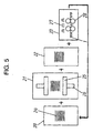
- Fig. 5 is a schematic diagram of a conventional circuit board manufacturing method using a hot press as a major unit. First, prepreg sheet held between metal foils and further sandwiched between metal plates at a top and bottom thereof, or laminate 24, is placed in assembly unit 20.
- the laminate 24 is usually stacked with a few or more than 10 laminates, each comprising board material and copper foils sandwiched between metal plates disposed on top and bottom thereof, to improve the productivity.
- the laminate 24 is moved into hot press unit 21 and is placed between top and bottom hot platens 25 to be heated and pressed. Inside the hot platens 25 is disposed hot oil or steam piping for heating the laminate 24.
- hydraulic cylinder 26 is supplied with high pressure oil to apply an appropriate pressure to the laminate 24.
- the heating and pressing process is usually called a heat press process, where B-stage resin in the prepreg sheet melts and cures to adher the copper foils, to be formed into a shape as a circuit board.
- the laminate 24 is moved to disassembly unit 22 and is separated into metal plate and board material with copper foil adhered thereto.
- the board material is delivered to the circuit forming process for forming the desired circuit, and the metal plate is delivered to and cleaned at cleaning device 23 and then to the re-assembly unit to be sequentially used in the next heat press process.
- the main role of the cleaning device 23 is to scribe away the sticking resin from the metal plate surface and to smoothen the metal plate surface by removing scratches or projections therefrom, thereby keeping the metal plate surface clean at all times.
- the cleaning device 23 is, as shown in the figure, provided with a water shower 27 and rotary polishing buff 28, which polishes and cleans the surfaces of metal plates sequentially passed through.
- the polishing buff 28 is a brush or roll-form wheel made of synthetic fiber or the like with abrasive grain bonded to the surface thereof and serves to remove sticking matter while polishing the metal plate surface.
- the grade of polishing buff is expressed by grain number, and when used for metal plate cleaning, those ranging from 300 to 600 are usually employed.
- the polishing operation grinds and removes not only the contamination but also the surface of the metal plate as well, the metal plate is reduced in thickness through repetition of polishing operation and becomes unable to be used for the production of the circuit board, then it is necessary to replace the metal plate with new one.
- circuit board manufactured will become uneven in thickness as a matter of course.
- the method of manufacturing circuit board of the present invention includes a heat press process in which a laminate with metal foil(s) disposed on both surfaces or on one surface of a board material made of at least one kind of material or a board material with metal foil circuit formed thereon is placed between metal plates and subjected to a heat press process at least under heat or pressure, wherein a hard coat layer is formed on both surfaces or one surface of the metal plates.
- the metal plate is protected by the hard coat layer, the metal plate is hardly scratched by a contact with the conveyor and the like or by the operator's handling during the production of the circuit boards. Further, finishing of the surface of the hard coat layer as smooth as possible makes it possible to easily remove resin or contamination sticking to the metal plate, to lessen the abrasion of the metal plate even when the conventional polishing method is applied, and to prolong the life of the metal plate. As a result, it is possible to produce the high-quality circuit boards at low costs.
- Fig. 1 is a sectional view of a metal plate used in a method of manufacturing a circuit board in the first preferred embodiment of the present invention.
- hard coat layer 2 is formed on both surfaces of a metal plate 1 made of stainless steel having a thickness of 1 mm.
- the hard coat layer 2 is formed by using a so-called nitriding process wherein nitrogen atom is diffused into the stainless steel surface.
- a wet process such as a salt bath method or the like is also well known as a nitriding process, but a gas nitriding process is employed in the present preferred embodiment.
- a gas nitriding process is a preferable treatment method since the hard coat layer 2 is required to have a dense structure and an internal uniformity as well as a hardness.
- a fluoride layer is formed on the metal plate surface by heating the metal plate in a gas containing NF 3 before nitriding treatment, then, the metal plate 1 is heated in a gas containing NH 3 to form a nitride layer on the metal plate surface.
- the layer thickness of the hard coat layer 2 is preferably to be 10 ⁇ m or more in the production of the circuit boards, though, it depends upon the structure of the hard coat layer 2 and a material quality of the metal plate 1.
- the layer thickness is preferably to be less than 100 ⁇ m, and more preferable to be less than 50 ⁇ m.
- the surface roughness (JIS B0601) of the hard layer 2 is preferable to have an average surface roughness Ra of 0.1 ⁇ m or less and maximum surface roughness Rmax of 2 ⁇ m or less, and more preferably, Ra of 0.05 ⁇ m or less and Rmax of 1 ⁇ m or less.
- polishing means such as a polishing buff or brush of grain size of #700 or more.
- the particle diameter of a grain used for a polishing means of No. 700 or like is usually about 30 ⁇ m, and in order to make use of the advantage of the present invention, a metal plate surface that is extremely excellent in surface smoothness can be obtained by using a polishing means of grain size of #1000 or more.
- the above surface finishing conditions can be freely selected according to the type of circuit board obtained, the production cost, productivity and the like. Further, as for the metal plate surface polishing conditions, it is also possible to obtain a surface smoothness by executing similar finish polishing to the surface of the hard coat layer 2.
- the hard coat layer 2 is abrasion-resistant and poor in polishing workability, it is efficient to polish the metal plate 1 up to the desired smoothness before hard coat layer forming, and, after forming hard coat layer, to polish a slight amount to obtain the desired smoothness.
- Fig. 2A through Fig. 2F are sectional views of a process, showing the circuit board manufacturing method in the second preferred embodiment of the present invention.
- films 4 is temporarily pressed by a roll laminating method or the like onto a board material 3 formed of prepreg sheet whose reinforce material is impregnated with B-stage thermosetting resin. Then, through-holes 5 are formed in the board material by a drilling means using a laser beam.
- aramid fiber non-woven fabric is used as a reinforce material
- a thickness of the board material 3 is about 130 ⁇ m
- a diameter of the through-hole 5 is about 150 ⁇ m
- a thickness of the film 4 is about 20 ⁇ m.
- the film 4 is peeled off as shown in Fig. 2C to obtain an intermediate material where the conductive paste 6 is slightly protruded from the board material 3.
- metal plates 1 with hard layers 2 formed thereon, copper foils 7 of 15 m in thickness, and the intermediate material are laminated and then heat pressed in the a heat press process, thereby obtaining a double-sided copper clad laminate as shown in Fig. 2E.
- the thickness of the copper foil is not limited to 15 ⁇ m, but less expensive copper foil of 35 ⁇ m in thickness can be used when fine wiring is not required.
- copper foil of 8 ⁇ m or less in thickness, 3 ⁇ m for example, can be used.
- the present invention is suited for a high precision circuit board using thin foils in particular.
- the conditions for the heat press process are a 3-hour program including the temperature rise and temperature fall with one hour keeping at 180 °C peak temperature, and 300N pressure applied per one square centimeter.
- the board material 3 is compressed in the heat press process and becomes about 110 ⁇ m in thickness.
- the conductive paste 6 is compressed in the direction of thickness of board material 3, then the copper foils 7 on either surface of the board material are electrically connected to each other.
- copper foils 7 are selectively etched to form circuit patterns, and thereby, a circuit board 9 with circuit patterns 8 formed on either surface thereof can be obtained as shown in Fig. 2F.
- copper foils of 20 ⁇ m or less in thickness are used as the metal foil, but it is also possible to use copper foils with a different material coated on the surface thereof or metal foils other than copper foils.
- the hard coat layer 2 is formed on the surface of the metal plate 1, and moreover, the surface is smoothly finished, it is possible to apply pressures without damaging the copper foil 7 in the heat press process. Particularly; when a surface of the copper foil 7 is roughened, little damage will be given to the surface.
- efficient compressing of the conductive paste 6 is a inevitable condition for reliably forming the electrical connection of the circuit board.
- a mechanical rigidity of the metal plate 1 is considerably enhanced due to the effect of the hard coat layer 2, and the deformation of metal plate 1 is very little during compression, it is possible to effectively compress the conductive paste 6.
- the thickness of hard layer 2 is preferable to be 10 ⁇ m or more, and the surface of hard coat layer 2 is preferable to have 500 HV or more in Vickers hardness, and also, the hardness of the metal plate 1 itself is preferable to be 300 HV or more.
- the metal plate 1 is also subjected to a surface cleaning by a cleaning device after the heat press process the same as in a conventional circuit board manufacturing method. But, it is very easy to remove contamination or sticking matter due to the effect of the hard coat layer 2 that is the feature of the present invention. Accordingly, sticking matter can be easily removed by slightly rubbing the surface with a polishing buff of #1000 or more.
- the thickness of the metal plate 1 hardly changes after being passed a plurality of times through the cleaning device.
- Fig. 3 shows the change in thickness of the metal plate 1 including the hard coat layer 2 when the metal plate 1 has been passed through the cleaning device up to 500 times.
- the rate of change in plate thickness varies with the condition setting or the like of the metal plate cleaning device.
- a stainless steel plate of 1 mm thick and having hard coat layers 2 of 15 ⁇ m thick formed by nitriding treatment is passed through a cleaning device using a polishing buff of #1000, the plate thickness is changed by about 2 ⁇ m after 500 times of the polishing.
- the amount of abrasion due to the polishing is 1 ⁇ m on each surface. From this result, in a simplified calculation, when a hard coat layer of 15 ⁇ m is formed, the entire hard layer wears out after 75,000 times of polishing, meaning the termination of its life. However, as a result of the inventor's experiment, the hard coat layer was able to endure at least more than 10,000 times of polishing.
- Shown in Fig. 3 is an comparative example of change in plate thickness when stainless steel plate (surface hardness: 350 HV) of 1 mm thick not provided with hard coat layer and used in a conventional circuit board manufacturing method is passed through a cleaning device using a polishing buff of #320, where the plate is reduced in thickness by about 200 ⁇ m after 500 times of polishing.
- stainless steel plate surface hardness: 350 HV
- polishing buff of grain No. of #600 or more is used to suppress the reduction in plate thickness, it will result in lowering of the polishing ability and become unable to remove contamination such as resin sticking to the metal plate surface.
- the metal plate surface is hardly scratched and also can be kept clean since a hard coat layer is formed on the surface of the metal plate. Accordingly, it is possible to produce a high quality circuit board by using the metal plate of the present invention.
- a double-sided circuit board is described in the present preferred embodiment, but it is possible to manufacture a multi-layered circuit board by the process described above, with a double-sided circuit board or multi-layered circuit board disposed at the middle and with prepreg sheets and copper foils disposed at either outside thereof.
- a heat press process for heating and pressing the board material is described, and it is also effective for a process in which a heating or a pressing is individually performed, or a board material is heated under lower pressure.
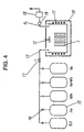
- Fig. 4 is a schematic process diagram describing a hard layer forming means for a metal plate used in the circuit board manufacturing method of the present invention.
- heat treatment furnace 10 is of double structure in which heater 11 is disposed.
- Gas intake pipe 13 and exhaust pipe 14 are connected to an inside of the heat treatment furnace 10 in which is installed a fan 12 for making the internal atmosphere uniform.
- the gas intake pipe 13 is connected via valve 16 and flow meter 17 to a cylinder 15 for supplying various kinds of gas.
- vacuum pump 19 and exhaust gas treatment device 18 are connected to the exhaust pipe.
- Metal plate 1 to be treated to have hard coat layer is disposed in the heat treatment furnace 10 by means of a proper holding jig (not shown).
- a hard coat layer forming method will be briefly described in the following. After a fleon-cleaning of a plate material (1 mm thick) of SUS304 as a metal plate 1, whose surface is polished to 0.1 ⁇ m or less of average surface roughness Ra, the metal plate 1 is put into the heat treatment furnace 10 and is kept in a N 2 gas atmosphere containing 5,000 ppm NF 3 at 280 °C for 15 minutes.
- the temperature is raised to 470 ° C, and the metal plate is kept in an atmosphere of a mixed gas (10 %N 2 + 90 %H 2 ) for 30 minutes, and then is subjected to nitriding treatment for 8 hours in a mixed gas (20 %NH 3 + 80 %RX).
- a mixed gas 10 %N 2 + 90 %H 2
- nitriding treatment for 8 hours in a mixed gas (20 %NH 3 + 80 %RX.
- a carbon atom source in RX it is preferable to use a paraffinic hydrocarbon gas such as methane, ethane, and propane and the like, but it is not limited to such gas, and any type of gas can be used if the gas contains carbon atom.
- nitride layer (hard coat layer) of about 20 ⁇ m in thickness is uniformly formed on a surface of the metal plate 1.
- oxide or the like on the surface of the metal plate 1 is once fluorinated into a fluoride layer and then the fluoride layer is changed to formed a nitride layer, therefore it is possible to assure the uniformity of the nitride layer.
- the treatment temperature is low, there are advantages that the surface smoothness of the metal plate 1 smoothly polished before forming the hard coat layer is not affected and a thermal strain hardly occur in the metal plate 1.
- the treatment temperature is 470 °C, but it is also possible to treat at 400 °C or less depending upon the condition of nitriding to form a more preferable hard coat layer.
- the nitriding method is employed for forming the hard coat layer.
- various methods other than the nitriding method are available for the treatment to obtain the smoothness and hardness of the metal plate surface needed in the present invention.
- the advantages of the present invention may be obtained by selecting a method of treating the metal plate according to the types of circuit board and metal foil or the conditions for the heat press process.
- a surface treating method that is called carbonizing is available as a method in which carbon atom is diffused on the surface of steel material to form a hard coat layer.
- the surface hardness then obtained is 650 to 850 HV, a little lower than the hardness obtained in the nitriding method, but the hard coat layer may be increased as thick as from 0.1 to 2 mm to obtain a metal plate surface substantially very high in rigidity. Accordingly, it is possible to obtain an excellent result by applying the surface treatment in the present invention according to the purpose of the circuit board.
- a method in which both of carbon atom and nitrogen atom are diffused on the surface of the metal plate that is called a carbonitriding method, is preferable for the treatment of a metal plate having an austenite phase.
- the lower the temperature in forming a hard coat layer the better for keeping the surface smoothness of the metal plate, and the metal plate is less strained, and therefore, it is effective to lower the treatment temperature as low as possible.
- a hard coat layer is formed on a metal plate by diffusing an element such as nitrogen atoms or carbon atoms on the surface thereof. It is also possible to employ a method in which a metal or the like completely different materials from the metal plate is formed as a hard coat layer by a vacuum deposition, a sputtering, a deposition or a plating.
- metal nitride is most effective as a hard coat layer in the present invention because of its hardness. And, especially, nitride of titanium or titanium-based metal, that is so-called titanium nitride, is excellent in hardness and adhesion to the stainless steel.
- diamond-like carbon thin film is formed on the surface of a metal plate, it is preferable with respect to the surface hardness, an excellence in sliding ability because of its small friction coefficient, and an advantage such that the metal plate surface is hard to be scratched while the metal plate is conveyed during the process.
- the film in a case the film is not electro-conductive, it is effective to be used in a method where a heat source is obtained by applying an electric current to the copper foils in a heat press process, that is, a method in which the metal plate in the present invention is required to be not electro-conductive.
- the description is made in the case of using the stainless steel plates as the metal plate material, but it is also possible to use a conventional steel material or a non-ferrous metal such as titanium, aluminum and the like as a metal plate.
- the method of manufacturing circuit board in the present invention includes a heat press process in which a laminate with metal foil disposed on both surfaces or one surface of a board material or a board material with metal foil circuit formed thereon is held between metal plates and subjected to a heat press process under at least one of heat and pressing.
- a heat press process it is configured that a hard coat layer is formed on one surface or on both surfaces of the metal plate.
- the metal plate surface is smoothly finished, it is easy to remove contamination such as resins sticking to the metal plate, and it is possible to assure the smoothness for a long period of time because the metal plate surface is very high in hardness.
- the manufacturing process further includes a step of conductive paste compression process or the like, the conductive paste is efficiently compressed since the metal plate has high rigidity, and an improvement of electrical connection reliability between the circuit layers of the circuit board is obtained.
- the present invention is capable of improving the durability of the metal plate by forming a hard coat layer on the metal plate surface used in the circuit board production, and also able to enhance the smoothness of the surface of the circuit board. Accordingly, the present invention is appropriate for the production of the high-quality and highly reliable circuit boards, high density circuit boards in particular.
Landscapes
- Chemical & Material Sciences (AREA)
- Engineering & Computer Science (AREA)
- Mechanical Engineering (AREA)
- Chemical Kinetics & Catalysis (AREA)
- Materials Engineering (AREA)
- Metallurgy (AREA)
- Organic Chemistry (AREA)
- Manufacturing & Machinery (AREA)
- Microelectronics & Electronic Packaging (AREA)
- Laminated Bodies (AREA)
- Production Of Multi-Layered Print Wiring Board (AREA)
- Manufacturing Of Printed Wiring (AREA)
Abstract
Description
Claims (20)
- A method of manufacturing circuit board comprising:holding a laminate between metal plates provided with hard coat layer on at least one surface thereof, said laminate comprising metal foil or resin-coated metal foil disposed on both surfaces or on one surface of a board material or board material with circuit formed thereon; andpressing said laminate by applying at least one of heat and pressure.
- The method of manufacturing circuit board of claim 1, wherein said metal plate is made of one of iron and a material mainly including iron.
- The method of manufacturing circuit board of claim 1, wherein said metal plate is made of a stainless steel.
- The method of manufacturing circuit board of any one of claims 1, 2 and 3, wherein said metal plate is made of a material having a Vickers hardness of 300 HV or more.
- The method of manufacturing circuit board of claim 1, wherein said hard coat layer is formed by implanting or diffusing an element different from main material of the metal plate onto the surface of said metal plate.
- The method of manufacturing circuit board of claim 5, wherein said element is one selected from the group consisting of nitrogen, carbon, and boron.
- The method of manufacturing circuit board of claim 1, wherein said hard coat layer is formed by at least one treatment selected from the group consisting of carbonizing, nitriding, and carbonitriding.
- The method of manufacturing circuit board of claim 5 or 7, wherein the method further comprises forming a metal fluoride layer on said metal plate surface prior to the implanting or the diffusing said element on the metal plate surface.
- The method of manufacturing circuit board of claim 1, wherein said hard coat layer is a formed on the metal plate surface by one of a vacuum deposition, a sputtering, a deposition and a plating.
- The method of manufacturing circuit board of claim 9, wherein said hard coat layer is made of a metal nitride.
- The method of manufacturing circuit board of claim 10, wherein said metal for forming said metal nitride is titanium or a compound mainly containing titanium.
- The method of manufacturing circuit board of claim 9, wherein said hard coat layer is made of a diamond-like carbon.
- The method of manufacturing circuit board of claim 1, wherein said hard layer is 10 µm or more in thickness.
- The method of manufacturing circuit board of claim 1, wherein a surface hardness of said hard coat layer is 500 HV or more in Vickers hardness.
- The method of manufacturing circuit board of claim 1, wherein an average surface roughness Ra of said hard coat layer surface or said metal plate surface is 0.1 µm or less, where the average surface roughness Ra is defined in JIS B0601.
- The method of manufacturing circuit board of claim 1, wherein a maximum surface roughness Rmax of said hard coat layer surface or said metal plate surface is 0.1 µm or less, where the maximum surface roughness Rmax is defined in JIS B0601.
- The method of manufacturing circuit board of claim 1, wherein both surfaces or one surface of said metal foil is roughened, and a 10-point average surface roughness Rz is 5 µm or more, where the 10-point average surface roughness Rz is defined in JIS B0601.
- The method of manufacturing circuit board of claim 1, wherein said metal foil is 20 µm or less in thickness.
- The method of manufacturing circuit board of claim 1, further comprising cleaning of said metal plate after said pressing, wherein in said metal plate cleaning, at least one polishing means is used, and a grain size used for all polishing means or at least one for final polishing means has a grain size No. of #800 or more, or the average diameter of grain is 20 µm or less.
- A method of manufacturing circuit board comprising:holding a laminate between metal plates, said laminate comprising metal foil or resin-coated metal foil disposed on both surfaces or on one surface of a board material or board material with circuit formed thereon;pressing said laminate by applying at least one of heat and pressure; andcleaning of said metal plate after said pressing, wherein in said metal plate cleaning, at least one polishing means is used, and a grain size used for all polishing means or at least one for final polishing means has a grain size No. of #800 or more, or the average diameter of grain is 20 µm or less.
Applications Claiming Priority (3)
| Application Number | Priority Date | Filing Date | Title |
|---|---|---|---|
| JP2000347800A JP3729061B2 (en) | 2000-11-15 | 2000-11-15 | Method for manufacturing circuit-formed substrate |
| JP2000347800 | 2000-11-15 | ||
| PCT/JP2001/009907 WO2002041675A1 (en) | 2000-11-15 | 2001-11-13 | Method for manufacturing circuit board |
Publications (2)
| Publication Number | Publication Date |
|---|---|
| EP1261242A1 true EP1261242A1 (en) | 2002-11-27 |
| EP1261242A4 EP1261242A4 (en) | 2006-11-29 |
Family
ID=18821477
Family Applications (1)
| Application Number | Title | Priority Date | Filing Date |
|---|---|---|---|
| EP01981091A Withdrawn EP1261242A4 (en) | 2000-11-15 | 2001-11-13 | METHOD FOR MANUFACTURING PRINTED CIRCUIT BOARD |
Country Status (5)
| Country | Link |
|---|---|
| US (1) | US20030047269A1 (en) |
| EP (1) | EP1261242A4 (en) |
| JP (1) | JP3729061B2 (en) |
| CN (1) | CN1319426C (en) |
| WO (1) | WO2002041675A1 (en) |
Families Citing this family (3)
| Publication number | Priority date | Publication date | Assignee | Title |
|---|---|---|---|---|
| GB2529346A (en) | 2011-03-31 | 2016-02-17 | Plasyl Ltd | Improvements for electrical circuits |
| KR101687394B1 (en) * | 2013-06-17 | 2016-12-16 | 주식회사 엘지화학 | Photo-curable and thermo-curable resin composition and dry film solder resist |
| CN109551247B (en) * | 2018-12-06 | 2024-05-14 | 广东诚越新材料科技有限公司 | Copper-based resin prepreg production equipment for mobile communication circuit board |
Family Cites Families (14)
| Publication number | Priority date | Publication date | Assignee | Title |
|---|---|---|---|---|
| JPS5222380B2 (en) * | 1973-05-30 | 1977-06-17 | ||
| JPS61289690A (en) * | 1985-06-18 | 1986-12-19 | 川崎製鉄株式会社 | Printed circuit board |
| GB8608717D0 (en) * | 1986-04-10 | 1986-05-14 | Lucas Ind Plc | Metal components |
| US5254181A (en) * | 1989-06-10 | 1993-10-19 | Daidousanso Co., Ltd. | Method of nitriding steel utilizing fluoriding |
| US5244375A (en) * | 1991-12-19 | 1993-09-14 | Formica Technology, Inc. | Plasma ion nitrided stainless steel press plates and applications for same |
| US5403409A (en) * | 1993-03-01 | 1995-04-04 | Daidousanso Co., Ltd. | Nitrided stainless steel products |
| US5536549A (en) * | 1993-08-02 | 1996-07-16 | Tulip Memory Systems, Inc. | Austenitic stainless steel substrate for magnetic-recording media |
| JP2881111B2 (en) * | 1994-06-17 | 1999-04-12 | 大同ほくさん株式会社 | Steel nitriding method |
| JPH09153682A (en) * | 1995-11-29 | 1997-06-10 | Mitsubishi Rayon Co Ltd | Method for manufacturing multilayer printed circuit board |
| US5945214C1 (en) * | 1996-08-28 | 2002-04-23 | Premark Rwp Holdings Inc | Diboride coated pressing surfaces for abrasion resistant laminate and making pressing surfaces |
| DE19651953A1 (en) * | 1996-12-13 | 1998-07-02 | Bayer Bitterfeld Gmbh | Device for pressing flowable solids or semi-solid materials |
| JP3879159B2 (en) * | 1997-01-09 | 2007-02-07 | 松下電器産業株式会社 | Manufacturing method of multilayer printed wiring board |
| JPH1191035A (en) * | 1997-09-24 | 1999-04-06 | Matsushita Electric Works Ltd | Manufacture of laminate board |
| AT409612B (en) * | 1999-01-21 | 2002-09-25 | Boehler Bleche Gmbh | DISK-SHAPED PRESS TOOL AND METHOD FOR THE PRODUCTION THEREOF |
-
2000
- 2000-11-15 JP JP2000347800A patent/JP3729061B2/en not_active Expired - Fee Related
-
2001
- 2001-11-13 CN CNB018036767A patent/CN1319426C/en not_active Expired - Fee Related
- 2001-11-13 WO PCT/JP2001/009907 patent/WO2002041675A1/en not_active Ceased
- 2001-11-13 EP EP01981091A patent/EP1261242A4/en not_active Withdrawn
- 2001-11-13 US US10/181,029 patent/US20030047269A1/en not_active Abandoned
Also Published As
| Publication number | Publication date |
|---|---|
| JP3729061B2 (en) | 2005-12-21 |
| US20030047269A1 (en) | 2003-03-13 |
| WO2002041675A1 (en) | 2002-05-23 |
| CN1319426C (en) | 2007-05-30 |
| EP1261242A4 (en) | 2006-11-29 |
| JP2002151843A (en) | 2002-05-24 |
| CN1395815A (en) | 2003-02-05 |
Similar Documents
| Publication | Publication Date | Title |
|---|---|---|
| KR100506235B1 (en) | Integrated pad and belt for chemical mechanical polishing | |
| US5858517A (en) | Electrodeposited copper foil for printed wiring board and method of manufacturing the same | |
| JP3291482B2 (en) | Flattened electrolytic copper foil, its production method and use | |
| KR101328314B1 (en) | Gravure Printing Engraving Roll and Manufacturing Method thereof | |
| KR101494912B1 (en) | Lapping Carrier and Method | |
| CN1278484A (en) | Coated press-surfacelayer for wear-resisting laminated plate and laminated plate made using same | |
| EP1261242A1 (en) | Method for manufacturing circuit board | |
| EP1060297A2 (en) | Electrolytic copper foil having a modified shiny side | |
| US7716825B2 (en) | Method for manufacturing printed wiring board | |
| JP2002252440A (en) | Intermediate plate for manufacturing circuit-formed substrate and method of manufacturing the same | |
| WO1997047223A1 (en) | Electric liquid heating vessels | |
| JP3132965B2 (en) | Roller surface antifouling treatment method | |
| JP2000218644A (en) | Platelike pressing tool and manufacture thereof | |
| CN101160212A (en) | Surface-treated doctor blades | |
| JP3710741B2 (en) | Cushion material for manufacturing circuit-formed substrate and method | |
| KR20160092359A (en) | Gravure roller and gravure printing apparatus including the same | |
| US20070218587A1 (en) | Soft conductive polymer processing pad and method for fabricating the same | |
| JP5593842B2 (en) | Air slide device | |
| WO2003103934A1 (en) | Industrial elastic belt and method for manufacture thereof | |
| AU2005226311A1 (en) | Press roll for paper machine, method of manufacturing the same, pressing method for wet paper, and surface polishing method for paper machine press roll | |
| JP3434072B2 (en) | Manufacturing method of electrolytic copper foil | |
| KR100535113B1 (en) | A Photosensitive Polymer-based Relief Printing Plate Having Vapor Deposition Layer Thereon and A Method for Preparing the Same | |
| JP2004034679A (en) | Method and apparatus for surface roughening of resin film, and film whose surface is roughened by this method | |
| JPH08125336A (en) | Method of manufacturing thin film multilayer wiring | |
| CN118201214A (en) | Manufacturing process of embedded resistor of printed circuit board |
Legal Events
| Date | Code | Title | Description |
|---|---|---|---|
| PUAI | Public reference made under article 153(3) epc to a published international application that has entered the european phase |
Free format text: ORIGINAL CODE: 0009012 |
|
| 17P | Request for examination filed |
Effective date: 20020715 |
|
| AK | Designated contracting states |
Kind code of ref document: A1 Designated state(s): AT BE CH CY DE DK ES FI FR GB GR IE IT LI LU MC NL PT SE TR |
|
| RBV | Designated contracting states (corrected) |
Designated state(s): AT BE CH DE FR GB LI |
|
| A4 | Supplementary search report drawn up and despatched |
Effective date: 20061027 |
|
| RIC1 | Information provided on ipc code assigned before grant |
Ipc: B32B 15/08 20060101ALI20061023BHEP Ipc: H05K 3/46 20060101ALI20061023BHEP Ipc: B30B 15/06 20060101ALI20061023BHEP Ipc: H05K 3/00 20060101AFI20020527BHEP |
|
| 17Q | First examination report despatched |
Effective date: 20071109 |
|
| STAA | Information on the status of an ep patent application or granted ep patent |
Free format text: STATUS: THE APPLICATION IS DEEMED TO BE WITHDRAWN |
|
| 18D | Application deemed to be withdrawn |
Effective date: 20080320 |