EP1261035A2 - Enhancement- and depletion-mode phemt device and method of forming same - Google Patents
Enhancement- and depletion-mode phemt device and method of forming same Download PDFInfo
- Publication number
- EP1261035A2 EP1261035A2 EP02253498A EP02253498A EP1261035A2 EP 1261035 A2 EP1261035 A2 EP 1261035A2 EP 02253498 A EP02253498 A EP 02253498A EP 02253498 A EP02253498 A EP 02253498A EP 1261035 A2 EP1261035 A2 EP 1261035A2
- Authority
- EP
- European Patent Office
- Prior art keywords
- layer
- enhancement
- recess
- depletion
- ingap
- Prior art date
- Legal status (The legal status is an assumption and is not a legal conclusion. Google has not performed a legal analysis and makes no representation as to the accuracy of the status listed.)
- Withdrawn
Links
Images



Classifications
-
- H—ELECTRICITY
- H10—SEMICONDUCTOR DEVICES; ELECTRIC SOLID-STATE DEVICES NOT OTHERWISE PROVIDED FOR
- H10D—INORGANIC ELECTRIC SEMICONDUCTOR DEVICES
- H10D30/00—Field-effect transistors [FET]
- H10D30/40—FETs having zero-dimensional [0D], one-dimensional [1D] or two-dimensional [2D] charge carrier gas channels
- H10D30/47—FETs having zero-dimensional [0D], one-dimensional [1D] or two-dimensional [2D] charge carrier gas channels having two-dimensional [2D] charge carrier gas channels, e.g. nanoribbon FETs or high electron mobility transistors [HEMT]
-
- H—ELECTRICITY
- H10—SEMICONDUCTOR DEVICES; ELECTRIC SOLID-STATE DEVICES NOT OTHERWISE PROVIDED FOR
- H10D—INORGANIC ELECTRIC SEMICONDUCTOR DEVICES
- H10D84/00—Integrated devices formed in or on semiconductor substrates that comprise only semiconducting layers, e.g. on Si wafers or on GaAs-on-Si wafers
- H10D84/01—Manufacture or treatment
-
- H—ELECTRICITY
- H10—SEMICONDUCTOR DEVICES; ELECTRIC SOLID-STATE DEVICES NOT OTHERWISE PROVIDED FOR
- H10D—INORGANIC ELECTRIC SEMICONDUCTOR DEVICES
- H10D30/00—Field-effect transistors [FET]
- H10D30/40—FETs having zero-dimensional [0D], one-dimensional [1D] or two-dimensional [2D] charge carrier gas channels
- H10D30/47—FETs having zero-dimensional [0D], one-dimensional [1D] or two-dimensional [2D] charge carrier gas channels having two-dimensional [2D] charge carrier gas channels, e.g. nanoribbon FETs or high electron mobility transistors [HEMT]
- H10D30/471—High electron mobility transistors [HEMT] or high hole mobility transistors [HHMT]
- H10D30/473—High electron mobility transistors [HEMT] or high hole mobility transistors [HHMT] having confinement of carriers by multiple heterojunctions, e.g. quantum well HEMT
- H10D30/4732—High electron mobility transistors [HEMT] or high hole mobility transistors [HHMT] having confinement of carriers by multiple heterojunctions, e.g. quantum well HEMT using Group III-V semiconductor material
-
- H—ELECTRICITY
- H10—SEMICONDUCTOR DEVICES; ELECTRIC SOLID-STATE DEVICES NOT OTHERWISE PROVIDED FOR
- H10D—INORGANIC ELECTRIC SEMICONDUCTOR DEVICES
- H10D84/00—Integrated devices formed in or on semiconductor substrates that comprise only semiconducting layers, e.g. on Si wafers or on GaAs-on-Si wafers
- H10D84/01—Manufacture or treatment
- H10D84/0123—Integrating together multiple components covered by H10D12/00 or H10D30/00, e.g. integrating multiple IGBTs
- H10D84/0126—Integrating together multiple components covered by H10D12/00 or H10D30/00, e.g. integrating multiple IGBTs the components including insulated gates, e.g. IGFETs
- H10D84/0158—Integrating together multiple components covered by H10D12/00 or H10D30/00, e.g. integrating multiple IGBTs the components including insulated gates, e.g. IGFETs the components including FinFETs
Definitions
- the present invention generally relates to integrated circuits comprising both enhancement-mode and depletion-mode pseudomorphic high electron mobility transistor (PHEMT) devices and to methods of manufacturing the same.
- PHEMT pseudomorphic high electron mobility transistor
- FETs field effect transistors
- MESFETs metal semiconductor field effect transistors
- HEMTs high electron mobility transistors
- a HEMT is distinguished from a MESFET in that charge is transferred from a charge donor layer to an undoped channel layer in a HEMT.
- HEMTs There are generally two types of HEMTs. One type is referred to simply as a HEMT, whereas the other type is referred to as a pseudomorphic HEMT or PHEMT.
- the difference between the HEMT and the PHEMT is that, in the PHEMT, one or more of the layers incorporated into the device has a lattice constant which differs significantly from the lattice constants of other materials of the device.
- the crystal structure of the material forming the channel layer is strained.
- this lattice mismatch and the attendant strain makes growth of such devices more difficult than the growth of HEMTs, several performance advantages are obtained. For example, the charge density transferred into the channel layer is increased and high electron mobility and high electron saturated velocity are observed. As a result, the devices can develop higher power levels and can operate at higher frequencies with improved noise properties.
- DCFL direct-coupled FET logic
- An enhancement-type transistor is a transistor that blocks the flow of current when no gate-source voltage is applied (also called a normally-off transistor).
- a depletion-type transistor is a transistor that allows current to flow when no gate-source voltage is applied (also called a normally-on transistor).
- the thickness of the active region upon which the gate contact is formed is different for each of these transistors, with this thickness being smaller for the enhancement-type transistor than it is for the depletion-type transistor.
- the present invention is directed to novel PHEMT devices having both an enhancement-mode and a depletion-mode transistor (also referred to herein as “enhancement/depletion PHEMT devices”) and to methods for making the same.
- a depletion/enhancement PHEMT device structure comprises: (a) a semiconductor substrate; (b) a buffer region comprising one or more semiconductor buffer layers over the substrate; (c) a III-V semiconductor channel layer over the buffer region; (d) an electron donor layer over the channel layer; (e) a GaAs or AlGaAs first schottky layer over the electron donor layer; (f) a first InGaP layer over the first schottky layer; (g) a GaAs or AlGaAs second schottky layer over the first InGaP layer; (h) a second InGaP layer over the second schottky layer; (i) a doped GaAs contact layer over the second InGaP layer; (j) an isolation structure extending from an upper surface of the contact layer at least to the buffer region, the isolation structure defining a first active region and a second active region; (k) an isolation structure extending from an upper surface of the contact layer at least
- the semiconductor substrate is a GaAs substrate
- the III-V semiconductor channel layer is an InGaAs channel layer
- the electron donor layer is a plane of silicon atoms.
- the buffer region is preferably one comprising one or more III-V semiconductor layers, more preferably one comprising a GaAs buffer layer and a superlattice buffer comprising alternating layers of GaAs and AlGaAs.
- the first schottky layer is preferably from 50 to 150 Angstroms in thickness, is preferably an Al x Ga 1-x As layer, in which x ranges from 0.35 to 0.75, and is preferably undoped.
- the second schottky layer is preferably from 50 to 150 Angstroms in thickness, is preferably an Al x Ga 1-x As layer in which x ranges from 0.15 to 0.25, and is preferably doped.
- the first and second InGaP layers are preferably In z Ga 1-z P layers in which z ranges from 0.4 to 0.6, and they preferably range from 10 to 50 Angstroms in thickness.
- the isolation structure is preferably an ion implanted structure.
- the depletion/enhancement PHEMT device structure further comprises (a) a doped GaAs or AlGaAs transition layer between the second InGaP layer and the doped GaAs contact layer, in which the transition layer has a lower net doping concentration than the contact layer, (b) an undoped GaAs cap layer between the first schottky layer and the first InGaP layer, in which the cap layer ranges from 15 to 50 Angstroms in thickness, and/or (c) an AlGaAs spacer layer between the channel layer and the electron donor layer.
- the depletion gate recess is greater in aperture within its upper portions than it is within its lower portions, and the enhancement gate recess is greater in aperture within its upper portions than within its lower portions. More preferably, the depletion gate recess is greater in aperture within the doped GaAs contact layer than it is within the second InGaP layer, while the enhancement recess is greater in aperture within the doped GaAs contact layer and the second InGaP layer than it is within the second schottky layer and the first InGaP layer.
- a method of forming a depletion/enhancement PHEMT device structure comprises:
- the enhancement gate recess and the depletion gate recess are preferably etched using wet etching processes.
- the enhancement gate recess is etched by a process that includes the following steps: (a) etching a first active area recess from an upper surface of the contact layer to an upper surface of the second InGaP layer in a first enhancement recess etching step; (b) further etching the first active area recess through the second InGaP layer in a second enhancement recess etching step; (c) further etching the first active area recess to an upper surface of the first InGaP layer in a third enhancement recess etching step; and (d) further etching the first active area recess through the first InGaP layer in a fourth enhancement recess etching step to complete the enhancement gate recess.
- the depletion gate recess is etched by a process that preferably includes the following steps: (a) etching a second active area recess from an upper surface of the contact layer to an upper surface of the second InGaP layer in a first depletion recess etching step; and (b) further etching the second active area recess through the second InGaP layer in a second depletion recess etching step to complete the depletion gate recess.
- the first enhancement recess etching step, the third enhancement recess etching step and the first depletion recess etching step are preferably conducted using an aqueous etching solution comprising H 2 SO 4 and H 2 O 2
- the second enhancement recess etching step, the fourth enhancement recess etching step, and the second depletion etching step are preferably conducted using an aqueous etching solution comprising HCl.
- the first and second enhancement recess etching steps are preferably conducted such that an upper first active area recess having a first aperture is formed within the doped GaAs contact layer and within the second InGaP layer; and the third and fourth enhancement etching steps are preferably conducted such that a lower first active area recess having a second aperture narrower than the first aperture is formed within the second schottky layer and within the first InGaP layer.
- the third enhancement recess etching step is preferably performed concurrently with the first depletion recess etching step
- the fourth enhancement recess etching step is preferably performed concurrently with the second depletion recess etching step
- the enhancement gate contact is preferably deposited concurrently with the depletion gate contact.
- the multi-layer structure further comprises a doped GaAs or AlGaAs transition layer between the second InGaP layer and the doped GaAs contact layer, with the transition layer having a lower net doping concentration than the contact layer.
- the enhancement gate recess is etched within this group of embodiments by a process comprising the following: (a) etching a first active area recess from an upper surface of the contact layer to an upper surface of the second InGaP layer in a first enhancement recess etching step; (b) further etching the first active area recess through the second InGaP layer in a second enhancement recess etching step; (c) further etching the first active area recess to an upper surface of the first InGaP layer in a third enhancement recess etching step; and (d) further etching the first active area recess through the first InGaP layer in a fourth enhancement recess etching step to complete the enhancement gate recess.
- the depletion gate recess is etched within this group of embodiments by a process comprising the following: (a) etching a second active area recess from an upper surface of the contact layer to an upper surface of the transition layer in a first depletion recess etching step; (b) further etching the second active area recess to an upper surface of the second InGaP layer in a second depletion recess etching step; and (c) further etching the second active area recess through the second InGaP layer in a third depletion recess etching step to complete the depletion gate recess.
- the first and second enhancement recess etching steps are preferably conducted such that an upper first active area recess having a first aperture is formed within the doped GaAs contact layer, within the transition layer, and within the second InGaP layer
- the third and fourth enhancement recess etching steps are preferably conducted such that a lower first active area recess having a second aperture narrower than the first aperture is formed within the second schottky layer and within the first InGaP layer
- the first depletion recess etching step is preferably conducted such that an upper second active area recess having a third aperture is formed within the doped GaAs contact layer
- the second and third depletion recess etching steps are preferably conducted such that a lower second active area recess having a fourth aperture that is narrower than the third aperture is formed within the transition layer and within the second InGaP layer.
- the third enhancement recess etching step is preferably performed concurrently with the second depletion recess etching step
- the fourth enhancement recess etching step is preferably performed concurrently with the third depletion recess etching step
- the enhancement gate contact is preferably deposited concurrently with the depletion gate contact.
- each of the first enhancement step, the third enhancement recess etching step and the second depletion recess etching step is preferably conducted using an aqueous etching solution comprising H 2 SO 4 and H 2 O 2
- each of the second enhancement recess etching step, the fourth enhancement recess etching step, and the third depletion step is preferably conducted using an aqueous etching solution comprising HCl.
- One advantage of the present invention is that a PHEMT device containing both enhancement-mode and depletion-mode transistors can be achieved (1) with good control of the thickness of the active region adjacent the gate metal and (2) without using etch-stop materials that increase transistor source resistance.
- another advantage of the present invention is that a PHEMT device containing both enhancement-mode and depletion-mode transistors can be achieved using wet etching techniques that: (1) involve conventional and easily controlled etching chemistry, (2) provide high selectivity, and (3) enable large volume batch mode etch operations, reducing considerably the capital equipment, labor content and cycle time associated with the device.
- Another advantage of the present invention is that a PHEMT device containing both enhancement-mode and depletion-mode transistors can be achieved using relatively few process steps.
- Yet another advantage of the present invention is that a PHEMT device containing both enhancement-mode and depletion-mode transistors can be achieved without resorting to techniques, such as reactive ion etching techniques, that prevent implementation of highly efficient batch-mode processing and can result in crystal damage and degrade transistor performance.
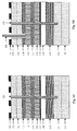
- Figs. 1A-1E are schematic cross-sectional views sequentially illustrating the formation of a PHEMT device containing both enhancement-mode and depletion-mode transistors, according to an embodiment of the invention.
- Figs. 2A-2B are schematic cross-sectional views sequentially illustrating the formation of a PHEMT device containing both enhancement-mode and depletion-mode transistors, according to another embodiment of the invention.
- Figs. 3A-3C are schematic cross-sectional views sequentially illustrating the formation of manufacturing a PHEMT device containing both enhancement-mode and depletion-mode transistors, according to yet another embodiment of the invention.
- a first PHEMT device containing both enhancement-mode and depletion-mode transistors and a method of making the same will now be described in connection with Figs 1A-1E.
- Fig. 1A illustrates a multi-layer structure, the bottom layer of which is a semiconductor substrate 102.
- the semiconductor substrate 102 is preferably a III-V semiconductor substrate and more preferably an undoped GaAs substrate.
- the specific buffer region used in this embodiment includes a buffer layer 104 of undoped GaAs (which can be, e.g., 1000 to 10000 ⁇ thick) as well as a superlattice buffer 106, which is preferably composed of alternating layers of GaAs (which can be, for example, 15-50 ⁇ thick) and Al x Ga 1-x As (which can be, for example, 15 to 300 ⁇ thick), where x typically ranges from 0.1 to 0.4.
- the superlattice buffer 106 generally contains 5 to 30 periods (10 to 60 alternating layers) and preferably terminates with a layer of Al x Ga 1-x As.
- buffer layer 104 and superlattice buffer 106 are preferably grown over the substrate by techniques commonly used in the art, such as molecular beam epitaxy (MBE) and/or metal-organic chemical vapor deposition (MOCVD).
- MBE molecular beam epitaxy
- MOCVD metal-organic chemical vapor deposition
- III-V semiconductor channel layer 108 which is preferably an InGaAs layer and, more preferably, an undoped In y Ga 1-y As channel layer, where y preferably ranges from of 0.1 to 0.3 and where the thickness ranges from 60 to 180 ⁇ .
- a spacer layer (not shown) is provided on the channel layer 108.
- the spacer layer can be, for example, a layer of undoped AlGaAs, more preferably a 20 to 60 ⁇ layer of Al x Ga 1-x As, where x ranges from 0.15 to 0.25.
- a charge donor layer 110 is then provided. Any appropriate charge donor layer 110 known in the art for this purpose can be used. In the specific example of Fig. 1A, this layer is a plane of silicon atoms.
- a thin cap layer (not shown) is provided upon the first schottky layer 112 for oxidation protection.
- the cap layer can be a thin (e.g., 15 to 50 ⁇ ) undoped GaAs cap layer.
- a first InGaP etch-stop layer 114 is then deposited on the structure.
- the etch-stop layer 114 is an In z Ga 1-z P layer, where z preferably ranges from 0.4 to 0.6 and where the layer thickness preferably ranges from 10 to 50 ⁇ .
- a GaAs or AlGaAs second schottky layer 116 is then provided, which can be doped or undoped.
- the second schottky layer 116 is an n-doped Al x Ga 1-x As layer of 50 to 150 ⁇ in thickness, where x preferably ranges from 0.15 to 0.25, and where the net doping concentration preferably ranges from 10 16 to 10 18 cm -3 .
- a second InGaP etch-stop layer 118 is deposited over the second schottky layer 116.
- the second etch-stop layer 118 is preferably an In z Ga 1-z P layer, where z ranges from 0.4 to 0.6 and where the layer thickness preferably ranges from 10 to 50 ⁇ .
- the top layer in Fig. 1A is a doped GaAs contact layer 122.
- the doped GaAs contact layer 122 is an n+ doped GaAs contact layer having a preferred thickness of 200-1000 ⁇ and a preferred net doping concentration of 10 18 to 10 19 cm -3 .
- a transition layer 120 is provided between the second InGaP etch-stop layer 118 and the n+ doped GaAs contact layer 122.
- the transition layer 120 is preferably an n-GaAs transition layer having a thickness of 200-500 ⁇ and a net doping concentration of 1x10 17 to 1x10 18 cm -3 .
- Fig. 1A The resulting multi-layer structure is illustrated in Fig. 1A.
- ohmic contacts 124 (four contacts are shown, one of which is labeled) are formed on contact layer 122, preferably using photolithographic and metal deposition techniques commonly used in the manufacture of GaAs monolithic microwave integrated circuits (MMICs).
- MMICs monolithic microwave integrated circuits
- the resulting structure is shown in Fig. 1B.
- the four ohmic contacts 124 illustrated are ultimately used as the source and drain contacts for the enhancement and depletion PHEMTs.
- Preferred metal deposition techniques are evaporation techniques.
- AuGe is a preferred material for the ohmic contacts 124.
- an isolation structure 126 is formed.
- the isolation structure 126 preferably extends from an upper surface of the multi-layer structure to the buffer region and, more preferably, to the buffer layer 104.
- the isolation structure 126 can be formed, for example, using a photolithographic process to define the desired areas followed by ion implantation as is well known in the art. This step defines two active regions: one to the left of the isolation structure 126 (which, in this set of Figures, corresponds ultimately to the depletion mode PHEMT) and one to the right of the isolation structure 126 (which corresponds to the enhancement mode PHEMT).
- An appropriate photolithographic process is then preferably employed to define a photoresist pattern, which includes an opening corresponding to the gate of the depletion-mode PHEMT.
- This photolithographic process is followed by an appropriate etching sequence to form the depletion-mode gate recess.
- a first selective etching step can be performed using, for example, an H 2 SO 4 :H 2 O 2 :H 2 O solution, which etches through the contact layer 122 and the transition layer 120, terminating at the second InGaP etch-stop layer 118.
- the second InGaP etch-stop layer 118 is then etched by a second selective etching step that uses, for example, a solution of HCl:H 2 O.
- This etching step extends the gate recess through the second InGaP etch-stop layer 118.
- Depletion-mode gate metalization 128 is then deposited over the second schottky layer 116 through the opening defined in the photoresist pattern, forming the schottky contact that is used as the gate electrode of the depletion-mode PHEMT.
- Preferred metal deposition techniques are evaporation techniques.
- Preferred gate metalization includes Ti/Pt/Au. The photoresist pattern is removed, resulting in the structure of Fig. 1D.
- An additional photolithographic process is then employed to define a photoresist pattern that includes an opening for the gate of the enhancement-mode PHEMT.
- This photolithographic step is followed by an appropriate etching sequence.
- a selective gate recess etch can be performed using a H 2 SO 4 :H 2 O 2 :H 2 O solution, which terminates at the second InGaP etch-stop layer 118.
- the second InGaP etch-stop layer 118 is then etched using, for example, a solution of HCl:H 2 O.
- the second schottky layer 116 is then etched using, for example, an H 2 SO 4 :H 2 O 2 :H 2 O solution, which etching step terminates at the first InGaP etch-stop layer 114.
- the first InGaP etch-stop layer 114 is then removed using a solution of HCl:H 2 O.
- Enhancement-mode gate metalization 130 is then deposited over the first schottky layer 112 through the opening defined in the photoresist pattern, forming the schottky contact used as the gate electrode of the enhancement-mode PHEMT.
- the photoresist is removed, resulting in the depletion-enhancement PHEMT structure illustrated in Fig. 1E.
- the enhancement-mode PHEMT is provided with a double-recess structure (consisting of an upper recess portion and a lower recess portion).
- This double-recessed design typically has superior breakdown voltages relative to a single-recess design, such as that illustrated in Fig. 1E.
- a multi-layer structure having ohmic contacts 124 and isolation structure 126 is formed, as described above in connection with Figs. 1A-1C.
- an appropriate photolithographic process is employed to define a photoresist pattern that includes an opening corresponding to an upper portion of the gate recess for the enhancement-mode PHEMT.
- This photolithographic step is followed by an appropriate etching step.
- a selective gate recess etch can be performed using a H 2 SO 4 :H 2 O 2 :H 2 O solution, which terminates at the second InGaP etch-stop layer 118.
- the second InGaP etch-stop layer 118 is then removed using, for example, a solution of HCl:H 2 O.
- the resulting structure is illustrated in Fig. 2A
- a further appropriate photolithographic process is then employed to create a photoresist pattern that includes openings for both the lower portion of the gate recess of the enhancement-mode PHEMT and the entire gate recess for the depletion-mode PHEMT.
- the photoresist openings corresponding to the enhancement-mode PHEMT are narrower in this step than in the prior step, creating a double-recess enhancement-mode PHEMT after etching.
- a selective etching step is then performed using, for example, an H 2 SO 4 :H 2 O 2 :H 2 O solution.
- Etching is terminated at the first InGaP etch-stop layer 114 in the region of the enhancement mode gate and at the second InGaP etch-stop layer 118 in the region of the depletion mode gate (this is made possible by formation of the initial enhancement-mode recess illustrated in Fig. 2A). Then, using a solution of HCl:H 2 O, for example, the first InGaP etch-stop layer 114 is removed in the area of the enhancement-mode gate, and the second InGaP etch-stop layer 118 is removed in the area of the depletion-mode gate.
- Enhancement-mode gate metalization 130 and depletion-mode gate metalization 128 are then deposited through the openings defined in the photoresist pattern, forming the schottky contacts used as the gate electrodes of the enhancement- and depletion-mode PHEMTs.
- the photoresist pattern is removed, producing the structure illustrated in Fig. 2B.
- the stepped (or double) recess for the enhancement-mode gate metalization 130 can be clearly seen in this figure.
- the depletion-mode gate metalization 128 of Fig. 2B does not contain a stepped recess.
- a method of forming an enhancement/depletion PHEMT device in which both the enhancement-mode gate metalization 130 and the depletion-mode gate metalization 128 have stepped recesses will now be described in connection with Figs 3A-3C.
- a multi-layer structure which includes ohmic contacts 124 and isolation structure 126, is formed as described above in connection with Figs. 1A-1C.
- an appropriate photolithographic process is employed to define a photoresist pattern that includes an opening corresponding to an upper gate recess for the depletion-mode PHEMT.
- a non-selective gate recess etching step using any one of a number of appropriate GaAs etch solutions known in the art, to etch the structure down to the transition layer 120.
- the photoresist is removed, resulting in the structure of Fig. 3A.
- An additional photoresist pattern is defined, which includes an opening corresponding an upper gate recess for the enhancement-mode PHEMT.
- This photolithographic step is followed by an appropriate etching step.
- a selective gate recess etch can be performed, for example, using an H 2 SO 4 :H 2 O 2 :H 2 O solution, which terminates at the second InGaP etch-stop layer 118.
- the second InGaP etch-stop layer 118 is then removed using, for example, a solution of HCl:H 2 O.
- the photoresist is then removed.
- the resulting structure is illustrated in Fig. 3B.
- a further photoresist pattern is defined, which includes openings for both the lower gate recess of the enhancement-mode PHEMT and the lower gate recess of the depletion-mode PHEMT.
- the openings for the lower gate recesses of the enhancement- and depletion-mode PHEMTs are narrower than the corresponding openings for the upper gate recesses, creating double recesses after etch.
- a selective gate recess etch is performed, for example, using a H 2 SO 4 :H 2 O 2 :H 2 O solution that stops (a) at the first InGaP etch-stop layer 114 in the region of the enhancement mode gate and (b) at the second InGaP etch-stop layer 118 in the region of the depletion mode gate.
- Enhancement-mode gate metalization 130 and depletion-mode gate metalization 128 are then deposited through the openings defined in the photoresist pattern to form the schottky contacts that are used as the gate electrodes of the enhancement- and depletion-mode PHEMTs.
- the photoresist pattern is then removed, resulting in the structure illustrated in Fig. 3C. Due to the double recessed structure, the design shown has superior breakdown voltage in connection with both the enhancement-mode PHEMT and depletion-mode PHEMT.
Landscapes
- Junction Field-Effect Transistors (AREA)
- Electrodes Of Semiconductors (AREA)
- Weting (AREA)
Abstract
Description
Claims (26)
- A depletion/enhancement PHEMT device structure comprising:a semiconductor substrate (102);a buffer region comprising one or more semiconductor buffer layers (104,106) over said substrate;a III-V semiconductor channel layer (108) over said buffer region;an electron donor layer (110) over said channel layer;a GaAs or AlGaAs first schottky layer (112) over said electron donor layer;a first InGaP layer (114) over said first schottky layer;a GaAs or AlGaAs second schottky layer (116) over said first InGaP layer;a second InGaP layer (118) over said second schottky layer;a doped GaAs contact layer (122) over said second InGaP layer;an isolation structure (126) extending from an upper surface of said contact layer (122) at least to said buffer region (104,106), said isolation structure defining a first active region and a second active region;an enhancement ohmic source contact (124)and an enhancement ohmic drain contact (124) disposed on said doped GaAs contact layer (122) within said first active region;an enhancement gate recess extending from an upper surface of said contact layer (122) and through said first InGaP layer (114) within said first active region;an enhancement gate contact (130) disposed over said first schottky layer within said enhancement gate recess;a depletion ohmic source contact (124) and a depletion ohmic drain contact (124) disposed on said doped GaAs contact layer within said second active region;a depletion gate recess extending from an upper surface of said contact layer and through said second InGaP layer (118) within said second active region; anda depletion gate contact (128) disposed over said second schottky layer within said depletion gate recess.
- The depletion/enhancement PHEMT device structure of claim 1, wherein said semiconductor substrate (102) is a GaAs substrate.
- The depletion/enhancement PHEMT device structure of claim 1 or 2, wherein said one or more buffer layers (104),106) consist of one or more III-V semiconductor layers.
- The depletion/enhancement PHEMT device structure of claim 3, wherein said one or more buffer layers comprise a GaAs buffer layer (104) and a superlattice buffer (106) comprising alternating layers of GaAs and AlGaAs.
- The depletion/enhancement PHEMT device structure of any preceding claim, wherein said III-V semiconductor channel layer (108) is an InGaAs channel layer.
- The depletion/enhancement PHEMT device structure of any preceding claim, wherein said electron donor layer (110) is a plane of silicon atoms.
- The depletion/enhancement PHEMT device structure of any preceding claim, wherein said first schottky layer (112) is an AlxGa1-xAs layer in which x ranges from 0.35 to 0.75, wherein said first schottky layer (116) is from 50 to 150 Angstroms in thickness, wherein said second schottky layer is an AlxGa1-xAs layer in which x ranges from 0.15 to 0.25, and wherein said second schottky layer is from 50 to 150 Angstroms in thickness.
- The depletion/enhancement PHEMT device structure of claim 7, wherein said first schottky layer (112) is undoped and said second schottky layer (116) is doped.
- The depletion/enhancement PHEMT device structure of any preceding claim, wherein said first and second InGaP layers (114,118) are InzGa1-zP layers in which z ranges from 0.4 to 0.6, and wherein said first and second InGaP layers are from 10 to 50 Angstroms in thickness.
- The depletion/enhancement PHEMT device structure of any preceding claim, wherein said isolation structure (126) is an ion implanted structure.
- The depletion/enhancement PHEMT device structure of any preceding claim, including a doped GaAs or AlGaAs transition layer (120) between said second InGaP layer (118) and said doped GaAs contact layer (122), said transition layer having a lower net doping concentration than said contact layer.
- The depletion/enhancement PHEMT device structure of any preceding claim, including an undoped GaAs cap layer between said first schottky layer (112) and said first InGaP layer (114), said cap layer (122)ranging from 15 to 50 Angstroms in thickness.
- The depletion/enhancement PHEMT device structure of any preceding claim, including an AlGaAs spacer layer between said channel layer (108) and said electron donor layer (110).
- The depletion/enhancement PHEMT device structure of any preceding claim, wherein said depletion gate recess is greater in aperture within upper portions than within lower portions, and wherein said enhancement gate recess is greater in aperture within upper portions than within lower portions.
- The depletion/enhancement PHEMT device structure of any preceding claim 1 to 13,
wherein said depletion gate recess is greater in aperture within said doped GaAs contact layer than within said second InGaP layer, and
wherein said enhancement recess is greater in aperture within said doped GaAs contact layer and said second InGaP layer than within said second schottky layer and said first InGaP layer. - A method of forming a depletion/enhancement PHEMT device structure comprising:providing a multi-layer structure comprising: (a) a semiconductor substrate (102); (b) a buffer region (104,106) over said substrate, said buffer region comprising one or more semiconductor buffer layers; (c) a III-V semiconductor channel layer (108) over said buffer region; (d) an electron donor layer (110) over said channel layer; (f) a GaAs or AlGaAs first schottky layer (112) over said electron donor layer; (g) a first InGaP layer over said first schottky layer; (h) a GaAs or AlGaAs second schottky layer (116) over said first InGaP layer; (i) a second InGaP layer (118) over said second schottky layer; (j) a doped GaAs contact layer (122) over said second InGaP layer; (k) ohmic contacts (134) disposed on said doped GaAs contact layer; and (l) an isolation structure (126) extending from an upper surface of said contact layer at least to said buffer region (104,106), said isolation structure defining a first active region and a second active region;etching within said first active region an enhancement gate recess that extends from an upper surface of said contact layer (122) through said first InGaP layer (114);depositing an enhancement gate contact (130) over said first schottky layer within said enhancement gate recess;etching within said second active region a depletion gate recess that extends from an upper surface of said contact layer through said second InGaP layer (118); anddepositing a depletion gate contact (128) over said second schottky layer within said depletion gate recess.
- The method of claim 16,
wherein said enhancement gate recess is etched by a process comprising: (a) etching a first active area recess from an upper surface of said contact layer (120) to an upper surface of said second InGaP layer (118) in a first enhancement recess etching step; (b) further etching said first active area recess through said second InGaP layer in a second enhancement recess etching step; (c) further etching said first active area recess to an upper surface of said first InGaP layer (114) in a third enhancement recess etching step; and (d) further etching said first active area recess through said first InGaP layer in a fourth enhancement recess etching step to complete said enhancement gate recess, and
wherein said depletion gate recess is etched by a process comprising: (a) etching a second active area recess from an upper surface of said contact layer (122) to an upper surface of said second InGaP layer (118) in a first depletion recess etching step; and (b) further etching said second active area recess through said second InGaP layer in a second depletion recess etching step to complete said depletion gate recess. - The method of claim 16 or 17, wherein said enhancement gate recess and said depletion gate recess are etched using wet etching processes.
- The method of claim 17 or 18,
wherein each of said first enhancement recess etching step, said third enhancement recess etching step and said first depletion recess etching step is conducted using an aqueous etching solution comprising H2SO4 and H2O2, and
wherein each of said second enhancement recess etching step, said fourth enhancement recess etching step, and said second depletion etching step is conducted using an aqueous etching solution comprising HCl. - The method of claim 17, 18 or 19
wherein said first and second enhancement recess etching steps are conducted such that an upper first active area recess having a first aperture is formed within said doped GaAs contact layer and within said second InGaP layer,
wherein said third and fourth enhancement etching steps are conducted such that a lower first active area recess having a second aperture is formed within said second schottky layer and within said first InGaP layer, and
wherein said first aperture is wider than said second aperture. - The method of claim 17, 18, 19 or 20, wherein said third enhancement recess etching step is performed concurrently with said first depletion recess etching step, wherein said fourth enhancement recess etching step is performed concurrently with said second depletion recess etching step, and wherein said enhancement gate contact is deposited concurrently with said depletion gate contact.
- The method of any preceding claim 17 to 21, wherein no two of said first depletion recess etching step, said second depletion recess etching step, said first enhancement recess etching step, said second enhancement recess etching step, said third enhancement recess etching step, and said fourth enhancement recess etching step are performed concurrently.
- The method of claim 16,
wherein said multi-layer structure includes a doped GaAs or AlGaAs transition layer (120) between said second InGaP layer (118) and said doped GaAs contact layer (122), said transition layer having a lower net doping concentration than said contact layer,
wherein said enhancement gate recess is etched by a process comprising: (a) etching a first active area recess from an upper surface of said contact layer to an upper surface of said second InGaP layer in a first enhancement recess etching step; (b) further etching said first active area recess through said second InGaP layer in a second enhancement recess etching step; (c) further etching said first active area recess to an upper surface of said first InGaP layer in a third enhancement recess etching step; and (d) further etching said first active area recess through said first InGaP layer in a fourth enhancement recess etching step to complete said enhancement gate recess, and
wherein said depletion gate recess is etched by a process comprising: (a) etching a second active area recess from an upper surface of said contact layer to an upper surface of said transition layer in a first depletion recess etching step; (b) further etching said second active area recess to an upper surface of said second InGaP layer in a second depletion recess etching step; and (c) further etching said second active area recess through said second InGaP layer in a third depletion recess etching step to complete said depletion gate recess. - The method of claim 23,
wherein said first and second enhancement recess etching steps are conducted such that an upper first active area recess having a first aperture is formed within said doped GaAs contact layer, within said transition layer, and within said second InGaP layer,
wherein said third and fourth enhancement recess etching steps are conducted such that a lower first active area recess having a second aperture is formed within said second schottky layer and within said first InGaP layer,
wherein said first aperture is wider than said second aperture,
wherein said first depletion recess etching step is conducted such that an upper second active area recess having a third aperture is formed within said doped GaAs contact layer,
wherein said second and third depletion recess etching steps are conducted such that a lower second active area recess having a fourth aperture is formed within said transition layer and within said second InGaP layer, and
wherein said third aperture is wider than said fourth aperture. - The method of claim 23 or 24, wherein said third enhancement recess etching step is performed concurrently with said second depletion recess etching step, wherein said fourth enhancement recess etching step is performed concurrently with said third depletion recess etching step, and wherein said enhancement gate contact is deposited concurrently with said depletion gate contact.
- The method of claim 23, 24 or 25,
wherein each of said first enhancement step, said third enhancement recess etching step and said second depletion recess etching step is conducted using an aqueous etching solution comprising H2SO4 and H2O2, and
wherein each of said second enhancement recess etching step, said fourth enhancement recess etching step, and said third depletion step is conducted using an aqueous etching solution comprising HCl.
Applications Claiming Priority (2)
| Application Number | Priority Date | Filing Date | Title |
|---|---|---|---|
| US09/861,037 US6703638B2 (en) | 2001-05-21 | 2001-05-21 | Enhancement and depletion-mode phemt device having two ingap etch-stop layers |
| US861037 | 2001-05-21 |
Publications (2)
| Publication Number | Publication Date |
|---|---|
| EP1261035A2 true EP1261035A2 (en) | 2002-11-27 |
| EP1261035A3 EP1261035A3 (en) | 2005-02-09 |
Family
ID=25334692
Family Applications (1)
| Application Number | Title | Priority Date | Filing Date |
|---|---|---|---|
| EP02253498A Withdrawn EP1261035A3 (en) | 2001-05-21 | 2002-05-17 | Enhancement- and depletion-mode phemt device and method of forming same |
Country Status (4)
| Country | Link |
|---|---|
| US (1) | US6703638B2 (en) |
| EP (1) | EP1261035A3 (en) |
| JP (2) | JP2003023016A (en) |
| KR (1) | KR100939037B1 (en) |
Cited By (7)
| Publication number | Priority date | Publication date | Assignee | Title |
|---|---|---|---|---|
| WO2005119778A2 (en) | 2004-05-26 | 2005-12-15 | Raytheon Company | Field effect transistor |
| WO2006083587A3 (en) * | 2005-02-04 | 2006-10-12 | Raytheon Co | Monolithic integrated circuit having enhanced breakdown voltage |
| US7498223B2 (en) | 2005-04-01 | 2009-03-03 | Raytheon Company | Semiconductor devices having improved field plates |
| WO2009040509A1 (en) * | 2007-09-25 | 2009-04-02 | Filtronic Compound Semiconductors Limited | A multilayer semiconductor structure, a bifet includin such a structure, and a multilayer semiconductor substrate |
| US7626218B2 (en) | 2005-02-04 | 2009-12-01 | Raytheon Company | Monolithic integrated circuit having enhancement mode/depletion mode field effect transistors and RF/RF/microwave/milli-meter wave milli-meter wave field effect transistors |
| CN103337460A (en) * | 2013-06-09 | 2013-10-02 | 中国电子科技集团公司第五十五研究所 | Preparation method of E/D integrated GaN HEMT device |
| EP2434538A4 (en) * | 2009-05-19 | 2014-04-30 | Murata Manufacturing Co | SEMICONDUCTOR SWITCHING DEVICE AND METHOD FOR MANUFACTURING SEMICONDUCTOR SWITCHING DEVICE |
Families Citing this family (30)
| Publication number | Priority date | Publication date | Assignee | Title |
|---|---|---|---|---|
| US6787826B1 (en) | 2003-03-14 | 2004-09-07 | Triquint Semiconductor, Inc. | Heterostructure field effect transistor |
| US7449728B2 (en) * | 2003-11-24 | 2008-11-11 | Tri Quint Semiconductor, Inc. | Monolithic integrated enhancement mode and depletion mode field effect transistors and method of making the same |
| US7488992B2 (en) * | 2003-12-04 | 2009-02-10 | Lockheed Martin Corporation | Electronic device comprising enhancement mode pHEMT devices, depletion mode pHEMT devices, and power pHEMT devices on a single substrate and method of creation |
| JP4284254B2 (en) | 2004-09-07 | 2009-06-24 | 富士通株式会社 | Field effect semiconductor device |
| TW200627627A (en) * | 2004-09-24 | 2006-08-01 | Koninkl Philips Electronics Nv | Enhancement-depletion field effect transistor structure and method of manufacture |
| JP2008527687A (en) * | 2004-12-30 | 2008-07-24 | オーミック ソシエテ パール アクション サンプリフィエ | Enhancement-depletion semiconductor structure and manufacturing method thereof |
| US7321132B2 (en) * | 2005-03-15 | 2008-01-22 | Lockheed Martin Corporation | Multi-layer structure for use in the fabrication of integrated circuit devices and methods for fabrication of same |
| US7253455B2 (en) * | 2005-04-05 | 2007-08-07 | Freescale Semiconductor, Inc. | pHEMT with barrier optimized for low temperature operation |
| JP2007227884A (en) * | 2006-01-30 | 2007-09-06 | Matsushita Electric Ind Co Ltd | Field effect transistor |
| US7808016B2 (en) * | 2006-09-14 | 2010-10-05 | Teledyne Licensing, Llc | Heterogeneous integration of low noise amplifiers with power amplifiers or switches |
| JP2010506397A (en) * | 2006-10-04 | 2010-02-25 | セレックス システミ インテグラティ エッセ. ピ. ア. | Single voltage supply type pseudomorphic high electron mobility transistor (PHEMT) power device and manufacturing method thereof |
| JP2008263146A (en) * | 2007-04-13 | 2008-10-30 | Matsushita Electric Ind Co Ltd | Semiconductor device and manufacturing method thereof |
| US20090073065A1 (en) * | 2007-09-14 | 2009-03-19 | M/A-Com, Inc. | Tunable Dielectric Resonator Circuit |
| JP2009224605A (en) * | 2008-03-17 | 2009-10-01 | Panasonic Corp | Semiconductor device and its manufacturing method |
| JP2010135590A (en) * | 2008-12-05 | 2010-06-17 | Renesas Electronics Corp | Field-effect transistor |
| JP5749918B2 (en) * | 2010-11-18 | 2015-07-15 | ルネサスエレクトロニクス株式会社 | Semiconductor device and manufacturing method of semiconductor device |
| ITTO20120675A1 (en) | 2011-08-01 | 2013-02-02 | Selex Sistemi Integrati Spa | PHEMT DEVICE FOR ENRICHMENT / EMPTYING AND ITS MANUFACTURING METHOD |
| US9129827B2 (en) * | 2012-04-13 | 2015-09-08 | Intel Corporation | Conversion of strain-inducing buffer to electrical insulator |
| TWI615977B (en) * | 2013-07-30 | 2018-02-21 | 高效電源轉換公司 | Integrated circuit with matching threshold voltage and manufacturing method thereof |
| WO2015026371A1 (en) | 2013-08-23 | 2015-02-26 | Intel Corporation | High resistance layer for iii-v channel deposited on group iv substrates for mos transistors |
| US9502535B2 (en) * | 2015-04-10 | 2016-11-22 | Cambridge Electronics, Inc. | Semiconductor structure and etch technique for monolithic integration of III-N transistors |
| US20170076986A1 (en) * | 2015-07-15 | 2017-03-16 | The Regents Of The University Of Michigan | Non-destructive epitaxial lift-off of large area iii-v thin-film grown by metal organic chemical vapor deposition and substrate reuse |
| US10720428B2 (en) * | 2015-11-10 | 2020-07-21 | Qorvo Us, Inc. | High bandgap Schottky contact layer device |
| EP3182460A1 (en) * | 2015-12-18 | 2017-06-21 | IMEC vzw | Method of fabricating an enhancement mode group iii-nitride hemt device and a group iii-nitride structure fabricated thereof |
| WO2018182704A1 (en) * | 2017-03-31 | 2018-10-04 | Intel Corporation | Enhancement/depletion device pairs and methods of producing the same |
| US11658236B2 (en) * | 2019-05-07 | 2023-05-23 | Cambridge Gan Devices Limited | III-V semiconductor device with integrated power transistor and start-up circuit |
| CN112635540B (en) * | 2019-10-08 | 2022-09-09 | 无锡华润上华科技有限公司 | LDMOS device and preparation method thereof |
| US11081485B2 (en) * | 2019-10-23 | 2021-08-03 | Win Semiconductors Corp. | Monolithic integrated circuit device having gate-sinking pHEMTs |
| CN116364548A (en) * | 2021-12-28 | 2023-06-30 | 华润微电子(重庆)有限公司 | HEMT device and its preparation method |
| CN118398494B (en) * | 2024-06-28 | 2024-09-27 | 合肥欧益睿芯科技有限公司 | E/D integrated GaAs HEMT device, manufacturing method, circuit and electronic equipment thereof |
Family Cites Families (26)
| Publication number | Priority date | Publication date | Assignee | Title |
|---|---|---|---|---|
| DE3480631D1 (en) | 1983-06-24 | 1990-01-04 | Nec Corp | SEMICONDUCTOR STRUCTURE WITH HIGH GRID DENSITY. |
| DE3476841D1 (en) | 1983-11-29 | 1989-03-30 | Fujitsu Ltd | Compound semiconductor device and method of producing it |
| US5091759A (en) | 1989-10-30 | 1992-02-25 | Texas Instruments Incorporated | Heterostructure field effect transistor |
| JPH02148740A (en) * | 1988-11-29 | 1990-06-07 | Fujitsu Ltd | Semiconductor device and manufacture thereof |
| US5041393A (en) * | 1988-12-28 | 1991-08-20 | At&T Bell Laboratories | Fabrication of GaAs integrated circuits |
| US5060030A (en) | 1990-07-18 | 1991-10-22 | Raytheon Company | Pseudomorphic HEMT having strained compensation layer |
| KR920010674A (en) * | 1990-11-28 | 1992-06-27 | 서주인 | Manufacturing method of roll type inductor |
| JPH04199641A (en) * | 1990-11-29 | 1992-07-20 | Fujitsu Ltd | Semiconductor device and manufacture thereof |
| JPH04260338A (en) | 1991-02-14 | 1992-09-16 | Mitsubishi Electric Corp | Manufacture of semiconductor device |
| JP2656397B2 (en) * | 1991-04-09 | 1997-09-24 | 三菱電機株式会社 | Method for manufacturing visible light laser diode |
| US5140386A (en) | 1991-05-09 | 1992-08-18 | Raytheon Company | High electron mobility transistor |
| US5262660A (en) * | 1991-08-01 | 1993-11-16 | Trw Inc. | High power pseudomorphic gallium arsenide high electron mobility transistors |
| JPH0677205A (en) | 1992-08-26 | 1994-03-18 | Matsushita Electric Ind Co Ltd | Method for forming fine structure of compound semiconductor |
| JP3224437B2 (en) | 1992-11-30 | 2001-10-29 | 富士通株式会社 | III-V compound semiconductor device |
| US5330932A (en) | 1992-12-31 | 1994-07-19 | Texas Instruments Incorporated | Method for fabricating GaInP/GaAs structures |
| US5324682A (en) * | 1993-04-29 | 1994-06-28 | Texas Instruments Incorporated | Method of making an integrated circuit capable of low-noise and high-power microwave operation |
| JP2581452B2 (en) | 1994-06-06 | 1997-02-12 | 日本電気株式会社 | Field effect transistor |
| US5514605A (en) * | 1994-08-24 | 1996-05-07 | Nec Corporation | Fabrication process for compound semiconductor device |
| JP2773700B2 (en) * | 1994-08-24 | 1998-07-09 | 日本電気株式会社 | Compound semiconductor device and method of manufacturing the same |
| JP2643859B2 (en) | 1994-09-29 | 1997-08-20 | 日本電気株式会社 | Compound semiconductor field effect transistor |
| JP2679653B2 (en) | 1994-12-05 | 1997-11-19 | 日本電気株式会社 | Semiconductor device |
| JPH09167877A (en) * | 1995-12-15 | 1997-06-24 | Furukawa Electric Co Ltd:The | Semiconductor laser device and method of manufacturing the same |
| JP2891204B2 (en) * | 1996-09-27 | 1999-05-17 | 日本電気株式会社 | Method for manufacturing semiconductor device |
| US5811844A (en) * | 1997-07-03 | 1998-09-22 | Lucent Technologies Inc. | Low noise, high power pseudomorphic HEMT |
| US6087207A (en) * | 1998-09-29 | 2000-07-11 | Raytheon Company | Method of making pseudomorphic high electron mobility transistors |
| US6258639B1 (en) * | 1999-05-21 | 2001-07-10 | Agilent Technologies, Inc. | Sintered gate schottky barrier fet passivated by a degradation-stop layer |
-
2001
- 2001-05-21 US US09/861,037 patent/US6703638B2/en not_active Expired - Lifetime
-
2002
- 2002-05-17 KR KR1020020027475A patent/KR100939037B1/en not_active Expired - Fee Related
- 2002-05-17 JP JP2002143381A patent/JP2003023016A/en active Pending
- 2002-05-17 EP EP02253498A patent/EP1261035A3/en not_active Withdrawn
-
2009
- 2009-07-01 JP JP2009156617A patent/JP2009224801A/en not_active Withdrawn
Cited By (12)
| Publication number | Priority date | Publication date | Assignee | Title |
|---|---|---|---|---|
| WO2005119778A2 (en) | 2004-05-26 | 2005-12-15 | Raytheon Company | Field effect transistor |
| WO2005119778A3 (en) * | 2004-05-26 | 2006-03-02 | Raytheon Co | Field effect transistor |
| US7183592B2 (en) | 2004-05-26 | 2007-02-27 | Raytheon Company | Field effect transistor |
| US7361536B2 (en) | 2004-05-26 | 2008-04-22 | Raytheon Company | Method of fabrication of a field effect transistor with materialistically different two etch stop layers in an enhanced mode transistor and an depletion mode transistor |
| WO2006083587A3 (en) * | 2005-02-04 | 2006-10-12 | Raytheon Co | Monolithic integrated circuit having enhanced breakdown voltage |
| US7626218B2 (en) | 2005-02-04 | 2009-12-01 | Raytheon Company | Monolithic integrated circuit having enhancement mode/depletion mode field effect transistors and RF/RF/microwave/milli-meter wave milli-meter wave field effect transistors |
| US7498223B2 (en) | 2005-04-01 | 2009-03-03 | Raytheon Company | Semiconductor devices having improved field plates |
| WO2009040509A1 (en) * | 2007-09-25 | 2009-04-02 | Filtronic Compound Semiconductors Limited | A multilayer semiconductor structure, a bifet includin such a structure, and a multilayer semiconductor substrate |
| EP2434538A4 (en) * | 2009-05-19 | 2014-04-30 | Murata Manufacturing Co | SEMICONDUCTOR SWITCHING DEVICE AND METHOD FOR MANUFACTURING SEMICONDUCTOR SWITCHING DEVICE |
| US8933497B2 (en) | 2009-05-19 | 2015-01-13 | Murata Manufacturing Co., Ltd. | Semiconductor switch device and method of manufacturing semiconductor switch device |
| CN103337460A (en) * | 2013-06-09 | 2013-10-02 | 中国电子科技集团公司第五十五研究所 | Preparation method of E/D integrated GaN HEMT device |
| CN103337460B (en) * | 2013-06-09 | 2016-06-22 | 中国电子科技集团公司第五十五研究所 | A kind of GaN HEMT device preparation method integrated for E/D |
Also Published As
| Publication number | Publication date |
|---|---|
| JP2009224801A (en) | 2009-10-01 |
| US6703638B2 (en) | 2004-03-09 |
| KR100939037B1 (en) | 2010-01-27 |
| US20020171076A1 (en) | 2002-11-21 |
| JP2003023016A (en) | 2003-01-24 |
| KR20020089161A (en) | 2002-11-29 |
| EP1261035A3 (en) | 2005-02-09 |
Similar Documents
| Publication | Publication Date | Title |
|---|---|---|
| US6703638B2 (en) | Enhancement and depletion-mode phemt device having two ingap etch-stop layers | |
| US7541232B2 (en) | Method for fabrication of devices in a multi-layer structure | |
| EP1210736B1 (en) | Method of forming a double recessed transistor | |
| KR101045573B1 (en) | III-nitride enhancement mode element | |
| US5021857A (en) | Two dimensional electron gas semiconductor device | |
| US6797994B1 (en) | Double recessed transistor | |
| US7449728B2 (en) | Monolithic integrated enhancement mode and depletion mode field effect transistors and method of making the same | |
| US4733283A (en) | GaAs semiconductor device | |
| US7829957B2 (en) | Semiconductor device and manufacturing method thereof | |
| EP0283278A2 (en) | Compound semiconductor device having nonalloyed ohmic contacts | |
| US5270228A (en) | Method of fabricating gate electrode in recess | |
| EP0114962A2 (en) | Double heterojunction field effect transistors | |
| JP2000196029A (en) | Semiconductor device and manufacturing method thereof | |
| US5324682A (en) | Method of making an integrated circuit capable of low-noise and high-power microwave operation | |
| US5610410A (en) | III-V compound semiconductor device with Schottky electrode of increased barrier height | |
| US5294566A (en) | Method of producing a semiconductor integrated circuit device composed of a negative differential resistance element and a FET transistor | |
| US5192698A (en) | Making staggered complementary heterostructure FET | |
| US6800878B2 (en) | Field-effect type compound semiconductor device and method for fabricating the same | |
| US8288260B1 (en) | Field effect transistor with dual etch-stop layers for improved power, performance and reproducibility | |
| US5895929A (en) | Low subthreshold leakage current HFET | |
| JP2630446B2 (en) | Semiconductor device and manufacturing method thereof | |
| KR101160139B1 (en) | Monolithic integrated circuit having three field effect transistors | |
| JP2000208753A (en) | Semiconductor device and manufacturing method thereof | |
| EP0276981B1 (en) | Semiconductor integrated circuit device and method of producing same | |
| JP2504782B2 (en) | Method for manufacturing field effect transistor |
Legal Events
| Date | Code | Title | Description |
|---|---|---|---|
| PUAI | Public reference made under article 153(3) epc to a published international application that has entered the european phase |
Free format text: ORIGINAL CODE: 0009012 |
|
| AK | Designated contracting states |
Kind code of ref document: A2 Designated state(s): AT BE CH CY DE DK ES FI FR GB GR IE IT LI LU MC NL PT SE TR |
|
| AX | Request for extension of the european patent |
Free format text: AL;LT;LV;MK;RO;SI |
|
| PUAL | Search report despatched |
Free format text: ORIGINAL CODE: 0009013 |
|
| AK | Designated contracting states |
Kind code of ref document: A3 Designated state(s): AT BE CH CY DE DK ES FI FR GB GR IE IT LI LU MC NL PT SE TR |
|
| AX | Request for extension of the european patent |
Extension state: AL LT LV MK RO SI |
|
| 17P | Request for examination filed |
Effective date: 20050729 |
|
| AKX | Designation fees paid |
Designated state(s): DE FR GB |
|
| 17Q | First examination report despatched |
Effective date: 20051222 |
|
| STAA | Information on the status of an ep patent application or granted ep patent |
Free format text: STATUS: THE APPLICATION IS DEEMED TO BE WITHDRAWN |
|
| 18D | Application deemed to be withdrawn |
Effective date: 20071023 |