EP1260975A2 - Data storage medium - Google Patents
Data storage medium Download PDFInfo
- Publication number
- EP1260975A2 EP1260975A2 EP02253366A EP02253366A EP1260975A2 EP 1260975 A2 EP1260975 A2 EP 1260975A2 EP 02253366 A EP02253366 A EP 02253366A EP 02253366 A EP02253366 A EP 02253366A EP 1260975 A2 EP1260975 A2 EP 1260975A2
- Authority
- EP
- European Patent Office
- Prior art keywords
- data storage
- data
- electron
- light
- storage areas
- Prior art date
- Legal status (The legal status is an assumption and is not a legal conclusion. Google has not performed a legal analysis and makes no representation as to the accuracy of the status listed.)
- Withdrawn
Links
Images


Classifications
-
- G—PHYSICS
- G11—INFORMATION STORAGE
- G11B—INFORMATION STORAGE BASED ON RELATIVE MOVEMENT BETWEEN RECORD CARRIER AND TRANSDUCER
- G11B11/00—Recording on or reproducing from the same record carrier wherein for these two operations the methods are covered by different main groups of groups G11B3/00 - G11B7/00 or by different subgroups of group G11B9/00; Record carriers therefor
- G11B11/08—Recording on or reproducing from the same record carrier wherein for these two operations the methods are covered by different main groups of groups G11B3/00 - G11B7/00 or by different subgroups of group G11B9/00; Record carriers therefor using recording by electric charge or by variation of electric resistance or capacitance
-
- G—PHYSICS
- G11—INFORMATION STORAGE
- G11B—INFORMATION STORAGE BASED ON RELATIVE MOVEMENT BETWEEN RECORD CARRIER AND TRANSDUCER
- G11B9/00—Recording or reproducing using a method not covered by one of the main groups G11B3/00 - G11B7/00; Record carriers therefor
- G11B9/08—Recording or reproducing using a method not covered by one of the main groups G11B3/00 - G11B7/00; Record carriers therefor using electrostatic charge injection; Record carriers therefor
-
- G—PHYSICS
- G11—INFORMATION STORAGE
- G11B—INFORMATION STORAGE BASED ON RELATIVE MOVEMENT BETWEEN RECORD CARRIER AND TRANSDUCER
- G11B11/00—Recording on or reproducing from the same record carrier wherein for these two operations the methods are covered by different main groups of groups G11B3/00 - G11B7/00 or by different subgroups of group G11B9/00; Record carriers therefor
- G11B11/12—Recording on or reproducing from the same record carrier wherein for these two operations the methods are covered by different main groups of groups G11B3/00 - G11B7/00 or by different subgroups of group G11B9/00; Record carriers therefor using recording by optical means
Definitions
- the present invention pertains to the field of information storage units. More particularly, this invention relates to an information storage unit using an array of light beam emitters or near-field optical sources to write and read data in several novel information storage media.
- an electron beam impacts storage media areas at different intensities, selectively altering some aspects of the storage material, such as changing the state of the storage material between amorphous and crystalline phases or between different crystalline phases that affects the response of, for example, a diode storage medium to a readback electron beam.
- optical devices such as lasers
- the diffraction-limited spot size of the lasers sets a lower bound to the size of bits to be written.
- Attempts have been made to circumvent the diffraction limit by using near-field light sources that provide evanescent light emitted through a small aperture.
- near-field light sources that provide evanescent light emitted through a small aperture.
- light from a laser is emitted through an aperture having a diameter less than the wavelength of the light.
- the laser is coupled with a fiber optic cable tapering down to a diameter smaller than the light wavelength and coated with a metal.
- an evanescent field protrudes from the aperture a short distance, resulting in the transfer of energy (evanescent coupling) with a storage medium disposed at a distance of less than a wavelength of the light from the aperture (near-field).
- evanescent coupling can produce a very high-quality effect, inducing more than 50% of the energy in the source of radiation to couple with the material in the near field.
- apertureless near-field sources such as those described in F. Zenhausern, M. P. O'Boyle, and H. K. Wickramasinghe. Apertureless near-field optical microscope. Applied Physics Letters, 65(13): 1623-1625,1994.
- Sensing of the data may be achieved by light reflected back into the laser cavity through the small aperture. This reflected light causes a change in the output of the laser that can be monitored to detect changes in reflectivity and, thereby, the presence of bits.
- the amount of reflected light is so small that there is only a very small change in the output power of the laser, making detection difficult and susceptible to error.
- the present invention seeks to provide improved data storage.
- the preferred embodiments use a technique capable of producing substantially larger signals.
- the preferred embodiment provides a data storage unit that avoids the disadvantages of electron beam emitters and near-field optical reading, while enabling increasingly high densities of data recording and reading.
- data is written onto storage media by directing write light beams or near-field optic light onto a medium that is susceptible to changing states in response to the light beams, thereby storing data.
- the embodiments of the present invention utilize directed light means or near-field optic systems to read the stored data. Read light beams are directed to the medium to generate different numbers of electron-hole pairs or to modify the activity of the generated electron-hole pairs, depending on the state of the medium. These electron-hole pairs can generate detectable responses, such as signal currents or voltages or light radiation, by utilizing the storage medium embodiments described here.
- the generated response is measured by a detector to read the data stored in the data storage areas.
- a detector In the read mode only a low level of light is needed to interact with data bits present in certain storage areas to generate enough carriers for a detectible response, via the current, voltage, or light they produce.
- the carriers are accelerated through built-in or applied electric fields. This enhances the energy available for readout and provides a gain mechanism in the storage medium itself.
- larger readback signals are obtained in near-field recording devices from very small bits.
- the use of light for reading and writing, having much greater penetration depth than electron beams, enables the use of deeper storage layers, as well as protective layers over the storage layers.
- Optically-transparent electrodes may be placed on top of the storage layer.
- a data storage unit comprises a data storage layer having a plurality of data storage areas for storing and reading data thereon, during read and write phases respectively.
- An array of directed light beam emitters are disposed in close proximity to the data storage layer to selectively direct a first light beam at a first level of energy to the data storage layer to write data in certain storage areas during the write phase and to selectively direct a second light beam at a second level of power density or energy to the data storage area to read data in certain data storage areas during the read phase.
- the first and second beams may be emitted from the same or different sources.
- a medium is disposed on the data storage areas that can be changed between a plurality of states by the first light beam.
- the plurality of states exhibit substantial differences in the number of electron-hole carrier pairs generated in response to the second directed light beam and/or substantial differences in the signal generated in an external circuit depending upon the state of the storage area in which the electron-hole pairs are generated.
- a detection region in communication with the data storage areas is provided for determining the activity of the electron-hole pairs during the read phase, the activity of the electron-hole pairs being relative to the state of each storage areas.
- a detector senses the electron-hole pair activity to determine the state of each storage area.
- the array of light beam emitters comprises near-field light emitters spaced less than a light wavelength from the data storage layer.
- the near-field light emitters selectively direct an evanescent field from selected light emitters onto the data storage layer to write and read data in the data storage areas.
- Another embodiment of the present invention comprises a method of writing and reading data in a data storage unit, wherein a data storage layer in the data storage unit is provided having a plurality of data storage areas with a medium disposed thereon that is susceptible to changing states in response to light beam energy for storing and reading data thereon.
- a first light beam is directed to the medium to write data in certain data storage areas during the write phase by changing states of the medium using light emitters disposed in close proximity to the data storage layer.
- a second or the same light beam (preferably operated at a low enough power density so as not to alter the state of the storage medium) is directed to the medium to read data in certain data storage areas by generating electron-hole pairs, the number of the electron-hole pairs being relative to the state of the medium.
- the electron-hole pairs provide an activity or response, such as via a change in current, voltage or light radiation, for detection to determine the data stored in the storage medium.
- the activity of the electron-hole pairs is determined during the read phase to detect the presence of data bits in the storage areas.
- a device for reading data stored in a data storage unit, having a data storage layer with a plurality of data storage areas including a medium disposed thereon susceptible to changing states in response to the application of energy to the medium.
- An array of directed light beam emitters is disposed in close proximity to the data storage layer for selectively reading the data stored in the data storage areas by directing light beams to excite the medium in the data storage areas and generate electron-hole pairs, the amount of generated electron-pairs being relative to the state of the medium in each data storage area.
- the electron-hole pairs generate a response, via current, voltage or light radiation variations representative of the data stored in the storage areas.
- a detector measures the activity of the electron-hole pairs to determine the data stored in the data storage areas.
- a laser system 12 includes a laser-emitting element 13, such as a semiconductor laser diode, disposed at the top of a light channel device 14, tapering down to an aperture 16 at the base of the laser body 11.
- the diameter of light transmitting aperture 16 extends through a light-shielding layer 18 at the base of laser system 12.
- Aperture 16 is smaller than a wavelength of the laser beam emitted from laser element 13.
- the wavelength of the laser beam can be about 400 nanometers and the diameter of aperture 16 is less than the wavelength of the laser beam.
- the prior art device in Figure 1 uses magnetic means to record data bits on a recording layer 23 having suitable medium thereon for recording magnetic data bits, as indicated by the direction of the arrows.
- a very thin protective layer 22 is formed over the top of recording layer 23.
- An underlayer 24 is disposed between recording layer 23 and a substrate 25.
- a laser beam is emitted from laser emitting element 13 and is radiated through light channel device 14 to light transmitting aperture 16.
- the diameter of aperture 16 is smaller than the wavelength of the laser beam, causing an evanescent light field 20 to protrude from the aperture 16, as shown in Figure 2.
- the recording layer 23 is disposed within the reach of the evanescent light field 20, usually a distance of less than the wavelength of the light beam.
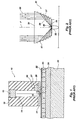
- a prior art near-field device 30 for emitting light energy through an aperture 31 having a diameter less than the wavelength of the light beam.
- This structure overcomes the diffraction limit for focusing light on an object, by generating an evanescent light field 32 in the vicinity of the aperture.
- the evanescent field protrudes from the aperture a short distance, resulting in the transfer of energy (evanescent coupling) with a storage medium 33 disposed at a distance of less than a wavelength of the light from the tip of the aperture.
- the prior art near-field device 30 is defined by an incident surface 34, a bottom surface 35 and a reflective side 37.
- the incident surface and the bottom surface are both generally flat and disposed parallel to each other.
- the reflective side 37 may be parabolic shaped and is coated with a reflective surface.
- a collimated laser beam 38 impinges upon the incident surface 34 and passes through to sides 37.
- the laser beam 38 is then reflected by the sides 37 as a focused beam 39 that impinges upon the bottom surface 35 at a focal spot 36.
- the focal spot is located along a central axis P in very close proximity to the storage medium 33, such that the localized evanescent light field 32 interacts with medium 33 to enable data to be transduced to and from storage medium 33 by near-field coupling.
- the present invention preferably uses a light sensitive medium in the storage areas of the storage layer that is susceptible to changing states in response to directed light beams.
- light beams includes evanescent fields generated by near-field optic systems.
- One preferred embodiment of the light sensitive medium is a material that changes between amorphous and crystalline in response to light beams, depending on the amount, intensity and duration of the light beam. A more detailed discussion of this state change in response to electron beams is given in U.S. Patent 5,557,596 (Gibson et al.).
- preferred materials include phase-change compounds incorporating the chalcogens S, Se, or Te.
- the medium may be capable of changing between different crystalline phases or between one chemical composition and another.
- state is meant to include different crystalline phases and the amorphous state, as well as variations in chemical composition, or morphology, or changes in the density, location or nature of trapped charges, or the density and type of defects that affect the relevant electrical properties.
- the medium also preferably has a characteristic of generating electron-hole pairs in at least one of the states when impacted by a directed light beam.
- the plurality of the states of the medium exhibit substantial differences in the activity of electron-hole carrier pairs that are generated during the read phase.
- This electron-hole carrier pair activity can be reflected in the amount of carriers that are initially generated by the light beam, and/or by the fraction of generated carriers that flow across a diode junction (diode embodiment), that recombine while emitting radiation (photoluminescent embodiment), or that change the effective conductivity of the storage medium (photoconductivity embodiment).
- each data storage area represented by its state
- the nature of the data stored in each data storage area is reflected in a substantial difference in the amount and the activity of electron-hole carrier pairs that are generated by a light beam directed at the medium during the read phase.
- the read light beam is directed at a lower level of intensity than the write light beam, so as to not cause unwanted writing in the storage areas.
- suitable materials for providing contrast between different states of the materials with regard to the activity of electron-hole carrier pairs for the three media types described herein would include various chalcogen-based compounds.
- a preferred embodiment of the present invention is shown in the form of a data storage system 40 utilizing a semiconductor diode 41.
- Light emitting devices 43 such as near-field optics systems, are disposed above a data storage layer 42 that comprises one layer of the diode 41.
- Layer 42 is disposed on an additional layer 44 to form the diode 41.
- the diode can be any type that provides a built-in field for separating charge carriers, such as a p-n junction, pin-junction or Schottky barrier device, depending on the materials used.
- a data bit is written by locally altering the state at areas 45 of the storage layer 42 with the use of light emitting units 43 emitting directed light beams 46 on storage areas 45 in storage layer 42.
- the different states of the storage areas 45 must provide a contrast in bit detection during the read function.
- the storage layer 42 may comprise a phase-change material as typically used in optical recording. These materials can be reversibly changed from crystalline to amorphous by applying heat at a pre-determined temperature profile over a preselected time period. The state may be changed from crystalline to amorphous by heating the area with a high intensity light beam, sufficient to melt the phase-change material, and then quickly decreasing the intensity of the beam to quench the area. Quenching a phase-change material causes it to cool rapidly into an amorphous state without time to anneal. The state of the storage area may be changed from amorphous to crystalline by using a light beam to heat the phase-change material just enough to anneal it.
- the materials may be changed from one crystalline state to another crystalline state using different temperatures for different time periods.
- the near-field evanescent light field can be regulated to apply the temperature-time profile and change the phase.
- Other sources of energy such as a resistive heater or applied electric or magnetic field may be used to bias a large area of the storage layer 42 to aid the light beams 46 in locally affecting a phase change in the storage areas 45.
- the light emitters 43 emit a lower level energy field to locally excite charge carriers in the storage area 45 of the diode 41. If carriers are excited in the storage layer 42, the number of carriers created (the "generation efficiency") will depend on the state of the storage areas 45 where the light beams 46 are incident. A factor that affects generation efficiency is the band structure of the storage layer. Some fraction of the generated carriers of one sign (electrons or holes) will be swept across the diode interface 47 (the "collection efficiency) under the influence of a built-in field. An additional field may be applied across interface 47 by a voltage source 48. The current that results from carriers passing across the diode interface 47 can be monitored by a detection signal 49 taken across the interface 47 to determine the state of data storage areas 45. The collection efficiency is dependent upon, among other things, the recombination rate and mobility in and around the area on which the read photons are incident and the effect of the built-in fields.
- phase-change material of storage layer 42 can be comprised of a number of phase change materials with the appropriate electrical properties (bandgap, mobility, carrier lifetime, carrier density, etc.)including a number of chalcogenide-based phase-change materials.
- Storage device 50 includes an electrically insulating substrate 52 and a photoconductive layer 54.
- the substrate 52 may be made of silicon having an oxidized top layer.
- the photoconductive layer 54 is disposed above the oxidized top layer and is preferably made of a chalcogenide-based phase change material having a high "dark" resistivity when not impinged upon by an energy beam.
- the photoconductive layer 54 may include a single layer of photoconductive material, multiple layers of the same type of photoconductive material or multiple layers of different photoconductive materials.
- a plurality of spaced apart electrodes make contact with the same photoconductive layer 54.
- the photoconductive material of layer 54 may be deposited over or under electrodes 56 and 57.
- a data storage region is located between electrodes 56 and 57, including multiple spaced-apart data storage areas 58, as shown in Figure 4.
- the storage areas may be arranged in rows and columns, with the state of each area being determinative of the data stored therein.
- the storage areas are of submicrometre size, approximately 10 nanometers to 30 nanometers in diameter and spaced about 50 nanometers apart.
- An array of light beam emitters 59 is disposed above the photoconductive layer 54.
- the light beam emitter 59 is a near-field optics device emitting an evanescent light field, as discussed above.
- the electron beam 55 has appropriate time and power parameters to change the state of the storage areas 58 between amorphous and crystalline states or between different crystalline states, as discussed above.
- a constant current or voltage source 60 may be used to regulate the intensity of the light beam 59.
- Micromovers are preferably used to scan the array of light beam emitters over the storage areas 58, as described in U.S. Patent 5,986,381.
- a power supply 62 applies a bias voltage across the electrodes 56 and 57 during the read function. This bias voltage induces an electric field 64 in the plane of the photoconductive layer 54.
- the power supply may be fabricated on the substrate 52 or may be provided outside the chip.
- light beam 59 is scanned between electrodes 56 and 57 while the bias voltage is applied to the electrodes.
- the light beam 59 impacts a storage area 58, electron carriers and hole carriers are produced and accelerated by the electric field 56 towards electrodes 56 and 57.
- This movement of electrons and holes causes a current to flow, which is detected by a read circuit 66 to provide an output signal 68.
- the rate at which electrons and holes are generated depends upon the state of the storage areas 58. If a phase-change material is used, a contrast in photocurrent magnitude results from the difference in material properties between written and unwritten areas.
- Geminate recombination rate means the rate at which initially created electron-hole pairs recombine before they are separated into free carriers.
- Further current magnitude contrast may be obtained from differences in the lifetime or mobility of the free carriers for written and unwritten areas. For example, in general, the mobility will be lower and carrier lifetime will be shorter in an amorphous material than in a crystalline material. Additional contrasts may arise from differences in resistivity and effects at the interface between written and unwritten areas such as the creation of built-in fields. By monitoring the changes in the magnitude of the photocurrent, the states of the storage areas 58 can be determined.
- the output 68 from read circuit 66 may be amplified and converted from analog to a digital value if desired.
- the storage layer is a photoluminescent material in one of its states or potentially in more than one of its states if multibit recording is used.
- the photo-luminescent material could have different luminescent properties in each of its states.
- the material could luminesce at different wavelengths in each state.
- a photo-detector such as a photodiode or microfabricated photomultiplier tube may be used for photon detection.
- a photodiode has a photodiode interface 72 between upper layer 71 and lower layer 73.
- a storage layer 74 composed of photoluminescent material is deposited on the surface of upper layer 71.
- Light emitters 76 are disposed near the surface of storage layer 74 to direct light beams 78 onto the surface.
- Preferably near-field light sources are used, as described above.
- the photoluminescent material can be any one of a number of chalcogenide-based phase-change materials.
- the light emitting properties may be altered in a number of different ways, such as by changing the electronic band structure, i.e., from a direct band gap material to an indirect band gap material, by altering the ratio of the non-radiative to radiative recombination rates, or by changing the wavelength or escape efficiency of the light emitted by the material.
- the light beams 78 have a lower power intensity to prevent undesired writing.
- the written storage areas 79 will emit a different number of photons than the other areas on the storage layer 74 that have not been written.
- the emitted photons will generate a current of electron and hole carriers in the photodiode, some of which will cross the photodiode interface 72.
- a meter 75 connected between the layers of photodiode 70 measures the current or voltage across the photodiode interface 72 as each storage area is impacted by a light beam to determine whether each storage area has been altered to store data bits.
- top and bottom electrodes will enhance the uniformity of the biasing field formed between the top electrode and the storage layer.
- a back electrode could be present, either on the side of the substrate opposite the optical sources, if a conducting substrate is used, or on top of the substrate, if an electrically isolated substrate is used that provides mechanical support only.
- a top electrode can be used that covers the entire top surface of the device.
- the storage layer may also be covered with a protective layer to prevent chemical changes, such as oxidation or thermo-mechanical changes such as bump or pit formation, during the write mode, as long as it is thin enough to allow writing of small bits.
- the protective layer may be merely a passivation layer or a conducting transparent electrode that is used to collect the photo-generated carriers.
- the storage layer may also be covered with a layer that enhances thermal properties of the overall storage medium.
- a layer that enhances thermal quenching by acting as a heat sink when changing the state of the materials to an amorphous state.
- a cover layer it may be desirable to have a layer underneath the storage layer or adjacent layer that improves thermal properties, such as the ability to quench and amorphize the storage layer.
- a protective underlayer may also enhance the robustness of the device by preventing interdiffusion between the storage layer and the substrate material, or by discouraging delamination or dewetting of the storage layer from the substrate.
- a layer covering the storage layer may also be used to enhance optical properties, such as an anti-reflection coating.
- a coating could be used to increase the amount of light from the light source that is absorbed in the storage layer or the adjacent layer.
- a layer underneath the storage layer could be used to enhance optical properties.
- the light beam may be varied as needed.
- the light beam may be applied in a constant mode, with the light source on continually and the sampling window provided by translation or rotation of the media beneath the source.
- the optical source might be pulsed or otherwise modulated to use a phase-selective or frequency-selective signal-to-noise enhancement technique in the diode signal amplifier electronics.
Landscapes
- Optical Recording Or Reproduction (AREA)
- Optical Head (AREA)
- Optical Record Carriers And Manufacture Thereof (AREA)
Abstract
Description
and the storage layer. A back electrode could be present, either on the side of the substrate opposite the optical sources, if a conducting substrate is used, or on top of the substrate, if an electrically isolated substrate is used that provides mechanical support only. Using an optical beam, a top electrode can be used that covers the entire top surface of the device.
Claims (10)
- A data storage unit, including:a data storage layer (42) having a plurality of data storage areas (45) for storing and reading data thereon during read and write phases, respectively;an array of directed light beam emitters (43) in close proximity to the data storage layer (42) for selectively directing a first light beam (46) to the data storage layer (42) to write data in certain data storage areas (45) during the write phase and for selectively directing a second light beam (46) to the data storage layer (42) to read data in certain data storage areas (45) during a read phase;a medium disposed on the data storage areas (45) that changes between a plurality of states in response to the first directed light beam (46) during the write phase, and that generates electron-hole pairs in response to the second directed light beam (46) during the read phase, the plurality of states exhibiting substantial differences in the activity of electron-hole carrier pairs generated in response to the second directed light beam (46);a detection region (41) in communication with the data storage areas (45) for determining the activity of the electron-hole pairs during the read phase, the activity of electron-hole pairs being relative to the state of each storage areas (45); anda detector (48) associated with the detection region (41) for measuring the activity of the electron-hole carrier pairs to determine the data stored in the data storage areas (45).
- A data storage unit as recited in claim 1, wherein the array of light beam emitters (43) includes near-field light emitters for selectively directing an evanescent field from the light emitters (43) onto the data storage layer (42) to write data into the data storage areas (45) and to read said data.
- A data storage unit as recited in claim 1 or 2, wherein the detection region is the junction (47) of a semiconductor diode (41) and the activity of the electron-hole carrier pairs comprises the amount of electron-hole carrier pairs that flow across the junction (47) of the semiconductor diode (41).
- A data storage unit as recited in claim 1, 2 or 3, wherein the region for detecting the electron-hole carrier pair activity comprises a photoconductivity region (50) having a photoconductive material and two electrodes (56, 57) with a potential across the two electrodes to direct the carrier flow between the electrodes (56, 57) in the photoconductive material.
- A data storage unit as recited in any preceding claim, wherein the medium is a photo-luminescent material (74) responsive to the second light beam (78) for generating photon emissions in response to the recombination of the electron-hole carrier pairs generated during the read phase.
- A data storage unit as recited in any preceding claim, wherein the medium comprises a material susceptible to changing states in response to the first directed light beam.
- A method of writing and reading data in a data storage unit (40) including a data storage layer (42) having a plurality of data storage areas (45) with a medium disposed thereon that is susceptible to changing states in response to light beam energy (46) for storing and reading data thereon during read and write phases, respectively, including the steps of:selectively directing a first light beam (46) to the medium to write data in certain data storage areas (45) during the write phase by changing states of the medium using light beam emitters (43) in close proximity to the data storage layer;selectively directing a second light beam (46) to the medium on the data storage areas (45) to read data in certain data storage areas (45) during the read phase by generating electron-hole pairs, the activity of the electron-hole pairs being relative to the state of the medium;determining the activity of the electron-hole pairs during the read phase, the activity being in a detection region (41) in communication with the data storage areas (45), the activity of electron-hole pairs being dependent on the state of each of the data storage areas (45); andmeasuring the amount of electron-hole carrier pair activity in the detection region (41) to detect the presence of data bits in the storage areas (45).
- A method as recited in claim 7, wherein the step of selectively directing first and second light beams includes:arranging an array of near-field light emitters (43) spaced less than a light wavelength from the data storage layer (42);generating from the near-field light emitters (43) a plurality of evanescent light fields (46) in contact with the data storage layer to write the data on the medium in the data storage areas (45) during the write phase and to read the data from the data storage areas (45) during the read phase.
- A method as recited in claim 7 or 8, wherein the electron-hole carrier pair activity is generated by carriers generated in the data storage layer (42) in response to light from the light means (46).
- A method as recited in claim 7 or 8, wherein the electron-hole carrier pair activity is generated by photons generated in the data storage layer (54) in response to light from the light beams (55).
Applications Claiming Priority (2)
| Application Number | Priority Date | Filing Date | Title |
|---|---|---|---|
| US865940 | 2001-05-25 | ||
| US09/865,940 US6970413B2 (en) | 2001-05-25 | 2001-05-25 | Data storage medium utilizing directed light beam and near-field optical sources |
Publications (2)
| Publication Number | Publication Date |
|---|---|
| EP1260975A2 true EP1260975A2 (en) | 2002-11-27 |
| EP1260975A3 EP1260975A3 (en) | 2004-05-06 |
Family
ID=25346568
Family Applications (1)
| Application Number | Title | Priority Date | Filing Date |
|---|---|---|---|
| EP02253366A Withdrawn EP1260975A3 (en) | 2001-05-25 | 2002-05-14 | Data storage medium |
Country Status (4)
| Country | Link |
|---|---|
| US (1) | US6970413B2 (en) |
| EP (1) | EP1260975A3 (en) |
| JP (1) | JP2003030832A (en) |
| CN (1) | CN1263002C (en) |
Cited By (1)
| Publication number | Priority date | Publication date | Assignee | Title |
|---|---|---|---|---|
| WO2004112046A1 (en) * | 2003-06-12 | 2004-12-23 | Hewlett-Packard Development Company, L.P. | Data storage medium having layers acting as transistor when illuminated |
Families Citing this family (16)
| Publication number | Priority date | Publication date | Assignee | Title |
|---|---|---|---|---|
| US6847045B2 (en) * | 2001-10-12 | 2005-01-25 | Hewlett-Packard Development Company, L.P. | High-current avalanche-tunneling and injection-tunneling semiconductor-dielectric-metal stable cold emitter, which emulates the negative electron affinity mechanism of emission |
| US7106622B2 (en) * | 2002-01-09 | 2006-09-12 | Intel Corporation | Phase-change memory device capable of preprogramming memory cells optically and reading/writing memory cells electrically |
| US7027380B2 (en) * | 2002-05-02 | 2006-04-11 | Hewlett-Packard Development Company, L.P. | Atomic resolution storage device |
| US7519373B2 (en) * | 2002-08-29 | 2009-04-14 | Andrew Llc | System and method for geo-location of mobile appliances using diverse standard tasking and reporting |
| WO2004077414A1 (en) * | 2003-02-27 | 2004-09-10 | Koninklijke Philips Electronics N.V. | Multi-stack rolled-up information carrier |
| NL1022855C2 (en) * | 2003-03-05 | 2004-09-07 | Univ Delft Tech | Method and device for the controlled manufacture of openings on a nanometer scale. |
| CN1689092A (en) * | 2003-03-28 | 2005-10-26 | 富士通株式会社 | Light irradiation head and information storage device |
| US7239599B2 (en) | 2003-03-28 | 2007-07-03 | Fujitsu Limited | Light irradiation head and information storage apparatus |
| US20040218499A1 (en) * | 2003-05-01 | 2004-11-04 | Alison Chaiken | Ultra-high density storage and retrieval device using ordered-defect materials and methods of fabrication thereof |
| US6979838B2 (en) * | 2003-09-03 | 2005-12-27 | Hewlett-Packard Development Company, L.P. | Ultra-high density storage device using phase change diode memory cells and methods of fabrication thereof |
| US7057202B2 (en) | 2003-09-26 | 2006-06-06 | Hewlett-Packard Development Company, L.P. | Ultra-high density storage device using phase change diode memory cells and methods of fabrication thereof |
| US7616551B2 (en) * | 2003-11-25 | 2009-11-10 | Samsung Electronics Co., Ltd. | Molecular optoelectronic memory device |
| US7596072B2 (en) * | 2004-12-22 | 2009-09-29 | Seagate Technology Llc | Optical recording using a waveguide structure and a phase change medium |
| US20060233091A1 (en) * | 2005-04-01 | 2006-10-19 | Schut David M | Storage device having storage cells having a size less than a write light wavelength |
| US8339905B2 (en) * | 2005-04-13 | 2012-12-25 | Seagate Technology Llc | Alignment features for heat assisted magnetic recording transducers |
| DE102022113005A1 (en) * | 2022-05-24 | 2023-11-30 | Syntegon Technology Gmbh | Transport system for sterile tubes and use of a transport system |
Family Cites Families (15)
| Publication number | Priority date | Publication date | Assignee | Title |
|---|---|---|---|---|
| US4213192A (en) * | 1979-01-15 | 1980-07-15 | Christensen Alton O Sr | Electron beam accessed read-write-erase random access memory |
| EP0363147B1 (en) * | 1988-10-04 | 1996-06-05 | Canon Kabushiki Kaisha | Recording and reproducing apparatus and recording and reproducing method and recording medium for the recording and reproducing method |
| US5270995A (en) * | 1989-01-13 | 1993-12-14 | Sharp Kabushiki Kaisha | Method for recording and reproducing information by varying a work function of a recording medium and device for the same |
| US5675532A (en) * | 1994-07-28 | 1997-10-07 | Kabushiki Kaisha Toshiba | Recording medium and recording/reproduction method |
| US5615143A (en) * | 1994-09-19 | 1997-03-25 | Cornell Research Foundation, Inc. | Optomechanical terabit data storage system |
| US5557596A (en) * | 1995-03-20 | 1996-09-17 | Gibson; Gary | Ultra-high density storage device |
| US5808973A (en) * | 1995-09-06 | 1998-09-15 | Kabushiki Kaisha Toshiba | Near field recording and reproducing apparatus |
| JP3618896B2 (en) * | 1996-03-29 | 2005-02-09 | キヤノン株式会社 | Manufacturing method of probe having minute aperture, probe thereby, combined apparatus of scanning near-field light microscope and scanning tunneling microscope using the probe, and recording / reproducing apparatus using the probe |
| JP3697034B2 (en) * | 1997-08-26 | 2005-09-21 | キヤノン株式会社 | Method of manufacturing protrusions having minute openings, and probes or multiprobes using them |
| JPH11166935A (en) * | 1997-09-25 | 1999-06-22 | Canon Inc | Optical probe for light detection or irradiation, near-field optical microscope equipped with the probe, method for manufacturing the optical probe, and substrate used for the manufacturing |
| JP3519623B2 (en) * | 1998-03-13 | 2004-04-19 | 株式会社東芝 | Recording medium and method for manufacturing the same |
| US6185051B1 (en) * | 1999-06-23 | 2001-02-06 | Read-Rite Corporation | High numerical aperture optical focusing device for use in data storage systems |
| JP3688530B2 (en) * | 1999-09-29 | 2005-08-31 | 株式会社東芝 | Recording medium, recording apparatus, and recording method |
| US6473388B1 (en) * | 2000-08-31 | 2002-10-29 | Hewlett Packard Company | Ultra-high density information storage device based on modulated cathodoconductivity |
| US6643248B2 (en) * | 2001-04-16 | 2003-11-04 | Hewlett-Packard Development Company, L.P. | Data storage device |
-
2001
- 2001-05-25 US US09/865,940 patent/US6970413B2/en not_active Expired - Fee Related
-
2002
- 2002-05-14 EP EP02253366A patent/EP1260975A3/en not_active Withdrawn
- 2002-05-27 JP JP2002152757A patent/JP2003030832A/en not_active Withdrawn
- 2002-05-27 CN CNB021220352A patent/CN1263002C/en not_active Expired - Fee Related
Cited By (1)
| Publication number | Priority date | Publication date | Assignee | Title |
|---|---|---|---|---|
| WO2004112046A1 (en) * | 2003-06-12 | 2004-12-23 | Hewlett-Packard Development Company, L.P. | Data storage medium having layers acting as transistor when illuminated |
Also Published As
| Publication number | Publication date |
|---|---|
| US6970413B2 (en) | 2005-11-29 |
| EP1260975A3 (en) | 2004-05-06 |
| CN1391214A (en) | 2003-01-15 |
| US20020176349A1 (en) | 2002-11-28 |
| JP2003030832A (en) | 2003-01-31 |
| CN1263002C (en) | 2006-07-05 |
Similar Documents
| Publication | Publication Date | Title |
|---|---|---|
| US6970413B2 (en) | Data storage medium utilizing directed light beam and near-field optical sources | |
| US6975575B2 (en) | Data storage media and methods utilizing a layer adjacent the storage layer | |
| US6507552B2 (en) | AFM version of diode-and cathodoconductivity-and cathodoluminescence-based data storage media | |
| US6473388B1 (en) | Ultra-high density information storage device based on modulated cathodoconductivity | |
| JP2001101708A (en) | Recording medium, recording device and recording method | |
| US6125095A (en) | Luminescent recording layer holding a plurality of positive or negative charges | |
| US8050150B2 (en) | Near-field light detection element and information reproducing medium reproducing method | |
| JP2003030832A5 (en) | ||
| US5038321A (en) | Eraseable electro-optic storage disk, method of and apparatus for recording and reading data therefor | |
| US7239600B2 (en) | Storage device based on phase-change modulated luminescence | |
| US7082095B2 (en) | System and method for storing data | |
| US6469292B1 (en) | Photodetector and method of driving the same | |
| US7170771B2 (en) | Method of reading a data bit including detecting conductivity of a volume of alloy exposed to an electron beam | |
| KR100497419B1 (en) | An information storage medium and an optical device using the medium | |
| EP1014345B1 (en) | Optical recording / reproducing method and recording medium used for optical recording and reproduction | |
| KR930007179B1 (en) | Information recording and reproducing method and apparatus thereof | |
| JP2002082414A (en) | Optical recording medium as well as reproducing method and reproducing device for the same | |
| JP4211111B2 (en) | Optical head | |
| Kim et al. | Simple Near‐Field Optical Recording Using Bent Cantilever Probes | |
| JP4381540B2 (en) | Reproduction method of optical recording medium | |
| JP2002312986A (en) | Optical recording medium, processing apparatus and processing method thereof | |
| GB2424735A (en) | Phase change memory device written to using a laser with a wavelength larger than the memory cells |
Legal Events
| Date | Code | Title | Description |
|---|---|---|---|
| PUAI | Public reference made under article 153(3) epc to a published international application that has entered the european phase |
Free format text: ORIGINAL CODE: 0009012 |
|
| AK | Designated contracting states |
Kind code of ref document: A2 Designated state(s): AT BE CH CY DE DK ES FI FR GB GR IE IT LI LU MC NL PT SE TR |
|
| AX | Request for extension of the european patent |
Free format text: AL;LT;LV;MK;RO;SI |
|
| PUAL | Search report despatched |
Free format text: ORIGINAL CODE: 0009013 |
|
| AK | Designated contracting states |
Kind code of ref document: A3 Designated state(s): AT BE CH CY DE DK ES FI FR GB GR IE IT LI LU MC NL PT SE TR |
|
| AX | Request for extension of the european patent |
Extension state: AL LT LV MK RO SI |
|
| 17P | Request for examination filed |
Effective date: 20040614 |
|
| AKX | Designation fees paid |
Designated state(s): DE GB |
|
| STAA | Information on the status of an ep patent application or granted ep patent |
Free format text: STATUS: THE APPLICATION HAS BEEN WITHDRAWN |
|
| 18W | Application withdrawn |
Effective date: 20060509 |