EP1260908A2 - Data transfer control device, electronic equipment, and data transfer control method - Google Patents
Data transfer control device, electronic equipment, and data transfer control method Download PDFInfo
- Publication number
- EP1260908A2 EP1260908A2 EP02010402A EP02010402A EP1260908A2 EP 1260908 A2 EP1260908 A2 EP 1260908A2 EP 02010402 A EP02010402 A EP 02010402A EP 02010402 A EP02010402 A EP 02010402A EP 1260908 A2 EP1260908 A2 EP 1260908A2
- Authority
- EP
- European Patent Office
- Prior art keywords
- data
- bus
- storage area
- data storage
- transfer
- Prior art date
- Legal status (The legal status is an assumption and is not a legal conclusion. Google has not performed a legal analysis and makes no representation as to the accuracy of the status listed.)
- Granted
Links
Images






Classifications
-
- G—PHYSICS
- G06—COMPUTING OR CALCULATING; COUNTING
- G06F—ELECTRIC DIGITAL DATA PROCESSING
- G06F13/00—Interconnection of, or transfer of information or other signals between, memories, input/output devices or central processing units
- G06F13/38—Information transfer, e.g. on bus
-
- G—PHYSICS
- G06—COMPUTING OR CALCULATING; COUNTING
- G06F—ELECTRIC DIGITAL DATA PROCESSING
- G06F13/00—Interconnection of, or transfer of information or other signals between, memories, input/output devices or central processing units
- G06F13/38—Information transfer, e.g. on bus
- G06F13/382—Information transfer, e.g. on bus using universal interface adapter
- G06F13/385—Information transfer, e.g. on bus using universal interface adapter for adaptation of a particular data processing system to different peripheral devices
-
- G—PHYSICS
- G06—COMPUTING OR CALCULATING; COUNTING
- G06F—ELECTRIC DIGITAL DATA PROCESSING
- G06F13/00—Interconnection of, or transfer of information or other signals between, memories, input/output devices or central processing units
- G06F13/14—Handling requests for interconnection or transfer
- G06F13/20—Handling requests for interconnection or transfer for access to input/output bus
- G06F13/28—Handling requests for interconnection or transfer for access to input/output bus using burst mode transfer, e.g. direct memory access DMA, cycle steal
-
- G—PHYSICS
- G06—COMPUTING OR CALCULATING; COUNTING
- G06F—ELECTRIC DIGITAL DATA PROCESSING
- G06F13/00—Interconnection of, or transfer of information or other signals between, memories, input/output devices or central processing units
- G06F13/38—Information transfer, e.g. on bus
- G06F13/40—Bus structure
- G06F13/4004—Coupling between buses
- G06F13/4027—Coupling between buses using bus bridges
Definitions
- the present invention relates to a data transfer control device, electronic equipment, and a data transfer control method.
- USB universal serial bus
- this USB standard In comparison with the IEEE 1394 standard, which is also attracting notice as a standard for the same serial bus interface, this USB standard has a problem in that the transfer speed thereof is slower.
- USB 2.0 which can implement a data transfer speed of 480 Mbps (in HS mode), far faster than that of the previous USB 1.1 standard, while maintaining backward compatibility with USB 1.1.
- USB 2.0 data transfer is performed at 480 Mbps in high-speed (HS) mode. It therefore has the advantage of enabling its use as an interface for a storage device such as a hard disk drive or optical disk drive, which requires fast transfer speeds.
- the data transfer control device connected to the USB bus has to process the data that is transferred at the high speed of 480 Mbps. If the processing speed of the data transfer control device or the firmware (CPU) that controls the data transfer control device is slow, it is not possible to ensure the effective transfer speed and a problem occurs in that the bus zone could be lost.
- a data transfer control device for data transfer through a bus.
- the data transfer control device comprises:
- the present invention makes it possible to determine the end of a data phase (data transport: transfer of all the data) during data transfer in a first direction, on condition that data transmission (such as DMA transfer) through the second bus has ended.
- data transport transfer of all the data
- the end of the data phase is determined on condition that data reception through the second bus has ended and the data storage area has subsequently become empty.
- the data transfer control device may further comprise a counter which counts the size of data transmitted or received through the second bus.
- the status of the data reception through the second bus may be acquired, and the thus-acquired status may be transmitted though the first bus during a status phase after the end of the data phase.
- a short packet in the data storage area may be automatically transmitted through the first bus, when data reception through the second bus ends and also the size of data remaining in the data storage area of the buffer is less than the maximum packet size.
- This enables the automatic transmission of a short packet in the data storage area by hardware, without involving the processing unit. This makes it possible to reduce the processing load on the processing unit, enabling an increase in the effective transfer speed.
- the data transfer control device may further comprise a unit which sets the automatic transmission of a short packet from the data storage area to either enabled or disabled.
- the automatic transmission may be set to be disabled when data that has been received through the second bus has given information and is transmitted through the first bus.
- a processing unit may be notified of the presence of a short packet in the data storage area, when data reception through the second bus ends and also the size of data remaining in the data storage area of the buffer is less than the maximum packet size.
- information that has been input first to the data storage may be output first from the data storage area.
- DMA direct memory access
- data transfer may be in accordance with the universal serial bus (USB) standard.
- USB universal serial bus
- Electronic equipment in accordance with the present invention comprises any of the above described data transfer control devices; and a device which performs output processing, fetch processing, or storage processing on data transferred through the data transfer control device and the bus.
- this invention makes it possible to reduce the processing load on the processing unit (such as the firmware) that controls the data transfer of the data transfer control device, it enables benefits such as reductions in the cost and scale of electronic equipment.
- USB USB 2.0
- USB differs from other methods such as IEEE 1394 in that a host takes the initiative. In other words, activation of a data transfer transaction is done by the host side and the greater part of control relating to data transfer is done by the host. This increases the processing load on the host, but since the personal computer (PC) that forms the host has a high-speed, high-performance CPU (processor), the processing of such a heavy load is not too much of a problem.
- PC personal computer
- the processing and configuration on the device side can be simplified. It is therefore not necessary to use a high-performance, fast CPU on the device side, such as the host, making it possible to use an inexpensive CPU (microprocessor), thereby reducing costs.
- end points EPO to EP15
- FIFO buffer
- Each of these end points can be addressed uniquely by a device address and an end point number.
- the host can freely perform data transmission to a desired end point or data reception from a desired end point, by specifying a device address and an end point number.
- End point specification is done freely by the device side, and the host can be notified of details such as the allocation of end point numbers and the sizes of storage areas allocated to those end points, during enumeration processing.
- USB provides control transfer, isochronous transfer, interrupt transfer, and bulk transfer as data transfer types.
- control transfer is a transfer mode for control performed through a control end point between the host and the device (target).
- This control transfer sends information such as configuration information for initializing the device.
- Isochronous transfer is a transfer mode that is provided for transferring data where it is more important to ensure bandwidth rather than correctness, such as image data or audio data. Since this isochronous transfer ensures that a fixed quantity of data can be transferred in a fixed period, it is an effective transfer mode for applications where real-time data capabilities are important.
- Interrupt transfer is a transfer mode that is provided for transferring a small quantity of data at a comparatively low transfer speed.
- Bulk transfer is a transfer mode that is provided for transferring a large quantity data that occurs at irregular periods. This bulk transfer enables data transfer at spare times other than times being used by isochronous transfers or interrupt transfers, and also enables checking of the correctness of the data. It is therefore an effective transfer mode for data transfer where real-time capabilities are not important but data reliability can be ensured.
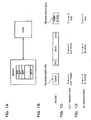
- a transaction in USB bulk transfer mode is basically made up of three packets as shown in Fig. 1B: a token packet, a data packet, and a handshake packet. Note that a handshake packet is not necessary with isochronous transfer.
- a token packet is a packet that is used in situations such as when the host requests a read or write with respect to an end point of the device (target) .
- This token packet has fields such as PID (a packet ID such as OUT, IN, SOF, or SETUP), ADDR (device address), ENDP (end point number), and CRC (Cyclic Redundancy Check), by way of example.
- PID a packet ID such as OUT, IN, SOF, or SETUP
- ADDR device address
- ENDP end point number
- CRC Cyclic Redundancy Check
- a data packet is a packet for sending the actual data, and has PID (DATA0, DATA1), DATA (the actual data), and CRC fields.
- a handshake packet is a packet used by the reception side to inform the transmitter side whether or not data reception was successful, and has a PID (ACK, NAK, or STALL) field.
- the host With an OUT transaction (a transaction whereby the host outputs information to the device), the host first sends an OUT token packet to the device, as shown in Fig. 1C. The host then sends an OUT data packet to the device. If the device succeeds in receiving the OUT data packet, it sends an ACK handshake packet to the host.
- OUT transaction a transaction whereby the host outputs information to the device
- the host With an IN transaction (a transaction whereby the host inputs information from the device), on the other hand, the host first sends an IN token packet to the device, as shown in Fig. 1D. On receiving the IN token packet, the device sends an IN data packet to the host. If the host succeeds in receiving the IN data packet, it sends an ACK handshake packet to the device.
- IN transaction a transaction whereby the host inputs information from the device
- USB devices are divided into a number of classes.
- Devices such as hard disk drives and optical disk drives belong to a class called mass storage, and there are specifications created by the vendors of electronic equipment within this mass storage class, such as control/bulk/interrupt (CBI) and Bulk-Only specifications.
- CBI control/bulk/interrupt
- the device provides end points EP0 EP1, EP2, and EP3 for control, bulk-out, bulk-in, and interrupt, as shown in Fig. 2A.
- the end point EP0 is for the transfer of USB-layer control packets or command packets.
- EP1 is for the transfer of OUT data (data transferred from the host to the device),
- EP2 is for the transfer of IN data (data transferred from the device to the host),
- EP3 is for the transfer of interrupt IN packets.
- any of EP1 to EP15 can be allocated as bulk-out, bulk-in, and interrupt IN end points, from the device side.
- the device provides end points EP0 EP1, and EP2 for control, bulk-out, and bulk-in, as shown in Fig. 2B.
- the end point EP0 is for the transfer of USB-layer control packets.
- EP1 is for the transfer of commands (CBW) and OUT data, and EP2 is for the transfer of statuses (CSW) and IN data packets.
- CBW commands
- CSW statuses
- any of EP1 to EP15 can be set to be bulk-out and bulk-in end points, from the device side.
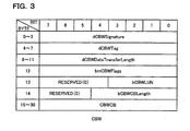
- a command block wrapper is a packet that includes a command block and information relating to the command block, and has the format shown in Fig. 3.
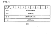
- a command status wrapper is a packet that includes the status of a command block, and has the format shown in Fig. 4.
- dCBWSignature is information for identifying that packet as a CBW
- dCBWTag is a command block tag
- dCBWDataTransferLength specifies the length of data to be transferred in the data phase.
- the bmCBWFlags field is a flag for specifying the transfer direction or the like
- dCBWLUN is a logical unit number
- bCBWCBLength is the command length
- CBWCB is a command block in which an ATA/ATAPI or SCSI command is encapsulated and described.
- dCSWSignature is information for identifying that packet as a CSW
- dCSWTag is a status block tag
- the value of the dCBWTag of the CBW corresponding to that CSW is written therein.
- the CSWDataResidue field gives the difference between the length of data specified by dCBWDataTransferLength of the CBW and the length of data that the device has actually processed
- bCSWStatus is a status block.
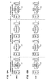
- the host When the host writes data to the device, it first performs a command phase (command transport) in which it transfers a CBW to the device, as shown in Fig. 5A. More specifically, the host transfers a token packet specifying the end point EP1 to the device, then transfers a CBW (see A1 in Fig. 2B and Fig. 3) to the end point EP1 of the device. This CBW comprises a write command. If the device returns a handshake (H.S) to the host, the command phase ends.
- command transport command transport
- the host transfers a token packet specifying the end point EP1 to the device, then transfers a CBW (see A1 in Fig. 2B and Fig. 3) to the end point EP1 of the device.
- This CBW comprises a write command.
- H.S handshake
- the data phase (data transport) starts.
- the host first transfers a token packet specifying the end point EP1 of the device, then it transfers OUT data (see A2 in Fig. 2B) to the end point EP1 of the device.
- Each transaction ends when an ACK handshake is returned from the device to the host. Transactions are repeated in this manner and the data phase ends when data has been transferred up to the data length specified in dCBWDataTransferLength of the CBW (see Fig. 3).
- a status phase (status transport) starts.
- the host first transfers a token packet specifying the end point EP2 to the device.
- the device transfers the CSW that is at the end point EP2 (see A3 in Fig. 2B and Fig. 4) to the host.
- the status phase ends when an ACK handshake is returned from the host to the device.
- the host When the host reads data, it first transfers a token device specifying the end point EP1 to the device, then it transfers the CBW to the end point EP1 to the device.
- This CBW comprises a read command. If a handshake returns from the device to the host, the command phase ends.
- the data phase starts.
- the host first transfers a token packet specifying the end point EP2 to the device.
- the device transfers the IN data that is at the end point EP2 (see A4 in Fig. 2B) to the host, and one transaction ends. Transactions are repeated in this manner and the data phase ends when data has been transferred up to the data length specified in dCBWDataTransferLength of the CBW.
- the status phase starts.
- the processing in this status phase is similar to that of data write processing described with reference to Fig. 5A.
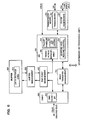
- FIG. 6 A configuration of the data transfer control device according to one embodiment of the present invention is shown in Fig. 6.
- the data transfer control device of this embodiment comprises a transceiver macro 20, an SIE 30, an end point management circuit 40, a buffer management circuit 50, a buffer 60, a bulk transfer management circuit 70, and a DMAC 80. Note that not all of the circuit blocks shown in Fig. 6 are necessary for the data transfer control device of the present invention, and thus some of them could be omitted.
- the transceiver macro 20 is a circuit for implementing data transfer in FS mode or HS mode by USB (the first bus) .
- This transceiver macro 20 comprises a transceiver circuit 22 and a clock generation circuit 24.
- the transceiver circuit 22 comprises an analog front-end circuit (reception and transmission circuitry) for transmitting and receiving data by USB (a first bus), using difference signals DP and DM. It also comprises circuitry for processing such as bit stuffing, bit unstuffing, serial-to-parallel conversion, parallel-to-serial conversion, NRZI decoding, NRZI encoding, and sampling clock generation.
- the clock generation circuit 24 is a circuit for generating clocks such as those used in the generation of the operating clock or sampling clock used by the data transfer control device, and comprises components such as PLLs and oscillation circuits for generating 480-MHz and 60-MHz clocks.
- a serial interface engine is a circuit for performing various types of processing such as USB packet transfer processing, and it comprises a packet handler circuit 32, a suspend-and-resume control circuit 34, and a transaction management circuit 36.
- the packet handler circuit 32 is a circuit for assembling (creating) or analyzing packets formed of headers and data, and it comprises a CRC processing circuit 33 that generates and decodes CRCs.
- the suspend-and-resume control circuit 34 is a circuit for sequence control during the suspension and resumption of processing.
- the transaction management circuit 36 is a circuit for managing transactions made up of token, data, handshake, and other packets. More specifically, when a token packet is received, this circuit confirms whether or not it has the device's own address and, if it does have that address, it performs processing to transfer packets to or from the host, then processing for transferring a handshake packet.
- the end point management circuit 40 is a circuit for managing the end points that form entrances to the various storage areas of the buffer, and it comprises components such as registers (a register set) for storing attribute information for those end points.
- the buffer management circuit 50 is a circuit for managing the buffer 60, and is formed of components such as RAM. More specifically, it generates write addresses or read addresses and performs processing to write data to the buffer 60 or read data from the buffer 60.
- the buffer 60 (packet storage means) is designed to store data (packets) temporarily, for transfer through USB, and it has various functions such as compensating for any speed difference between the data transfer speed of USB (the first bus) and the data transfer speed of EBUS (the second bus, or DMA bus).
- EBUS is an external bus that connects together devices such as hard disk drives, CD drives, and scanners.
- the buffer 60 has a data storage area 62 (FIFO: a storage area set to FIFO) for storing data (OUT data) to be received through USB (a first bus) and transmitted through EBUS (a second bus) during data transfer in a first direction (OUT transaction), and data (IN data) to be received through EBUS and transmitted through USB during data transfer in a second direction (IN transaction).
- FIFO data storage area 62
- the data transfer control device of this embodiment also determines that a data phase (data transport: the transfer of all the data) has ended during data transfer in the first direction, on condition that data transmission through EBUS has ended. Similarly, it determines that the data phase has ended during data transfer in a second direction, on condition that data reception via EBUS has ended and the data storage area 62 of the buffer 60 has become empty (an acknowledgment concerning the final-data packet has been returned through USB).
- a data phase data transport: the transfer of all the data
- the data transfer control device of this embodiment automatically transfers a short packet (a packet of a size that is less than the maximum packet size) of the data storage area 62 through USB, and CPU (firmware or processing unit) is notified of the presence of the short packet by an interrupt signal or the like.
- a command storage area (first storage area) for command blocks and a data storage area (second storage area) for data are provided on the buffer 60 for when a command block (first information) and data (second information: OUT data) have been allocated (see A1 and A2 of Fig. 2B) as information to be transferred through one end point (EP1 of Fig. 2B).
- the buffer management circuit 50 takes the information that is to be transferred from the host to the end point (EP1) and writes it to a command storage area for the command block.
- the data phase (second phase) in which data (OUT data) is transferred through USB, it takes the information that is to be transferred from the host to the end point and writes it to a data storage area for data. In other words, it switches the write area for information (command block or data) on condition that the phase has switched.
- this embodiment of the present invention could be configured in such a manner that a data storage area (third storage area) for data and a status storage area (fourth storage area) for a status block are provided on the buffer, for when data (third information: IN data) and a status block (fourth information) have been allocated (A3 and A4 in Fig. 2B) as information to be transferred through one end point (EP2 in Fig. 2B).
- the buffer management circuit 50 takes information transferred from the end point (EP2) to the host and reads it into data storage area for data, during a data phase (third phase) in which data (IN data) is transferred through USB, and takes information transferred from the end point to the host and reads it into a status storage area for statuses, during a status phase (fourth phase) in which a status block is transferred through USB.
- the read area for information is switched on condition that the phase is switched.
- This configuration makes it possible to process OUT data in a data storage area while processing command blocks in a command storage area, even when a plurality of types of information (command block, OUT data, IN data, status block) has been allocated to one end point.
- a plurality of types of information command block, OUT data, IN data, status block
- it enables the processing of a status block in the status storage area while processing IN data in the data storage area. It therefore becomes possible to increase the processing speed of the data transfer control device and reduce the load on the firmware (processing unit), thus making it possible to increase the effective bus transfer speed.
- the bulk transfer management circuit 70 is a circuit for managing bulk transfers under USB.
- the DMAC 80 is a DMA controller for performing DMA transfers through EBUS, and comprises a DMA counter 82.
- the DMA counter 82 is a circuit for counting the size of data (number of transfers and data length) to be transmitted or received by EBUS (the second bus).
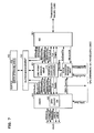
- FIG. 7 A detailed connection between the SIE 30, the end point management circuit 40, the buffer management circuit 50, the buffer 60, the bulk transfer management circuit 70, and the DMAC 80 is shown in Fig. 7.
- SIEReadData is data (IN data) to be read from the buffer 60 (the data storage area 62) and transferred to the host through USB (the first bus).
- SIEWriteData is data (OUT data) to be transferred from the host by USB and written to the buffer 60.
- DMAReadData is data to be read from the buffer 60 and transferred (by DMA transfer) to a device such as a hard disk drive HDD through EBUS (the second bus).
- DMAWriteData is data to be transferred from the HDD or the like through EBUS and written to the buffer 60.
- a SIEReadReq signal that is output from the SIE 30 is a signal that requests the reading of SIEReadData
- SIEReadAck that is output from the end point management circuit 40 is an acknowledge signal with respect to SIEReadReq.
- SIEWriteReq is a signal that requests the writing of SIEWriteData
- SIEWriteAck is an acknowledge signal with respect to SIEWriteReq.
- the DMAReadReq signal that is output from the DMAC 80 is a signal for requesting the reading of DMAReadData
- DMAReadAck that is output from the end point management circuit 40 is an acknowledge signal with respect to DMAReadReq.
- DMAWriteReq is a signal that requests the writing of DMAWriteData
- DMAWriteAck is an acknowledge signal with respect to DMAWriteReq.
- the Full signal indicates whether or not the data storage area 62 of the buffer 60 is full, and the Empty signal indicates whether or not the data storage area 62 is empty.
- the determination of whether or not the data storage area 62 is full, or whether or not it is empty, is based on a count from a residual data size counter 41 that counts the size of data remaining in the data storage area 62 (residual data area).
- the data storage area 62 of this embodiment is an area in which data that is input first thereto is output first therefrom (FIFO: an area set to FIFO).
- the data storage area 62 can be set to be a first-in, first-out area by configuring it of serially connected registers or memory, or it could be set to be a first-in, first-out area by skillful address control of RAM.
- a HaveMPS signal that is output by the end point management circuit 40 indicates whether or not the size of data (data length) remaining in the data storage area 62 of the buffer 60 is the maximum packet size. Taking the maximum packet size to be 512 bytes by way of example, HaveMPS is active (high) when the residual data size is 512 bytes (or more) and HaveMPS goes inactive (low) when the residual data size is between 0 to 511 bytes. In this case, the residual data size is obtained by the residual data size counter 41.
- An HDDATA signal is data to be transferred by DMA through EBUS (the second bus), xDMACK is an acknowledgment signal with respect to that DMA transfer, and xDMARQ is a request signal for DMA transfer.
- xHIOR is a read pulse signal and xHIOW is a write pulse signal.
- the CPU uses a DMA_Start signal to indicate the start of DMA transfer.
- a DMA_Running signal indicates that DMA transfer through EBUS is in progress; it goes active (high) at the beginning of DMA transfer by EBUS and inactive (low) at the end of the DMA transfer. In other words, DMA_Running is active during the period of data transfer (data phase) by EBUS.
- An AutoEnShort signal is used to set the automatic transmission of a short packet that exists within the data storage area 62 of the buffer 60 to either enabled or disabled.
- An EnShortPkt signal indicates the transfer of a short packet to the SIE 30.
- EnShortPkt becomes active. This causes the automatic transmission through USB of the short packet (a packet of less than the maximum packet size) that exists in the data storage area 62, by the SIE 30.
- An INTranACK signal is an acknowledgment of the IN transaction; it goes active when the host replies appropriately.
- a BulkDMACmp signal indicates that the data phase (transfer of all the data) has ended, during bulk transfer.
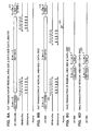
- a timing waveform chart shown in Fig. 8A illustrates a case in which the size of the remaining area (empty area) of the data storage area 62 (FIFO) of the buffer 60 is greater than or equal to the size of data (data length) that is being transferred from the host, during an OUT transaction (data transfer in a first direction, for transferring data from the host to the device).
- an ACK can be returned to the host, as shown at C1 in Fig. 8A.
- the data storage area 62 has a single-buffer structure instead of a double-buffer structure, it will not be possible to receive the next packet from the host when in HS mode, until the data storage area 62 is emptied. In such a case, therefore, NYET is returned to the host instead of ACK. Even with a double-buffer structure, it could happen that the next data cannot be received because both buffers are in use, in which case NYET is returned to the host instead of ACK, in a similar manner.
- a timing waveform chart shown in Fig. 8B illustrates a case in which the data size is less than the size of the remaining area of the data storage area 62, during an OUT transaction.
- a Rewind signal becomes active as shown at C3.
- the buffer management circuit 50 when the SIE 30 makes SIEWriteReq active at C4 and C5 in Figs. 8A and 8B, the buffer management circuit 50 generates the write address for SIEWriteData in accordance with the instruction from the end point management circuit 40, and outputs it to the buffer 60.
- SIEWriteData (of four bytes, by way of example) to be written into the data storage area 62 of the buffer 60 and SIEWriteAck to be returned to the SIE 30.
- the data from the host (such as 512 bytes of data) is written sequentially into the data storage area 62 by repeating this write processing four bytes at a time.
- Timing waveform charts shown in Figs. 8C and 8D illustrate the PING transaction (PING protocol) by which the host enquires from the device whether or not the data storage area 62 is empty.
- PING transaction PING protocol
- This PING transaction is supported in USB HS mode. This protocol is used when NYET has been received from the device with respect to an OUT token or OUT data from the host.
- a timing waveform chart shown in Fig. 9A illustrates a case in which the size of data (valid data) remaining in the data storage area 62 is greater than or equal to the maximum packet size during an IN transaction (data transfer in a second direction, for transferring data from the device to the host) .
- ACK is returned from the host to the device when data of the maximum packet size has been transferred to the host, as shown at D1 in Fig. 9A.
- the buffer management circuit 50 when the SIE 30 makes SIEReadReq active at D2 in Fig. 9A, the buffer management circuit 50 generates the read address for SIEReadData in accordance with the instruction from the end point management circuit 40, and outputs it to the buffer 60.
- SIEReadData (of four bytes, by way of example) to be written into the data storage area 62 of the buffer 60 and SIEReadAck to be returned to the SIE 30.
- the data to be transferred to the host is read sequentially into the data storage area 62 by repeating this read processing four bytes at a time.
- a timing waveform chart shown in Fig. 9B illustrates a case in which the size of data remaining in the data storage area 62 is less than the maximum packet size, and also EnShortPkt (see Fig. 7) is low (inactive). In this case, the transfer of a short packet (a packet of less than the maximum packet size) is inhibited by EnShortPkt being low, as shown at D3, D4, and D5 in Fig. 9B. NAK is therefore returned in answer to IN tokens from the host, as shown at D6, D7, and D8.
- a timing waveform chart shown in Fig. 9C illustrates a case in which the size of data remaining in the data storage area 62 is less than the maximum packet size, and also EnShortPkt is high (active). In this case, the transfer of a short packet is permitted because EnShortPkt is high, as shown at D9 in Fig. 9C, and a short packet that exists in the data storage area 62 is transferred as appropriate to the host, as shown at D10.
- the data storage area 62 of the buffer 60 could be an area used in common for OUT transactions and IN transactions, or it could be separate areas.
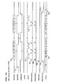
- a timing waveform chart shown in Fig. 10 relates to DMA transfer during data transmission to a device such as a hard disk drive HDD.
- DMAReadReq and DMAReadAck are then used for handshaking, as shown at E4 and E5, and a quantity of data, such as four bytes (32 bits) is read from the data storage area 62 of the buffer 60.
- the thus-read four bytes of data are transmitted to the HDD two bytes at a time, by way of example, through the 16-bit bus EBUS, using the write pulse signal xHIOW, as shown at E6 and E7.
- the value Count (number of data transfers) in the DMA counter 82 is decremented, as shown at E8. Note that the setting of the initial value N of Count is based on dCBWDTransferLength of the CBW of Fig. 3.
- DMA_Running becomes inactive, as shown at E10.
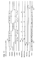
- a timing waveform chart shown in Fig. 11 relates to DMA transfer during data reception from a device such as a hard disk drive HDD.
- Data from the HDD is then received through EBUS, using read pulse signal xHIOR, as shown at F4 and F5.
- the thus-received data is written to data storage area 62 of the buffer 60 by handshaking using DMAWriteReq and DMAWriteAck, as shown at F6 and F7.
- the IN token (the token at B4 in Fig. 5B) transferred from the host will be recognized erroneously as an IN token with respect to the CSW (B6), which could cause a data transfer error.
- a CBW (command) and OUT data are allocated as information to be transferred through the bulk-out end point EP1
- CSW (status) and IN data are allocated as information to be transferred through the bulk-in end point EP2.
- the host and device must therefore distinguish which type of information is to be transferred through each of the end points.
- the host and the device determine what phase is the current phase and also distinguish this information.
- the current phase is the command phase at B1 and B2 of Figs. 5A and 5B, by way of example, it is determined that the information to be transferred through the end point EP1 is a CBW. Since the current phase is the data phase at B3 and B4, it is determined that the information to be transferred through the end point EP1 is OUT data and the information to be transferred through the end point EP2 is IN data. Furthermore, since the current phase is the status phase at B5 and B6, it is determined that the information to be transferred through the end point EP2 is a CSW.
- the determination of the switch from the data phase to the status phase is implemented by the method described below.
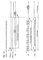
- the end of the data phase (the end of all data transfer and the switching of phases) is determined as shown in Fig. 12.
- the data transfer (data phase) through USB starts as shown at G1 in Fig. 12.
- the Empty signal that indicates whether or not the data storage area 62 is empty becomes inactive as shown at G2, to indicate that the data storage area 62 is not empty.
- the CPU then makes DMA_Running go active by setting DMA_Start to active, as shown at G3 and G4, and data transfer (EBUS data phase) through EBUS (the second bus) starts.
- the timing of G6 is delayed until after the timing of G5, which ends the USB data transfer. This G6 timing also matches the timing at G7 at which the Empty signal goes active because the data storage area 62 of the buffer 60 is empty.
- the timing of G6 is determined by using the DMA counter 82 of Fig. 12, which is provided on the EBUS side, to count the data size (number of transfers and data length) (see E9 in Fig. 10).
- the end of the data phase is determined by the condition that data transmission through EBUS (second bus) has ended during an OUT transaction (data transfer in the first direction).
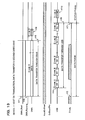
- DMA_Running goes active and the data transfer through EBUS starts when the CPU sets DMA_Start to active, as shown at H1 and H2. If the data that has been transferred through EBUS is written into the data storage area 62 of the buffer 60, Empty becomes inactive as shown at H3, to indicate that the data storage area 62 is not empty.
- Data transfer by USB then starts, as shown at H4.
- the data to be transferred by USB is read from the data storage area 62, and Empty becomes active if the data storage area 62 becomes empty.
- the timing of H6 can be determined by using the DMA counter 82 provided on the EBUS side to count the size of data transferred by EBUS.
- the timing of H7 matches the timing of H8 at the end of data transfer (data phase) through USB (the first bus).
- the end of the data phase during an IN transaction is determined on condition that data reception through the EBUS (second bus) has ended and also the data storage area of the buffer 60 has become empty.
- the end of the data phase during an OUT transaction is determined on condition that the count of the counter on the EBUS side has reached 0, whereas the end of the data phase during an IN transaction is determined on condition that the count of the counter on the USB side has reached 0, by way of example.
- the method of this embodiment shown in Figs. 12 and 13 need only provide a counter on the EBUS (second bus) side, as shown in Fig. 7, making it unnecessary to provide a counter on the USB (first bus) side. It is therefore possible to simplify the circuit control and also simplify the circuit configuration, making the data transfer control device more compact and inexpensive.
- the firmware processing for controlling the data transfer control device can also be simplified, enabling an increase in the effective data transfer speed.
- the thus-generated CSW is transmitted to the host side through USB (the first bus) in the status phase after the end of the data phase, as shown at H10 in Fig. 13.
- a short packet has a special meaning as a payload size that is less than the maximum packet size.
- the host determines that is the end of the data phase and moves on to the status phase.
- the device therefore controls data transfer to ensure that no short packet is sent to the host, except when the data phase is to end.
- the device always checks the size of data remaining in the data storage area 62 of the buffer 60. If the residual data size is greater than or equal to maximum packet size, a data packet of the maximum packet size is created from the residual data, for transfer to the host. If it is determined that the residual data size is less than the maximum packet size, it permits the transfer of a short packet and sends a packet of that residual data size as a short packet to the host. This enables the end of the data phase.
- this embodiment utilizes a method whereby a short packet in the data storage area 62 is transmitted automatically (by hardware processing, not by firmware processing) through the USB (first bus) , if data reception (DMA transfer) through EBUS (the second bus) has ended and also the size of data remaining in the data storage area 62 (valid data) is less than the maximum packet size.
- a timing waveform chart shown in Fig. 14 illustrates a case in which the size of data remaining in the data storage area 62 is less than the maximum packet size during an IN transaction (data transfer in the second direction), by way of example.
- an AutoEnShort signal (see Fig. 7) which sets the automatic transmission of a short packet (automatic transfer) to either enabled or disabled is set to be active (high), as shown at I1.
- the level of AutoEnShort is set by the firmware (CPU) writing a given value to an AutoEnShort register during enumeration. In this case, AutoEnShort could be set to be always active for a device in which the automatic transmission of short packet would always be valid, such as a mass storage device.
- EnShortPkt goes active as shown at 14 to indicate to the SIE 30 the automatic transmission of s short packet.
- EnShortPkt goes active when AutoEnShort is active and HaveMPS, which indicates whether or not the residual data size is the maximum packet size, is inactive.
- a short packet in the data storage area 62 can be transmitted automatically by the hardware by setting AutoEnShort to active. It is therefore not necessary for the firmware to perform processing to check the size of data remaining in the data storage area 62. As a result, the processing load on the firmware can be reduced, enabling an increase in the effective data transfer speed.
- the method of this embodiment shown in Fig. 14 makes it possible to change to the status phase at an earlier stage, since the process of checking the residual data size is not performed by the firmware. As a result, the effective data transfer speed can be increased far more than in the case in which the process of checking the residual data size is performed by the firmware.
- AutoEnShort is set to active. This makes it possible to transmit a short packet automatically and change to the status phase, without firmware processing.
- the data transfer control device therefore attaches control information (header and footer) comprising data size after data has been received from the scanner, for transfer to the host. For that reason, the size of data transferred through EBUS does not match the size of data transferred through USB, so it is not possible to permit unconditionally transfer of a short packet to the host, and thus it is necessary to set AutoEnShort to inactive.
- This embodiment therefore makes it possible to adjust flexibly to data transfer in devices such as scanners in addition to mass storage devices such as hard disk drives, by freely setting the automatic transmission of a short packet to enabled or disabled.
- the AutoEnShort signal shown in Fig. 14 is used for automatic transmission of a short packet in the data storage area 62.
- the CPU could be notified of the presence of a short packet in the data storage area 62.
- the configuration is such that an interrupt is used to notify the CPU (processing unit) of the presence of a short packet in the data storage area 62, if data reception through EBUS (the second bus) ends and also the size of data remaining in the data storage area 62 is less than the maximum packet size.
- FIG. 15 A detailed example of connections between the SIE 30, the end point management circuit 40, the buffer management circuit 50, the buffer 60, the bulk transfer management circuit 70, and the DMAC 80 when such a method is used is shown in Fig. 15.
- Fig. 15 differs from the previously described Fig. 7 in that the bulk transfer management circuit 70 outputs an interrupt signal ShortINT to the CPU (a register that can be accessed by the CPU) and EnShortPkt is set by the CPU and input to the SIE 30.
- ShortINT a register that can be accessed by the CPU
- EnShortPkt is set by the CPU and input to the SIE 30.
- ShortINT is an interrupt signal for notifying the CPU of the presence of a short packet in the data storage area 62
- EnShortPkt is a signal that indicates to the SIE 30 the transfer of the short packet by the CPU.
- ShortINT becomes active to notify the CPU of the presence in the data storage area 62 of a short packet that can be transferred.
- the CPU performs determination processing for transferring the short packet and, if it is determined that a short packet can be transferred, it sets EnShortPkt to active. This causes the SIE 30 to read the short packet that is in the data storage area 62 and perform processing to transfer it through USB to the host.
- a timing waveform chart of Fig. 16 shows the operation during an IN transaction (data transfer in the second direction) when size of data remaining in the data storage area 62 is less than the maximum packet size.
- ShortINT goes active to inform the CPU of the presence of the short packet, as shown at J4.
- ShortINT goes active when DMA_Running is inactive and HaveMPS, which indicates whether or not the residual data size is the maximum packet size, is inactive.
- the CPU firmware
- this ShortINT performs processing to attach information such as data size to the received data (processing to write the attached information to the data storage area 62).
- EnShortPkt then goes active, as shown at J5. This causes the transfer of the data in the data storage area 62 to the host by the SIE 30, as shown at J6.
- the data phase then ends and the status phase starts, as shown at J7.
- ShortINT is used to notify the firmware operating on the CPU of the presence of the short packet in the data storage area 62. This makes it possible to implement suitable data transfer, even in a device such as a scanner, in which information such as data size is finally added to received data.
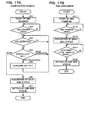
- FIG. 17A A flowchart of the processing performed by the firmware of a comparative example during an IN transaction is shown in Fig. 17A.
- Fig. 17B A flowchart of the processing performed by the firmware in accordance with the method of this embodiment, which automatically transmits a short packet, is shown in Fig. 17B.
- the firmware first sets DMA_Start to 1 (high), to cause the start of DMA transfer through the EBUS (step S1). It then checks DMA_Running to determine whether or not DMA transfer through the EBUS has ended (step S2).
- the firmware uses IntranACK to detect ACK from the USB side (step S3). If ACK has been detected, the firmware checks the residual data size RDS in the data storage area of the buffer (step S4). If RDS is greater than or equal to the maximum packet size MaxPacketSize, the flow returns to step S3 to wait for the arrival of the next ACK.
- EnShortPkt is set to 1 (step S5). This causes the transfer of a short packet from the data storage area to the host. The flow then returns to step S3, to wait for the next ACK.
- step S6 If RDS is 0, it is considered that all of the data in the data storage area has been transferred, so the firmware acquires the EBUS-side status (step S6).
- the firmware generates the CSW on the basis of the thus-acquired status, and sets the status to be sent to the USB side (step S7).
- the firmware first sets DMA_Start to 1, to cause the start of DMA transfer through the EBUS (step S11). Note that AutoEnShort is set to 1 before the DMA transfer. The firmware checks DMA_Running to determine whether or not DMA transfer through the EBUS has ended (step S12).
- the firmware acquires the EBUS-side status (step S13).
- the firmware determines whether or not the data phase (transfer of all the data) has ended (step S14). In other words, it determines whether or not the data storage area of the buffer area has become empty and the ACK referring to the final packet has been returned from the host. If it has been determined that the data phase has ended, the firmware generates the CSW on the basis of the status acquired in step S13, and sets the status to be sent to the USB side (step S15).
- step S4 the processing for checking the residual data size (step S4) that is necessary with the comparative example of Fig. 17A is not necessary with the embodiment of Fig. 17B.
- the processing for setting EnShortPkt to active is also done by hardware, so there's no need to have the firmware do it. It is therefore possible to reduce the processing load on the firmware, thus increasing the effective data transfer speed.
- FIG. 18 A flowchart shown in Fig. 18 is of the processing performed by the firmware in the method of using an interrupt to notify the firmware of the presence of a short packet (Figs. 15 and 16).
- the firmware first causes the start of DMA transfer by EBUS, then it determines whether or not DMA transfer has ended (steps S21 and S22).
- the firmware determines whether or not the interrupt signal ShortINT has been detected (at J4 in Fig. 16) (step S23). If ShortINT has been detected, the firmware writes to the data storage area (FIFO) the information that is to be attached to the receive data of the DMA transfer (such as the data size) (step S24).
- step S25 If it is determined that all of the information has been attached (step S25), the firmware sets EnShortPkt to 1 (step S26).
- step S27 It then detects ACK from the USB side (step S27). If ACK has been detected, the firmware checks whether or not the residual data size RDS in the data storage area is 0 (step S28). If RDS is not 0, the flow returns to step S27 and the firmware waits for the next ACK to be detected.
- step S29 If RDS is 0, on the other hand, it is considered that all of the data in the data storage area has been transferred, so the firmware acquires the EBUS-side status (step S29). The firmware generates the CSW on the basis of the thus-acquired status, and sets the status to be sent to the USB side (step S30).
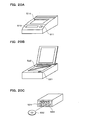
- FIG. 19A An internal block diagram of a printer that is one example of such electronic equipment is shown in Fig. 19A with an external view thereof being shown in Fig. 20A.
- a CPU (microcomputer) 510 has various functions, including that of controlling the entire system.
- An operating section 511 is designed to enable the user to operate the printer.
- Data such as a control program and fonts is stored in a ROM 516, and a RAM 517 functions as a work area for the CPU 510.
- a DMAC 518 is a DMA controller for transferring data through the CPU 510.
- a display panel 519 is designed to inform the user of the operational state of the printer.
- Serial print data that has been send in from another device such as a personal computer via USB is converted into parallel print data by a data transfer control device 500.
- the thus converted parallel print data is sent to a print processing section (a printer engine) 512 by the CPU 510 or the DMAC 518.
- This parallel print data is subjected to given processing in the print processing section 512 and is output for printing to paper by a print section (a device for outputting data) 514 comprising components such as a print head.
- FIG. 19B An internal block diagram of a scanner that is another example of electronic equipment is shown in Fig. 19B with an external view thereof being shown in Fig. 20B.
- a CPU 520 has various functions, including that of controlling the entire system.
- An operating section 521 is designed to enable the user to operate the scanner.
- Data such as a control program is stored in a ROM 526, and a RAM 527 functions as a work area for the CPU 520.
- a DMAC 528 is a DMA controller.
- An image of a document is read in by an image read section (a device for fetching data) 522, which comprises components such as a light source and an opto-electric converter, and data of the read-in image is processed by an image processing section (a scanner engine) 524.
- the processed image data is sent to the data transfer control device 500 by the CPU 520 or DMAC 528.
- the data transfer control device 500 converts that parallel image data into serial data and sends it to another device such as a personal computer via USB.
- FIG. 19C An internal block diagram of a CD-RW drive that is a further example of electronic equipment is shown in Fig. 19C with an external view thereof being shown in Fig. 20C.
- a CPU 530 has various functions, including that of controlling the entire system.
- An operating section 531 is designed to enable the user to operate the CD-RW drive.
- Data such as a control program is stored in a ROM 536, and a RAM 537 functions as a work area for the CPU 530.
- a DMAC 538 is a DMA controller.
- the data that has been subjected to this signal processing is sent to the data transfer control device 500 by the CPU 530 or the DMAC 538.
- the data transfer control device 500 converts this parallel data into serial data, then sends it to another device such as a personal computer via USB.
- Serial data that comes in from another device via USB is converted into parallel data by the data transfer control device 500.
- This parallel data is sent to the signal processing section 534 by the CPU 530 or the DMAC 538.
- This parallel print data is subjected to given signal processing by the signal processing section 534 then is stored by the read/write section 533 on the CD-RW 532.
- a separate CPU for controlling data transfer by the data transfer control device 500 could be provided in addition to the CPU 510, 520, or 530 of Fig. 19A, Fig. 19B, Fig. 19C.
- the electronic equipment that can employ a data transfer control device in accordance with the present invention is not limited to the above described embodiment, and thus various other examples can be considered, such as various types of optical disk drive (CD-ROM or DVD), magneto-optical (MO) disk drives, hard disk drives, TVs, VCRs, video cameras, audio equipment, telephones, projectors, personal computers, electronic organizers, and dedicated wordprocessors.
- CD-ROM or DVD compact disc-read only memory
- MO magneto-optical
- the configuration of the data transfer control device in accordance with the present invention is not limited to that shown in Figs. 6, 7, and 15, and thus various modifications thereof are possible.
- the present invention can also be applied to data transfer in accordance with a standard that is based on a concept similar to that of USB 2.0, or a standard that is developed from USB 2.0.
Landscapes
- Engineering & Computer Science (AREA)
- Theoretical Computer Science (AREA)
- General Engineering & Computer Science (AREA)
- Physics & Mathematics (AREA)
- General Physics & Mathematics (AREA)
- Computer Hardware Design (AREA)
- Information Transfer Systems (AREA)
- Bus Control (AREA)
- Selective Calling Equipment (AREA)
- Communication Control (AREA)
- Small-Scale Networks (AREA)
Abstract
Description
wherein the end of a data phase for the transfer of data during the data transfer in the second direction is determined on condition that data reception through the second bus has ended and also the data storage area of the buffer has become empty.
Claims (15)
- A data transfer control device for data transfer through a bus, comprising:wherein the end of a data phase for the transfer of data during the data transfer in the first direction is determined on condition that data transmission through the second bus has ended; anda buffer having a data storage area for storing data that is received through a first bus and transmitted through a second bus during data transfer in a first direction, and for storing data that is received through the second bus and transmitted through the first bus during data transfer in a second direction; anda buffer management circuit which manages the writing of data into the data storage area of the buffer and the reading of data from the data storage area,
wherein the end of a data phase for the transfer of data during the data transfer in the second direction is determined on condition that data reception through the second bus has ended and also the data storage area of the buffer has become empty. - The data transfer control device as defined in claim 1; further comprising:a counter which counts the size of data transmitted or received through the second bus.
- The data transfer control device as defined in claim 1 or 2,
wherein the status of the data reception through the second bus is acquired; and
wherein the thus-acquired status is transmitted though the first bus during a status phase after the end of the data phase. - The data transfer control device as defined in any one of claims 1 to 3,
wherein a short packet in the data storage area is automatically transmitted through the first bus, when data reception through the second bus ends and also the size of data remaining in the data storage area of the buffer is less than the maximum packet size. - The data transfer control device as defined in any one of claims 1 to 4,
wherein a processing unit is notified of the presence of a short packet in the data storage area, when data reception through the second bus ends and also the size of data remaining in the data storage area of the buffer is less than the maximum packet size. - A data transfer control device for data transfer through a bus, comprising:wherein a short packet in the data storage area is automatically transmitted through the first bus, when data reception through the second bus ends and also the size of data remaining in the data storage area of the buffer is less than the maximum packet size.a buffer having a data storage area for storing data that is received through a second bus and transmitted through a first bus; anda buffer management circuit which manages the writing of data into the data storage area of the buffer and the reading of data from the data storage area,
- The data transfer control device as defined in claim 4 or 6, further comprising:a unit which sets the automatic transmission of a short packet from the data storage area to either enabled or disabled.
- The data transfer control device as defined in claim 7,
wherein the automatic transmission is set to be disabled when data that has been received through the second bus has given information and is transmitted through the first bus. - A data transfer control device for data transfer through a bus, comprising:wherein a processing unit is notified of the presence of a short packet in the data storage area, when data reception through the second bus ends and also the size of data remaining in the data storage area of the buffer is less than the maximum packet size.a buffer having a data storage area for storing data that is received through a second bus and transmitted through a first bus; anda buffer management circuit which manages the writing of data into the data storage area of the buffer and the reading of data from the data storage area,
- The data transfer control device as defined in any one of claims 1 to 9,
wherein information that has been input first to the data storage area is output first from the data storage area. - The data transfer control device as defined in any one of claims 1 to 10,
wherein data transfer is in accordance with the universal serial bus (USB) standard. - Electronic equipment comprising:the data transfer control device as defined in any one of claims 1 to 11; anda device which performs output processing, fetch processing, or storage processing on data transferred through the data transfer control device and the bus.
- A data transfer control method for data transfer through a bus, comprising:providing a data storage area on a buffer for storing data that is received through a first bus and transmitted through a second bus during data transfer in a first direction, and for storing data that is received through a second bus and transmitted through a first bus during data transfer in a second direction;managing the writing of data into the data storage area of the buffer and the reading of data from the data storage area;determining the end of a data phase for the transfer of data during the data transfer in the first direction on condition that data transmission through the second bus has ended; anddetermining the end of a data phase for the transfer of data during the data transfer in the second direction on condition that data reception through the second bus has ended and also the data storage area of the buffer has become empty.
- A data transfer control method for data transfer through a bus, comprising:providing a data storage area on a buffer for storing data that is received through a second bus and transmitted through a first bus;managing the writing of data into the data storage area of the buffer and the reading of data from the data storage area; andautomatically transmitting a short packet in the data storage area through the first bus, when data reception through the second bus ends and also the size of data remaining in the data storage area of the buffer is less than the maximum packet size.
- A data transfer control method for data transfer through a bus, comprising:providing a data storage area on a buffer for storing data that is received through a second bus and transmitted through a first bus;managing the writing of data into the data storage area of the buffer and the reading of data from the data storage area; andcausing a processing unit to be notified of the presence of a short packet in the data storage area, when data reception through the second bus ends and also the size of data remaining in the data storage area of the buffer is less than the maximum packet size.
Applications Claiming Priority (2)
| Application Number | Priority Date | Filing Date | Title |
|---|---|---|---|
| JP2001143431A JP3870717B2 (en) | 2001-05-14 | 2001-05-14 | Data transfer control device and electronic device |
| JP2001143431 | 2001-05-14 |
Publications (3)
| Publication Number | Publication Date |
|---|---|
| EP1260908A2 true EP1260908A2 (en) | 2002-11-27 |
| EP1260908A3 EP1260908A3 (en) | 2003-05-14 |
| EP1260908B1 EP1260908B1 (en) | 2005-08-03 |
Family
ID=18989584
Family Applications (1)
| Application Number | Title | Priority Date | Filing Date |
|---|---|---|---|
| EP02010402A Expired - Lifetime EP1260908B1 (en) | 2001-05-14 | 2002-05-08 | Data transfer control device, electronic equipment, and data transfer control method |
Country Status (8)
| Country | Link |
|---|---|
| US (1) | US6901465B2 (en) |
| EP (1) | EP1260908B1 (en) |
| JP (1) | JP3870717B2 (en) |
| KR (1) | KR100460650B1 (en) |
| CN (1) | CN1282094C (en) |
| AT (1) | ATE301307T1 (en) |
| DE (1) | DE60205305T2 (en) |
| TW (1) | TW556090B (en) |
Cited By (1)
| Publication number | Priority date | Publication date | Assignee | Title |
|---|---|---|---|---|
| WO2008017872A1 (en) | 2006-08-11 | 2008-02-14 | Aspex Semiconductor Limited | Improvements relating to direct data input/output interfaces |
Families Citing this family (26)
| Publication number | Priority date | Publication date | Assignee | Title |
|---|---|---|---|---|
| US7386003B1 (en) * | 2000-03-27 | 2008-06-10 | Bbn Technologies Corp. | Systems and methods for communicating in a personal area network |
| US6804232B1 (en) * | 2000-03-27 | 2004-10-12 | Bbnt Solutions Llc | Personal area network with automatic attachment and detachment |
| JP3680763B2 (en) * | 2001-05-14 | 2005-08-10 | セイコーエプソン株式会社 | Data transfer control device and electronic device |
| US7421257B1 (en) | 2001-11-30 | 2008-09-02 | Stragent, Llc | Receiver scheduling in ad hoc wireless networks |
| JP3703439B2 (en) * | 2002-03-19 | 2005-10-05 | Necマイクロシステム株式会社 | Data transfer control device and method |
| JP2004029898A (en) * | 2002-06-21 | 2004-01-29 | Renesas Technology Corp | Data processor |
| JP2005100064A (en) * | 2003-09-24 | 2005-04-14 | Canon Inc | Image processing apparatus, image processing method, and program |
| JP2005122372A (en) | 2003-10-15 | 2005-05-12 | Seiko Epson Corp | Data transfer control device, electronic device, and data transfer control method |
| US20080301358A1 (en) * | 2004-05-25 | 2008-12-04 | Chih-Chiang Wen | Electronic device that Downloads Operational Firmware from an External Host |
| US20050268029A1 (en) * | 2004-05-25 | 2005-12-01 | Chih-Chiang Wen | Optical Disc Drive that Downloads Operational Firmware from an External Host |
| US20050265266A1 (en) * | 2004-05-25 | 2005-12-01 | Chih-Chiang Wen | Optical disc drive that downloads operational firmware from an external host |
| US20050273541A1 (en) * | 2004-06-04 | 2005-12-08 | Texas Instruments Incorporated | Circuit and method for adaptively recognizing a data packet in a universal serial bus network device |
| WO2005125093A2 (en) * | 2004-06-15 | 2005-12-29 | Koninklijke Philips Electronics N.V. | Bus controller for handling split transactions |
| JP4567433B2 (en) * | 2004-12-27 | 2010-10-20 | ルネサスエレクトロニクス株式会社 | Host apparatus, device apparatus, communication system, and data transmission / reception method |
| JP2006215873A (en) * | 2005-02-04 | 2006-08-17 | Toshiba Corp | Control apparatus, information processing apparatus, and transfer processing method |
| JP4412191B2 (en) * | 2005-02-04 | 2010-02-10 | セイコーエプソン株式会社 | Data transfer control device and electronic device |
| JP2006235994A (en) | 2005-02-24 | 2006-09-07 | Nec Electronics Corp | Bridge system, bridge system control method, information processing apparatus, peripheral equipment, and program |
| US7640378B2 (en) * | 2005-03-11 | 2009-12-29 | Icron Technologies Corporation | Method and apparatus for improving the performance of USB mass storage devices in the presence of long transmission delays |
| JP4966505B2 (en) * | 2005-03-24 | 2012-07-04 | ブラザー工業株式会社 | Packet communication system |
| JP4931912B2 (en) * | 2006-04-26 | 2012-05-16 | パナソニック株式会社 | Signal transmission method, transmission / reception apparatus, and communication system |
| JP4337891B2 (en) * | 2007-03-01 | 2009-09-30 | セイコーエプソン株式会社 | Storage terminal and information processing system |
| US20090083475A1 (en) * | 2007-09-24 | 2009-03-26 | Mediatek Inc. | Apparatus and method for updating firmware stored in a memory |
| CN101458672B (en) * | 2007-12-10 | 2011-08-24 | 联想(北京)有限公司 | Hot plug equipment, computer and data-transmission indicating method |
| TW200945052A (en) * | 2008-04-21 | 2009-11-01 | Ralink Technology Corp | Method for increasing USB transmission rate |
| US20160357462A1 (en) * | 2015-06-08 | 2016-12-08 | Samsung Electronics Co., Ltd. | Nonvolatile Memory Modules and Data Management Methods Thereof |
| TWI812490B (en) * | 2022-09-27 | 2023-08-11 | 宏達國際電子股份有限公司 | Signal transceiving device and signal transceiving method thereof |
Family Cites Families (31)
| Publication number | Priority date | Publication date | Assignee | Title |
|---|---|---|---|---|
| US5131081A (en) * | 1989-03-23 | 1992-07-14 | North American Philips Corp., Signetics Div. | System having a host independent input/output processor for controlling data transfer between a memory and a plurality of i/o controllers |
| JP3515142B2 (en) * | 1992-06-11 | 2004-04-05 | セイコーエプソン株式会社 | Data transfer control device |
| US5546546A (en) * | 1994-05-20 | 1996-08-13 | Intel Corporation | Method and apparatus for maintaining transaction ordering and arbitrating in a bus bridge |
| US5771359A (en) * | 1995-10-13 | 1998-06-23 | Compaq Computer Corporation | Bridge having a data buffer for each bus master |
| JP2996179B2 (en) * | 1996-07-22 | 1999-12-27 | 日本電気株式会社 | PCI bus system |
| US6185641B1 (en) * | 1997-05-01 | 2001-02-06 | Standard Microsystems Corp. | Dynamically allocating space in RAM shared between multiple USB endpoints and USB host |
| US5987554A (en) * | 1997-05-13 | 1999-11-16 | Micron Electronics, Inc. | Method of controlling the transfer of information across an interface between two buses |
| US6073190A (en) * | 1997-07-18 | 2000-06-06 | Micron Electronics, Inc. | System for dynamic buffer allocation comprising control logic for controlling a first address buffer and a first data buffer as a matched pair |
| US6128673A (en) | 1997-11-14 | 2000-10-03 | Aronson; Michael D. | Method and apparatus for communication and translation of a plurality of digital protocols |
| US6279087B1 (en) * | 1997-12-22 | 2001-08-21 | Compaq Computer Corporation | System and method for maintaining coherency and improving performance in a bus bridge supporting write posting operations |
| KR100290729B1 (en) | 1998-01-07 | 2001-05-15 | 클라크 3세 존 엠. | Apparatus and method of transmitting and receiving usb isochronous data |
| US6154465A (en) * | 1998-10-06 | 2000-11-28 | Vertical Networks, Inc. | Systems and methods for multiple mode voice and data communications using intelligenty bridged TDM and packet buses and methods for performing telephony and data functions using the same |
| JP3231017B2 (en) * | 1998-05-25 | 2001-11-19 | 日本電信電話株式会社 | Packet network transfer method |
| US6266715B1 (en) | 1998-06-01 | 2001-07-24 | Advanced Micro Devices, Inc. | Universal serial bus controller with a direct memory access mode |
| US6628653B1 (en) * | 1998-06-04 | 2003-09-30 | Nortel Networks Limited | Programmable packet switching device |
| US6161160A (en) * | 1998-09-03 | 2000-12-12 | Advanced Micro Devices, Inc. | Network interface device architecture for storing transmit and receive data in a random access buffer memory across independent clock domains |
| US6202101B1 (en) * | 1998-09-30 | 2001-03-13 | Compaq Computer Corporation | System and method for concurrently requesting input/output and memory address space while maintaining order of data sent and returned therefrom |
| JP3543648B2 (en) * | 1998-10-27 | 2004-07-14 | セイコーエプソン株式会社 | Data transfer control device and electronic equipment |
| JP3543647B2 (en) * | 1998-10-27 | 2004-07-14 | セイコーエプソン株式会社 | Data transfer control device and electronic equipment |
| US6289406B1 (en) * | 1998-11-06 | 2001-09-11 | Vlsi Technology, Inc. | Optimizing the performance of asynchronous bus bridges with dynamic transactions |
| US6219737B1 (en) * | 1998-12-10 | 2001-04-17 | International Business Machines Corporation | Read request performance of a multiple set buffer pool bus bridge |
| US6405276B1 (en) * | 1998-12-10 | 2002-06-11 | International Business Machines Corporation | Selectively flushing buffered transactions in a bus bridge |
| US6256699B1 (en) * | 1998-12-15 | 2001-07-03 | Cisco Technology, Inc. | Reliable interrupt reception over buffered bus |
| TW413763B (en) * | 1999-03-16 | 2000-12-01 | Winbond Electronics Corp | Data conversion device and data flow control method in between USB host and network end |
| US6460108B1 (en) * | 1999-03-31 | 2002-10-01 | Intel Corporation | Low cost data streaming mechanism |
| JP2001036546A (en) * | 1999-07-16 | 2001-02-09 | Hitachi Ltd | Receive buffer control device |
| US6708244B2 (en) * | 1999-07-22 | 2004-03-16 | Cypress Semiconductor Corp. | Optimized I2O messaging unit |
| US6711181B1 (en) * | 1999-11-17 | 2004-03-23 | Sony Corporation | System and method for packet parsing and data reconstruction in an IEEE 1394-1995 serial bus network |
| US6684272B1 (en) * | 1999-12-23 | 2004-01-27 | Intel Corporation | Throughput enhancement for a universal host controller interface in a universal serial bus |
| US6529521B1 (en) * | 1999-12-27 | 2003-03-04 | Emc Corporation | Data storage system |
| US6807585B2 (en) * | 2001-02-22 | 2004-10-19 | Ati Technologies, Inc. | Method and system for parsing section data |
-
2001
- 2001-05-14 JP JP2001143431A patent/JP3870717B2/en not_active Expired - Fee Related
-
2002
- 2002-04-22 TW TW091108242A patent/TW556090B/en not_active IP Right Cessation
- 2002-04-29 US US10/133,751 patent/US6901465B2/en not_active Expired - Lifetime
- 2002-05-08 AT AT02010402T patent/ATE301307T1/en not_active IP Right Cessation
- 2002-05-08 EP EP02010402A patent/EP1260908B1/en not_active Expired - Lifetime
- 2002-05-08 DE DE60205305T patent/DE60205305T2/en not_active Expired - Lifetime
- 2002-05-10 KR KR10-2002-0025889A patent/KR100460650B1/en not_active Expired - Fee Related
- 2002-05-14 CN CNB021193789A patent/CN1282094C/en not_active Expired - Fee Related
Cited By (1)
| Publication number | Priority date | Publication date | Assignee | Title |
|---|---|---|---|---|
| WO2008017872A1 (en) | 2006-08-11 | 2008-02-14 | Aspex Semiconductor Limited | Improvements relating to direct data input/output interfaces |
Also Published As
| Publication number | Publication date |
|---|---|
| US20020169904A1 (en) | 2002-11-14 |
| JP3870717B2 (en) | 2007-01-24 |
| ATE301307T1 (en) | 2005-08-15 |
| CN1385791A (en) | 2002-12-18 |
| KR20020087859A (en) | 2002-11-23 |
| KR100460650B1 (en) | 2004-12-09 |
| EP1260908B1 (en) | 2005-08-03 |
| DE60205305T2 (en) | 2006-05-24 |
| DE60205305D1 (en) | 2005-09-08 |
| CN1282094C (en) | 2006-10-25 |
| TW556090B (en) | 2003-10-01 |
| EP1260908A3 (en) | 2003-05-14 |
| US6901465B2 (en) | 2005-05-31 |
| JP2002342261A (en) | 2002-11-29 |
Similar Documents
| Publication | Publication Date | Title |
|---|---|---|
| EP1260908B1 (en) | Data transfer control device, electronic equipment, and data transfer control method | |
| US7051124B2 (en) | Data transfer control device, electronic equipment, and data transfer control method | |
| US7349973B2 (en) | Data transfer control device, electronic equipment, and data transfer control method | |
| US7028109B2 (en) | Data transfer control device including buffer controller with plurality of pipe regions allocated to plurality of endpoints | |
| US7007112B2 (en) | Data transfer control device, electronic equipment, and data transfer control method | |
| US7409471B2 (en) | Data transfer control device for data transfer over a bus, electronic equipment and method for data transfer over a bus | |
| US7359996B2 (en) | Data transfer control device, electronic equipment, and data transfer control method | |
| US7469304B2 (en) | Data transfer control device, electronic equipment, and method for a data transfer through a bus, the data transfer control device including a register and a packet buffer that are commonly used during a host operation and a peripheral operation | |
| WO2003029996A1 (en) | Bus system and bus interface for connection to a bus | |
| US7428600B2 (en) | Data transfer control device, electronic equipment, and data transfer control method | |
| WO2003029997A1 (en) | Bus system and bus interface | |
| JP4127071B2 (en) | Data transfer control device, electronic device, and data transfer control method |
Legal Events
| Date | Code | Title | Description |
|---|---|---|---|
| PUAI | Public reference made under article 153(3) epc to a published international application that has entered the european phase |
Free format text: ORIGINAL CODE: 0009012 |
|
| AK | Designated contracting states |
Kind code of ref document: A2 Designated state(s): AT BE CH CY DE DK ES FI FR GB GR IE IT LI LU MC NL PT SE TR |
|
| AX | Request for extension of the european patent |
Free format text: AL;LT;LV;MK;RO;SI |
|
| PUAL | Search report despatched |
Free format text: ORIGINAL CODE: 0009013 |
|
| RIC1 | Information provided on ipc code assigned before grant |
Ipc: 7G 06F 13/40 B Ipc: 7G 06F 13/42 A |
|
| AK | Designated contracting states |
Designated state(s): AT BE CH CY DE DK ES FI FR GB GR IE IT LI LU MC NL PT SE TR |
|
| AX | Request for extension of the european patent |
Extension state: AL LT LV MK RO SI |
|
| 17P | Request for examination filed |
Effective date: 20031022 |
|
| AKX | Designation fees paid |
Designated state(s): AT BE CH CY DE DK ES FI FR GB GR IE IT LI LU MC NL PT SE TR |
|
| 17Q | First examination report despatched |
Effective date: 20040121 |
|
| GRAP | Despatch of communication of intention to grant a patent |
Free format text: ORIGINAL CODE: EPIDOSNIGR1 |
|
| GRAS | Grant fee paid |
Free format text: ORIGINAL CODE: EPIDOSNIGR3 |
|
| GRAA | (expected) grant |
Free format text: ORIGINAL CODE: 0009210 |
|
| AK | Designated contracting states |
Kind code of ref document: B1 Designated state(s): AT BE CH CY DE DK ES FI FR GB GR IE IT LI LU MC NL PT SE TR |
|
| PG25 | Lapsed in a contracting state [announced via postgrant information from national office to epo] |
Ref country code: IT Free format text: LAPSE BECAUSE OF FAILURE TO SUBMIT A TRANSLATION OF THE DESCRIPTION OR TO PAY THE FEE WITHIN THE PRESCRIBED TIME-LIMIT;WARNING: LAPSES OF ITALIAN PATENTS WITH EFFECTIVE DATE BEFORE 2007 MAY HAVE OCCURRED AT ANY TIME BEFORE 2007. THE CORRECT EFFECTIVE DATE MAY BE DIFFERENT FROM THE ONE RECORDED. Effective date: 20050803 Ref country code: AT Free format text: LAPSE BECAUSE OF FAILURE TO SUBMIT A TRANSLATION OF THE DESCRIPTION OR TO PAY THE FEE WITHIN THE PRESCRIBED TIME-LIMIT Effective date: 20050803 Ref country code: LI Free format text: LAPSE BECAUSE OF FAILURE TO SUBMIT A TRANSLATION OF THE DESCRIPTION OR TO PAY THE FEE WITHIN THE PRESCRIBED TIME-LIMIT Effective date: 20050803 Ref country code: FI Free format text: LAPSE BECAUSE OF FAILURE TO SUBMIT A TRANSLATION OF THE DESCRIPTION OR TO PAY THE FEE WITHIN THE PRESCRIBED TIME-LIMIT Effective date: 20050803 Ref country code: TR Free format text: LAPSE BECAUSE OF FAILURE TO SUBMIT A TRANSLATION OF THE DESCRIPTION OR TO PAY THE FEE WITHIN THE PRESCRIBED TIME-LIMIT Effective date: 20050803 Ref country code: BE Free format text: LAPSE BECAUSE OF FAILURE TO SUBMIT A TRANSLATION OF THE DESCRIPTION OR TO PAY THE FEE WITHIN THE PRESCRIBED TIME-LIMIT Effective date: 20050803 Ref country code: CH Free format text: LAPSE BECAUSE OF FAILURE TO SUBMIT A TRANSLATION OF THE DESCRIPTION OR TO PAY THE FEE WITHIN THE PRESCRIBED TIME-LIMIT Effective date: 20050803 |
|
| REG | Reference to a national code |
Ref country code: GB Ref legal event code: FG4D |
|
| REG | Reference to a national code |
Ref country code: CH Ref legal event code: EP |
|
| REG | Reference to a national code |
Ref country code: IE Ref legal event code: FG4D |
|
| REF | Corresponds to: |
Ref document number: 60205305 Country of ref document: DE Date of ref document: 20050908 Kind code of ref document: P |
|
| PG25 | Lapsed in a contracting state [announced via postgrant information from national office to epo] |
Ref country code: DK Free format text: LAPSE BECAUSE OF FAILURE TO SUBMIT A TRANSLATION OF THE DESCRIPTION OR TO PAY THE FEE WITHIN THE PRESCRIBED TIME-LIMIT Effective date: 20051103 Ref country code: GR Free format text: LAPSE BECAUSE OF FAILURE TO SUBMIT A TRANSLATION OF THE DESCRIPTION OR TO PAY THE FEE WITHIN THE PRESCRIBED TIME-LIMIT Effective date: 20051103 Ref country code: SE Free format text: LAPSE BECAUSE OF FAILURE TO SUBMIT A TRANSLATION OF THE DESCRIPTION OR TO PAY THE FEE WITHIN THE PRESCRIBED TIME-LIMIT Effective date: 20051103 |
|
| PG25 | Lapsed in a contracting state [announced via postgrant information from national office to epo] |
Ref country code: ES Free format text: LAPSE BECAUSE OF FAILURE TO SUBMIT A TRANSLATION OF THE DESCRIPTION OR TO PAY THE FEE WITHIN THE PRESCRIBED TIME-LIMIT Effective date: 20051114 |
|
| PG25 | Lapsed in a contracting state [announced via postgrant information from national office to epo] |
Ref country code: PT Free format text: LAPSE BECAUSE OF FAILURE TO SUBMIT A TRANSLATION OF THE DESCRIPTION OR TO PAY THE FEE WITHIN THE PRESCRIBED TIME-LIMIT Effective date: 20060103 |
|
| REG | Reference to a national code |
Ref country code: CH Ref legal event code: PL |
|
| ET | Fr: translation filed | ||
| PG25 | Lapsed in a contracting state [announced via postgrant information from national office to epo] |
Ref country code: IE Free format text: LAPSE BECAUSE OF NON-PAYMENT OF DUE FEES Effective date: 20060508 |
|
| PG25 | Lapsed in a contracting state [announced via postgrant information from national office to epo] |
Ref country code: MC Free format text: LAPSE BECAUSE OF NON-PAYMENT OF DUE FEES Effective date: 20060531 |
|
| PLBE | No opposition filed within time limit |
Free format text: ORIGINAL CODE: 0009261 |
|
| STAA | Information on the status of an ep patent application or granted ep patent |
Free format text: STATUS: NO OPPOSITION FILED WITHIN TIME LIMIT |
|
| 26N | No opposition filed |
Effective date: 20060504 |
|
| REG | Reference to a national code |
Ref country code: IE Ref legal event code: MM4A |
|
| PG25 | Lapsed in a contracting state [announced via postgrant information from national office to epo] |
Ref country code: LU Free format text: LAPSE BECAUSE OF NON-PAYMENT OF DUE FEES Effective date: 20060508 |
|
| PG25 | Lapsed in a contracting state [announced via postgrant information from national office to epo] |
Ref country code: CY Free format text: LAPSE BECAUSE OF FAILURE TO SUBMIT A TRANSLATION OF THE DESCRIPTION OR TO PAY THE FEE WITHIN THE PRESCRIBED TIME-LIMIT Effective date: 20050803 |
|
| REG | Reference to a national code |
Ref country code: FR Ref legal event code: PLFP Year of fee payment: 14 |
|
| PGFP | Annual fee paid to national office [announced via postgrant information from national office to epo] |
Ref country code: GB Payment date: 20150506 Year of fee payment: 14 Ref country code: DE Payment date: 20150506 Year of fee payment: 14 |
|
| PGFP | Annual fee paid to national office [announced via postgrant information from national office to epo] |
Ref country code: FR Payment date: 20150508 Year of fee payment: 14 Ref country code: NL Payment date: 20150409 Year of fee payment: 14 |
|
| REG | Reference to a national code |
Ref country code: DE Ref legal event code: R119 Ref document number: 60205305 Country of ref document: DE |
|
| REG | Reference to a national code |
Ref country code: NL Ref legal event code: MM Effective date: 20160601 |
|
| GBPC | Gb: european patent ceased through non-payment of renewal fee |
Effective date: 20160508 |
|
| PG25 | Lapsed in a contracting state [announced via postgrant information from national office to epo] |
Ref country code: NL Free format text: LAPSE BECAUSE OF NON-PAYMENT OF DUE FEES Effective date: 20160601 |
|
| REG | Reference to a national code |
Ref country code: FR Ref legal event code: ST Effective date: 20170131 |
|
| PG25 | Lapsed in a contracting state [announced via postgrant information from national office to epo] |
Ref country code: FR Free format text: LAPSE BECAUSE OF NON-PAYMENT OF DUE FEES Effective date: 20160531 Ref country code: DE Free format text: LAPSE BECAUSE OF NON-PAYMENT OF DUE FEES Effective date: 20161201 |
|
| PG25 | Lapsed in a contracting state [announced via postgrant information from national office to epo] |
Ref country code: GB Free format text: LAPSE BECAUSE OF NON-PAYMENT OF DUE FEES Effective date: 20160508 |