EP1260888A2 - Arithmetic unit for correcting detection output in which corrected operation output is sensitive to mechanical factors - Google Patents
Arithmetic unit for correcting detection output in which corrected operation output is sensitive to mechanical factors Download PDFInfo
- Publication number
- EP1260888A2 EP1260888A2 EP02251955A EP02251955A EP1260888A2 EP 1260888 A2 EP1260888 A2 EP 1260888A2 EP 02251955 A EP02251955 A EP 02251955A EP 02251955 A EP02251955 A EP 02251955A EP 1260888 A2 EP1260888 A2 EP 1260888A2
- Authority
- EP
- European Patent Office
- Prior art keywords
- limit value
- upper limit
- lower limit
- value
- output
- Prior art date
- Legal status (The legal status is an assumption and is not a legal conclusion. Google has not performed a legal analysis and makes no representation as to the accuracy of the status listed.)
- Granted
Links
Images

Classifications
-
- G—PHYSICS
- G05—CONTROLLING; REGULATING
- G05B—CONTROL OR REGULATING SYSTEMS IN GENERAL; FUNCTIONAL ELEMENTS OF SUCH SYSTEMS; MONITORING OR TESTING ARRANGEMENTS FOR SUCH SYSTEMS OR ELEMENTS
- G05B19/00—Program-control systems
- G05B19/02—Program-control systems electric
- G05B19/18—Numerical control [NC], i.e. automatically operating machines, in particular machine tools, e.g. in a manufacturing environment, so as to execute positioning, movement or co-ordinated operations by means of program data in numerical form
- G05B19/19—Numerical control [NC], i.e. automatically operating machines, in particular machine tools, e.g. in a manufacturing environment, so as to execute positioning, movement or co-ordinated operations by means of program data in numerical form characterised by positioning or contouring control systems, e.g. to control position from one programmed point to another or to control movement along a programmed continuous path
- G05B19/33—Numerical control [NC], i.e. automatically operating machines, in particular machine tools, e.g. in a manufacturing environment, so as to execute positioning, movement or co-ordinated operations by means of program data in numerical form characterised by positioning or contouring control systems, e.g. to control position from one programmed point to another or to control movement along a programmed continuous path using an analogue measuring device
- G05B19/35—Numerical control [NC], i.e. automatically operating machines, in particular machine tools, e.g. in a manufacturing environment, so as to execute positioning, movement or co-ordinated operations by means of program data in numerical form characterised by positioning or contouring control systems, e.g. to control position from one programmed point to another or to control movement along a programmed continuous path using an analogue measuring device for point-to-point control
- G05B19/351—Numerical control [NC], i.e. automatically operating machines, in particular machine tools, e.g. in a manufacturing environment, so as to execute positioning, movement or co-ordinated operations by means of program data in numerical form characterised by positioning or contouring control systems, e.g. to control position from one programmed point to another or to control movement along a programmed continuous path using an analogue measuring device for point-to-point control the positional error is used to control continuously the servomotor according to its magnitude
Definitions
- the present invention relates to arithmetic units for correcting a detection output from a detector in accordance with a linear input/output characteristic. More particularly, the present invention relates to an arithmetic unit, for correcting a detection output, in which a corrected operation output is sensitive to mechanical factors.
- detectors which generate a detection output having a linear input/output characteristic. These detectors include a rotating-type or sliding-type variable resistor and a magnetic detector such as a Hall element.
- An analog signal output generated by these detectors is converted by an A/D converter into a digital signal output, and the digital signal output is subjected to subsequent processing.
- a digitally-converted value generated by the A/D converter may contain an error outside the allowable range
- the digitally-converted value is generally corrected, and the corrected value is regarded as a detection output of the detector.
- the A/D converter when the A/D converter is an eight-bit converter, 2 n (the number of discrete levels) is 256. When the A/D converter is a ten-bit converter, 2 n is 1024.
- the values between the upper limit value A and the lower limit value B are allocated with a resolution of 256 (00 to FF).
- the detection output from the detector is converted into one of the values from 00 to FF.
- the input/output characteristic (straight line) of the detector is apt to vary.
- the actual input/output characteristic of the detector may increasingly deviate from the input/output characteristic based on the stored upper limit value A and the stored lower limit value B, and the corrected detection output value of the detector may include a large error. It has been confirmed that the average error range is approximately ⁇ 10%.
- an object of the present invention to provide an arithmetic unit, for correcting a detection output of a detector, in which the correction accuracy of the detection output is improved in accordance with an input/output characteristic (straight line) approximating to the actual input/output characteristic of the detector by occasionally updating an initially-stored upper limit value and an initially-stored lower limit value when correcting the detection output of the detector.
- an arithmetic unit for allocating a linear analog output obtained from a detector using a predetermined number of discrete levels (2 n ) is provided.
- the arithmetic unit includes an A/D converter for converting the analog output from the detector into a digital value (Dx); a memory for storing an upper limit value A and a lower limit value B of the digital value (Dx) as predetermined values; and a controller for performing the following processing steps:
- the lower limit value B is overwritten by the new lower limit value B(c1), and a virtual line L5-L5 passing through the upper limit value A(a1) and the lower limit value B(c1) is assumed.
- the virtual line represents the input/output characteristic of the detector, and arithmetic processing based on the virtual line is performed.
- the detection output can be corrected in accordance with the virtual line approximating to the actual input/output characteristic of the detector.
- an arithmetic unit for allocating a linear analog output obtained from a detector using a predetermined number of discrete levels (2 n ) is provided.
- the arithmetic unit includes an A/D converter for converting the analog output from the detector into a digital value (Dx); a memory for storing an upper limit value A and a lower limit value B of the digital value (Dx) as predetermined values; and a controller for performing the following processing steps:
- the upper limit value A is overwritten by the new upper limit value A(c1), and a virtual line L6-L6 passing through the lower limit value B(b1) and the upper limit value A(c1) is assumed.
- the virtual line L6-L6 represents the input/output characteristic of the detector, and arithmetic processing in accordance with the virtual line L6-L6 is performed.
- the detection output can be corrected in accordance with the virtual line approximating to the actual input/output characteristic of the detector.
- an updated value is obtained by subtracting the dead zone ⁇ from the detected value, for the upper limit value, or adding the dead zone ⁇ to the detected value, for the lower limit value.
- the upper limit value A and the lower limit value B can be easily updated.
- the accuracy of the virtual lines can be improved. Because the detection output can be corrected in accordance with the virtual lines, an error in the output (computation output) of the detector can be further reduced.
- Fig. 1 shows an arithmetic unit for correcting a detection output according to the present invention.
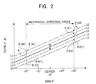
- Fig. 2 shows arithmetic processing when the detection output exceeds an upper limit value or falls below a lower limit value.
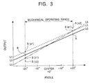
- Fig. 3 shows arithmetic processing when the detection output which has exceeded the upper limit value falls below the lower limit value.
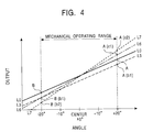
- Fig. 4 shows arithmetic processing when the detection output which has fallen below the lower limit value exceeds the upper limit value.
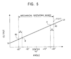
- Fig. 5 shows arithmetic processing when dead zones are provided.
- an arithmetic unit 1 for correcting a detection output contains an A/D converter 3 connected to a detector 2, a main memory 4, and a controller 5.
- the detector 2 can be of any type as long as it has a linear input/output characteristic.
- the detector 2 can be a rotating-type or sliding-type resistor, a magnetic detector such as a Hall element or a magnetoresistive sensor, or a piezoelectric element such as a PZT (Pb(Zr-Ti)O 3 ) element.
- the A/D converter 3 has a function for allocating a predetermined voltage level using a predetermined resolution, such as 256 discrete levels (2 8 discrete levels) or 1024 discrete levels (2 10 discrete levels), and, in accordance with the allocation, converting an analog output Ax of the detector 2 into a digital output Dx.
- a predetermined resolution such as 256 discrete levels (2 8 discrete levels) or 1024 discrete levels (2 10 discrete levels)
- converting an analog output Ax of the detector 2 into a digital output Dx When the output of the detector 2 ranges from 0.5 V to 4.5 V, the range of convertible voltage (operating range) of the A/D converter 3 is 0 V to 5V. In such a manner, the output range of the detector 2 is set to fit into the operating range of the A/D converter 3.
- the main memory 4 includes a ROM (Read Only Memory) or a RAM (Random Access Memory).
- the controller 5 is formed mainly by a CPU (Central Processing Unit) and contains therein a first register (memory), a second register (memory), and a third register (memory).
- the controller 5 performs processing control of the A/D converter 3 and the main memory 4 and communication control with external circuits.
- Fig. 2 shows an input/output characteristic of a rotating-type resistor as an example of the detector 2.
- the horizontal axis represents a rotation angle of the operation knob
- the vertical axis represents an output voltage of an output unit of the operation knob.
- a voltage which is output in proportion to the resistance, which varies in accordance with the rotation of the operation knob is shown.
- the center of the detector 2 is set to zero degrees, and the operation knob can be rotated within a range of -20 degrees to +20 degrees around the center.
- an output unit 2a of the detector 2 outputs a lower limit value B (such as 0.5 V).
- the output unit 2a outputs an upper limit value A (such as 4.5 V).
- the input/output characteristic of the detector 2 is linear (straight line).
- the detector 2 outputs an analog output Ax which is in proportion to the rotation angle of the operation knob.
- the ROM of the main memory 4 stores beforehand the upper limit value A of the detector 2 when the operation knob is rotated +20 degrees and the lower limit value B of the detector 2 when the operation knob is rotated -20 degrees as digital values.
- the input/output characteristic is indicated by a straight line (line L0-L0) passing through the upper limit value A and the lower limit value B.
- the upper limit value A and the lower limit value B are stored as initial values of the detector 2 in the main memory 4.
- the upper limit value A and the lower limit value B can be averages taken from values obtained by measuring detection outputs of a plurality of detectors 2 of the same type. Alternatively, the upper limit value A and the lower limit value B can be obtained for individual detectors 2 by individually measuring detection outputs of the detectors 2.
- the controller 5 When the arithmetic unit 1 with the detector 2 is turned ON, the controller 5 reads the upper limit value A and the lower limit value B from the main memory 4 and stores the upper limit value A and the lower limit value B in the first register and the second register, respectively, in the controller 5.
- the controller 5 activates the A/D converter 3 to convert an analog output Ax output from the output unit 2a of the detector 2 into an output (digital value) Dx.
- the digitally-converted output Dx is stored in the third register in the controller 5.
- the controller 5 causes the A/D converter 3 to convert an analog output Ax from the detector 2 into a digital output Dx at a predetermined sampling time and overwrites the contents of the third register by the digitally-converted output Dx. This operation is repeated.
- the contents of the first register, namely, the upper limit value A, and the contents of the second register, namely, the lower limit value B, are each compared with the contents of the third register, namely, the digital output Dx from the detector.
- n 8 that is, when the A/D converter 3 is an eight-bit A/D converter, the values between the upper limit value A and the lower limit value B are allocated using a resolution of 256 (00 to FF), and in accordance with the allocation, the output of the detector 2 is converted into one of the values from 00 to FF.
- the operation output D is output as a final output value of the detector 2 through a bus line to various external circuits.
- the arithmetic unit 1 performs processing described below.
- the controller 5 updates the contents of the first register (upper limit value A) by overwriting the contents by the value A(a1), which is the digital output Dx exceeding the upper limit value A, and the value A(a1) is regarded as a new upper limit value.
- the controller 5 assumes a straight line passing through the new upper limit value A(a1) as a virtual line L1-L1. It is assumed that the slope of the virtual line L1-L1 is the same as that of the straight line L0-L0 representing the initial input/output characteristic of the detector 2.
- the controller 5 computes a corresponding lower limit value B(a1) when the operation knob is rotated -20 degrees in accordance with the virtual line L1-L1 and overwrites the contents of the second register (lower limit value B) by the new lower limit value B(a1), thus updating the lower limit value.
- the controller 5 corrects the subsequent digital output Dx output from the detector 2.
- the controller 5 When the operation knob is further operated, and when the digital output Dx becomes a value A(a2) exceeding the new upper limit value A(a1), the controller 5 performs processing similar to the above using the new upper limit value A(a2).
- the controller 5 computes a new lower limit value B(a2) in accordance with the new upper limit value A(a2) and a virtual line L2-L2 passing through the new upper limit value A(a2).
- the controller 5 overwrites the contents of the first and second registers by the new upper limit value A(a2) and the lower limit value B(a2), thus updating the upper limit value and the lower limit value.
- the controller 5 corrects the subsequent digital output Dx from the detector 2.
- the foregoing updating processing is repeated every time the digital output Dx exceeding the upper limit value A stored in the first register is input.
- the arithmetic unit 1 can perform correction in accordance with a new virtual line which represents the actual input/output characteristic of the detector 2, and the accuracy of the operation output D can be improved.
- the controller 5 overwrites the contents of the second register by the new lower limit value B(c1), assumes a straight line passing through the upper limit value A(a1) and the new lower limit value B(c1) as a virtual line L5-L5, and performs correction in accordance with the new straight line as the input/output characteristic of the detector 2.
- the controller 5 corrects the digital output Dx of the detector 2 in accordance with the new upper limit value A(al), the new lower limit value B(c1), and equation (2).
- the operation output D is output as a final output of the detector 2 to various external circuits through a bus line.
- the controller 5 performs processing similar to the above around the lower limit value B. Specifically, the controller 5 overwrites the contents of the second register (lower limit value B) by the new lower limit value B(b1).
- the controller 5 assumes a virtual line L4-L4 passing through the new lower limit value B(b1) (see Fig. 2) and, in accordance with the virtual line L4-L4, computes an upper limit value A(b1) when the operation knob is operated +20 degrees.
- the controller 5 overwrites the contents of the first and second registers by the new upper limit value A(b1) and the new lower limit value B(b1). In accordance with the new upper limit value A(b1), the new lower limit value B(b1), and equation (2), the controller 5 corrects the subsequently-input digital output Dx.
- the above updating processing is repetitively performed every time the digital output Dx falling below the lower limit value B stored in the second register is input.
- the controller 5 overwrites the contents of the first register by the new upper limit value A(c1), assumes a straight line (virtual line L6-L6) passing through the new upper limit value A(c1) and the lower limit value B(b1), and performs correction in accordance with the new virtual line L6-L6 which is regarded as the input/output characteristic of the detector 2.
- the digital output Dx of the detector 2 is corrected in accordance with the new upper limit value A(c1), the new lower limit value B(b1), and equation (2).
- the resulting operation output D is output as a final output of the detector 2 to various external circuits through the bus line.
- the controller 5 When the digital output Dx of the detector 2 exceeds the overwritten upper limit value A(c1) and falls below the lower limit value B(b1), the controller 5 again overwrites the upper limit value A(c1) by a new upper limit value A(c2) and the lower limit value B(b1) by a new lower limit value B(b2), thus updating the upper and lower limit values. Processing similar to the above is performed in accordance with a newly assumed virtual line L7-L7 (straight line).
- the use of the arithmetic unit 1 achieves correction in accordance with the input/output characteristic approximating to the actual input/output characteristic of the detector 2.
- the accuracy of the operation output (corrected value) D obtained by correcting the digital output Dx of the detector 2 using the upper limit value A and the lower limit value B can be improved.
- the internal mechanical characteristics may vary.
- the upper limit value A and the lower limit value B after the variation greatly differ from the initial upper limit value A and the initial lower limit value B stored in the main memory 4.
- the operation output D with respect to the input operation of the detector 2 (the operation of the operation knob) can be obtained in accordance with a proportional distribution based on the new upper limit value A and the new lower limit value B.
- the digital output Dx of the detector 2 more frequently exceeds the upper limit value A and/or falls below the lower limit value B. Accordingly, the accuracy of the operation output D can be improved.
- the correction operation is performed without being noticed by a user, that is, the correction operation is automatically performed by internal processing of the arithmetic unit 1 while the user is operating the operation knob. Thus, no burden in put on the user.
- the initial upper limit value A and the initial lower limit value B stored in the main memory 4 tend to be an upper limit value of the operating range of the detector 2 (for example, digital output Dx when +20 degrees is detected) and a lower limit value of the operating range (digital output Dx when -20 degrees is detected).
- the digital output Dx rarely exceeds/falls below the limit values of the operating range particularly when the detector 2 is new.
- the arithmetic unit 1 cannot sufficiently perform the updating, and it becomes difficult to improve the correction accuracy of the operation output D.
- A0 represents an actual upper limit value obtained from the A/D converter 3 when the operating range of the detector 2 is at the upper limit
- B0 represents an actual lower limit value obtained from the A/D converter 3 when the operating range of the detector 2 is at the lower limit.
- a dead zone ⁇ of a predetermined constant is provided at a lower side of the upper limit value A
- a dead zone ⁇ of a predetermined constant is provided at an upper side of the lower limit value B.
- the dead zone ⁇ is provided at each of the lower side of the upper limit value A and at the upper side of the lower limit value B.
- the upper limit value A is A0 - ⁇
- the lower limit value B is B0 + ⁇ .
- the upper limit value A can be set to a value less than the actual upper limit value A0 of the detector 2
- the lower limit value B can be set to a value greater than the actual lower limit value B0 of the detector 2.
- the digital output Dx more frequently updates the upper limit value A and the lower limit value B.
- an updated value can be obtained by subtracting the dead zone ⁇ from the detected value, for the upper limit value, or adding the dead zone ⁇ to the detected value, for the lower limit value.
Landscapes
- Engineering & Computer Science (AREA)
- Human Computer Interaction (AREA)
- Manufacturing & Machinery (AREA)
- Physics & Mathematics (AREA)
- General Physics & Mathematics (AREA)
- Automation & Control Theory (AREA)
- Indication And Recording Devices For Special Purposes And Tariff Metering Devices (AREA)
- Analogue/Digital Conversion (AREA)
- Transmission And Conversion Of Sensor Element Output (AREA)
- Measurement Of Current Or Voltage (AREA)
Abstract
Description
Claims (8)
- An arithmetic unit for allocating a linear analog output obtained from detection means using a predetermined number of discrete levels (2n), comprising:A/D conversion means for converting the analog output from the detection means into a digital value (Dx); memory means for storing an upper limit value A and a lower limit value B of the digital value (Dx) as predetermined values; anda controller for performing the following processing steps:(1) when the digital value (Dx) is A(a1), which exceeds the upper limit value A, updating the upper limit value stored in the memory means to A(a1);(2) computing a virtual lower limit value B(a1) from the upper limit value A(a1) in accordance with the slope of a linear function determined by the preset upper limit value A and the preset lower limit value B and updating the lower limit value stored in the memory means to the lower limit value B(a1); and(3) computing an operation output D by calculating the following equation with respect to a subsequently-obtained digital value (Dx):
- The arithmetic unit for correcting the detection output according to Claim 1, wherein, every time the digital value (Dx) exceeds the upper limit value A(a1), the processing steps (1), (2), and (3) are performed in accordance with a new upper limit value.
- The arithmetic unit for correcting the detection output according to Claim 1, wherein, when the digital value (Dx) is B(c1), which falls below the lower limit value B, the following processing steps are performed:(4) updating the lower limit value stored in the memory means to B(c1); and(5) calculating the following equation using the updated upper limit value and the updated lower limit value:
- An arithmetic unit for allocating a linear analog output obtained from detection means using a predetermined number of discrete levels (2n), comprising:A/D conversion means for converting the analog output from the detection means into a digital value (Dx);memory means for storing an upper limit value A and a lower limit value B of the digital value (Dx) as predetermined values; anda controller for performing the following processing steps:(1) when the digital value (Dx) is B(b1), which falls below the lower limit value B, updating the lower limit value stored in the memory means to B(b1);(2) computing a virtual upper limit value A(b1) from the lower limit value B(b1) in accordance with the slope of a linear function determined by the preset upper limit value A and the preset lower limit value B and updating the upper limit value stored in the memory means to A(b1); and(3) computing an operation output D by calculating the following equation with respect to a subsequently-obtained digital value (Dx):
- The arithmetic unit for correcting the detection output according to Claim 4, wherein, every time the digital value (Dx) falls below the lower limit value B(b1), the processing steps (1), (2), and (3) are performed in accordance with a new lower limit value.
- The arithmetic unit for correcting the detection output according to Claim 4, wherein, when the digital value (Dx) is A(c1), which exceeds the upper limit value A, the following processing steps are performed:(4) updating the upper limit value stored in the memory means to A(c1); and(5) calculating the following equation using the updated upper limit value and the updated lower limit value:
- The arithmetic unit for correcting the detection output according to Claim 1, wherein, in a case when A0 represents an actual upper limit value obtained from the A/D conversion means when an operating range of the detection means is at an upper limit and when B0 represents an actual lower limit value obtained from the A/D conversion means when the operating range of the detection means is at a lower limit, the upper limit value A and the lower limit value B stored in the memory means are values taking into consideration a predetermined dead zone α, whereby A = A0 - α and B = B0 + α, and
when updating the upper limit value or the lower limit value, an updated value is obtained by subtracting the dead zone α from the detected value, for the upper limit value, or adding the dead zone α to the detected value, for the lower limit value. - The arithmetic unit for correcting the detection output according to Claim 4, wherein, in a case when A0 represents an actual upper limit value obtained from the A/D conversion means when an operating range of the detection means is at an upper limit and when B0 represents an actual lower limit value obtained from the A/D conversion means when the operating range of the detection means is at a lower limit, the upper limit value A and the lower limit value B stored in the memory means are values taking into consideration a predetermined dead zone α, whereby A = A0 - α and B = B0 + α, and
when updating the upper limit value or the lower limit value, an updated value is obtained by subtracting the dead zone α from the detected value, for the upper limit value, or adding the dead zone α to the detected value, for the lower limit value.
Applications Claiming Priority (2)
| Application Number | Priority Date | Filing Date | Title |
|---|---|---|---|
| JP2001097877 | 2001-03-30 | ||
| JP2001097877A JP3866526B2 (en) | 2001-03-30 | 2001-03-30 | Detection output arithmetic unit |
Publications (3)
| Publication Number | Publication Date |
|---|---|
| EP1260888A2 true EP1260888A2 (en) | 2002-11-27 |
| EP1260888A3 EP1260888A3 (en) | 2004-03-31 |
| EP1260888B1 EP1260888B1 (en) | 2007-06-20 |
Family
ID=18951594
Family Applications (1)
| Application Number | Title | Priority Date | Filing Date |
|---|---|---|---|
| EP02251955A Expired - Lifetime EP1260888B1 (en) | 2001-03-30 | 2002-03-19 | Arithmetic unit for correcting detection output in which corrected operation output is sensitive to mechanical factors |
Country Status (4)
| Country | Link |
|---|---|
| US (1) | US6868430B2 (en) |
| EP (1) | EP1260888B1 (en) |
| JP (1) | JP3866526B2 (en) |
| DE (1) | DE60220742T2 (en) |
Families Citing this family (2)
| Publication number | Priority date | Publication date | Assignee | Title |
|---|---|---|---|---|
| US7310470B2 (en) * | 2005-04-14 | 2007-12-18 | Tyco Electronics Corporation | Optical fiber repair apparatus with adjustable guide member and methods for using the same |
| JP6557086B2 (en) * | 2015-07-31 | 2019-08-07 | ファナック株式会社 | Control device with rotary switch |
Family Cites Families (9)
| Publication number | Priority date | Publication date | Assignee | Title |
|---|---|---|---|---|
| US4841209A (en) * | 1987-11-25 | 1989-06-20 | United Technologies Corporation | Actuator control system with displacement sensor fault detection |
| US5245695A (en) * | 1991-06-12 | 1993-09-14 | American Neuralogix Inc. | Fuzzy microcontroller |
| US5278558A (en) * | 1992-07-21 | 1994-01-11 | Rockwell International Corporation | High accuracy digital to analog converter adjustment method and apparatus |
| US5345235A (en) * | 1993-04-12 | 1994-09-06 | Motorola, Inc. | Scaled reference analog-to-digital conversion circuitry and method of operation |
| JP3231182B2 (en) | 1994-05-25 | 2001-11-19 | アルプス電気株式会社 | Operation input device |
| US5748672A (en) * | 1995-08-11 | 1998-05-05 | Cenrad, Inc. | System for measuring jitter in a non-binary digital signal |
| US6240381B1 (en) * | 1998-02-17 | 2001-05-29 | Fonix Corporation | Apparatus and methods for detecting onset of a signal |
| EP0942271A1 (en) | 1998-03-10 | 1999-09-15 | Oxford Instruments (Uk) Limited | Improvements in resistance thermometry |
| US20040136379A1 (en) * | 2001-03-13 | 2004-07-15 | Liao Raymond R | Method and apparatus for allocation of resources |
-
2001
- 2001-03-30 JP JP2001097877A patent/JP3866526B2/en not_active Expired - Fee Related
-
2002
- 2002-03-19 EP EP02251955A patent/EP1260888B1/en not_active Expired - Lifetime
- 2002-03-19 DE DE60220742T patent/DE60220742T2/en not_active Expired - Lifetime
- 2002-03-27 US US10/108,525 patent/US6868430B2/en not_active Expired - Lifetime
Also Published As
| Publication number | Publication date |
|---|---|
| EP1260888B1 (en) | 2007-06-20 |
| DE60220742D1 (en) | 2007-08-02 |
| JP3866526B2 (en) | 2007-01-10 |
| DE60220742T2 (en) | 2008-03-06 |
| US6868430B2 (en) | 2005-03-15 |
| US20020169807A1 (en) | 2002-11-14 |
| EP1260888A3 (en) | 2004-03-31 |
| JP2002300033A (en) | 2002-10-11 |
Similar Documents
| Publication | Publication Date | Title |
|---|---|---|
| US6188340B1 (en) | Sensor adjusting circuit | |
| US6466889B1 (en) | Method and apparatus for determining absolute position of displacement and angle sensors | |
| US7671777B2 (en) | AD converter | |
| US7787033B2 (en) | Apparatus and method for determining temperature of an active pixel imager and correcting temperature induced variations in an imager | |
| US5764542A (en) | Noise filtering utilizing running average | |
| US7319418B2 (en) | Sensor with multiplex data output | |
| US4463272A (en) | Automatic drift correction | |
| US20090281760A1 (en) | Apparatus and method for determining a temperature of a temperature sensing element | |
| WO1998002721A2 (en) | Calibration of a sensor with temperature variations | |
| US6260054B1 (en) | Reciprocal generator using piece-wise-linear segments of varying width with floating-point format | |
| EP1260888B1 (en) | Arithmetic unit for correcting detection output in which corrected operation output is sensitive to mechanical factors | |
| US6744389B2 (en) | A/D-converter with lookup table | |
| US6861967B2 (en) | Non-linearity correcting method and device for A/D conversion output data | |
| JPS62261070A (en) | measuring device | |
| US9127966B2 (en) | Physical quantity detection apparatus and inspection method of physical quantity detection apparatus | |
| KR100951545B1 (en) | Digital temperature and humidity sensor | |
| WO2002001850A1 (en) | Gamma correction device | |
| JP3427535B2 (en) | Characteristic variation correction method | |
| US20220318010A1 (en) | Physical Quantity Detection Device | |
| CN120448674B (en) | Scanning valve pressure compensation model correction method, device, equipment and medium | |
| JPS61138133A (en) | Load cell unit | |
| US6570380B2 (en) | Non-linear hall IC | |
| JPH0550838U (en) | Analog voltage digital converter | |
| JPH0585842B2 (en) | ||
| JP4340863B2 (en) | Conversion circuit calibration method and signal input circuit |
Legal Events
| Date | Code | Title | Description |
|---|---|---|---|
| PUAI | Public reference made under article 153(3) epc to a published international application that has entered the european phase |
Free format text: ORIGINAL CODE: 0009012 |
|
| AK | Designated contracting states |
Kind code of ref document: A2 Designated state(s): AT BE CH CY DE DK ES FI FR GB GR IE IT LI LU MC NL PT SE TR |
|
| AX | Request for extension of the european patent |
Free format text: AL;LT;LV;MK;RO;SI |
|
| PUAL | Search report despatched |
Free format text: ORIGINAL CODE: 0009013 |
|
| AK | Designated contracting states |
Kind code of ref document: A3 Designated state(s): AT BE CH CY DE DK ES FI FR GB GR IE IT LI LU MC NL PT SE TR |
|
| AX | Request for extension of the european patent |
Extension state: AL LT LV MK RO SI |
|
| RIC1 | Information provided on ipc code assigned before grant |
Ipc: 7H 03M 1/18 B Ipc: 7G 05B 19/35 A Ipc: 7G 05B 9/02 B |
|
| 17P | Request for examination filed |
Effective date: 20040503 |
|
| AKX | Designation fees paid |
Designated state(s): DE GB |
|
| GRAP | Despatch of communication of intention to grant a patent |
Free format text: ORIGINAL CODE: EPIDOSNIGR1 |
|
| GRAS | Grant fee paid |
Free format text: ORIGINAL CODE: EPIDOSNIGR3 |
|
| GRAA | (expected) grant |
Free format text: ORIGINAL CODE: 0009210 |
|
| AK | Designated contracting states |
Kind code of ref document: B1 Designated state(s): DE GB |
|
| REG | Reference to a national code |
Ref country code: GB Ref legal event code: FG4D |
|
| REF | Corresponds to: |
Ref document number: 60220742 Country of ref document: DE Date of ref document: 20070802 Kind code of ref document: P |
|
| PLBE | No opposition filed within time limit |
Free format text: ORIGINAL CODE: 0009261 |
|
| STAA | Information on the status of an ep patent application or granted ep patent |
Free format text: STATUS: NO OPPOSITION FILED WITHIN TIME LIMIT |
|
| 26N | No opposition filed |
Effective date: 20080325 |
|
| REG | Reference to a national code |
Ref country code: DE Ref legal event code: R082 Ref document number: 60220742 Country of ref document: DE Representative=s name: SCHMITT-NILSON SCHRAUD WAIBEL WOHLFROM PATENTA, DE |
|
| REG | Reference to a national code |
Ref country code: DE Ref legal event code: R082 Ref document number: 60220742 Country of ref document: DE Representative=s name: SCHMITT-NILSON SCHRAUD WAIBEL WOHLFROM PATENTA, DE Ref country code: DE Ref legal event code: R081 Ref document number: 60220742 Country of ref document: DE Owner name: ALPS ALPINE CO., LTD., JP Free format text: FORMER OWNER: ALPS ELECTRIC CO., LTD., TOKIO/TOKYO, JP |
|
| PGFP | Annual fee paid to national office [announced via postgrant information from national office to epo] |
Ref country code: DE Payment date: 20200320 Year of fee payment: 19 Ref country code: GB Payment date: 20200323 Year of fee payment: 19 |
|
| REG | Reference to a national code |
Ref country code: DE Ref legal event code: R119 Ref document number: 60220742 Country of ref document: DE |
|
| GBPC | Gb: european patent ceased through non-payment of renewal fee |
Effective date: 20210319 |
|
| PG25 | Lapsed in a contracting state [announced via postgrant information from national office to epo] |
Ref country code: GB Free format text: LAPSE BECAUSE OF NON-PAYMENT OF DUE FEES Effective date: 20210319 Ref country code: DE Free format text: LAPSE BECAUSE OF NON-PAYMENT OF DUE FEES Effective date: 20211001 |