EP1260616A1 - Polycrystalline diamond thin film, photocathode and electron tube using it - Google Patents
Polycrystalline diamond thin film, photocathode and electron tube using it Download PDFInfo
- Publication number
- EP1260616A1 EP1260616A1 EP01906198A EP01906198A EP1260616A1 EP 1260616 A1 EP1260616 A1 EP 1260616A1 EP 01906198 A EP01906198 A EP 01906198A EP 01906198 A EP01906198 A EP 01906198A EP 1260616 A1 EP1260616 A1 EP 1260616A1
- Authority
- EP
- European Patent Office
- Prior art keywords
- light
- photocathode
- diamond
- absorbing layer
- polycrystal diamond
- Prior art date
- Legal status (The legal status is an assumption and is not a legal conclusion. Google has not performed a legal analysis and makes no representation as to the accuracy of the status listed.)
- Ceased
Links
- 229910003460 diamond Inorganic materials 0.000 title claims abstract description 93
- 239000010432 diamond Substances 0.000 title claims abstract description 93
- 239000010409 thin film Substances 0.000 title claims abstract description 20
- 239000002245 particle Substances 0.000 claims abstract description 30
- 238000001237 Raman spectrum Methods 0.000 claims abstract description 11
- 238000001069 Raman spectroscopy Methods 0.000 claims abstract description 7
- 239000000758 substrate Substances 0.000 claims description 15
- 230000004913 activation Effects 0.000 claims description 13
- 239000000463 material Substances 0.000 claims description 12
- UFHFLCQGNIYNRP-UHFFFAOYSA-N Hydrogen Chemical compound [H][H] UFHFLCQGNIYNRP-UHFFFAOYSA-N 0.000 claims description 5
- 229910052739 hydrogen Inorganic materials 0.000 claims description 5
- 239000001257 hydrogen Substances 0.000 claims description 5
- KRHYYFGTRYWZRS-UHFFFAOYSA-M Fluoride anion Chemical compound [F-] KRHYYFGTRYWZRS-UHFFFAOYSA-M 0.000 claims description 3
- 229910052783 alkali metal Inorganic materials 0.000 claims description 3
- 150000001340 alkali metals Chemical class 0.000 claims description 3
- 238000006243 chemical reaction Methods 0.000 description 25
- 239000012808 vapor phase Substances 0.000 description 8
- 239000010408 film Substances 0.000 description 6
- 238000005268 plasma chemical vapour deposition Methods 0.000 description 6
- 230000035945 sensitivity Effects 0.000 description 5
- 230000002349 favourable effect Effects 0.000 description 4
- 239000007789 gas Substances 0.000 description 4
- 239000000376 reactant Substances 0.000 description 4
- 239000004065 semiconductor Substances 0.000 description 4
- VYPSYNLAJGMNEJ-UHFFFAOYSA-N Silicium dioxide Chemical compound O=[Si]=O VYPSYNLAJGMNEJ-UHFFFAOYSA-N 0.000 description 2
- 239000013078 crystal Substances 0.000 description 2
- 238000004519 manufacturing process Methods 0.000 description 2
- 238000000034 method Methods 0.000 description 2
- 238000012544 monitoring process Methods 0.000 description 2
- 239000000126 substance Substances 0.000 description 2
- OKTJSMMVPCPJKN-UHFFFAOYSA-N Carbon Chemical compound [C] OKTJSMMVPCPJKN-UHFFFAOYSA-N 0.000 description 1
- 230000005540 biological transmission Effects 0.000 description 1
- 229910052792 caesium Inorganic materials 0.000 description 1
- WUKWITHWXAAZEY-UHFFFAOYSA-L calcium difluoride Chemical compound [F-].[F-].[Ca+2] WUKWITHWXAAZEY-UHFFFAOYSA-L 0.000 description 1
- 229910001634 calcium fluoride Inorganic materials 0.000 description 1
- 229910052799 carbon Inorganic materials 0.000 description 1
- 239000000470 constituent Substances 0.000 description 1
- 230000007423 decrease Effects 0.000 description 1
- 238000005516 engineering process Methods 0.000 description 1
- 238000004050 hot filament vapor deposition Methods 0.000 description 1
- 238000003384 imaging method Methods 0.000 description 1
- 239000012535 impurity Substances 0.000 description 1
- 230000010354 integration Effects 0.000 description 1
- 229910001635 magnesium fluoride Inorganic materials 0.000 description 1
- 230000003287 optical effect Effects 0.000 description 1
- 238000000206 photolithography Methods 0.000 description 1
- 229910052700 potassium Inorganic materials 0.000 description 1
- 229910052701 rubidium Inorganic materials 0.000 description 1
- 229910052594 sapphire Inorganic materials 0.000 description 1
- 239000010980 sapphire Substances 0.000 description 1
- 239000000377 silicon dioxide Substances 0.000 description 1
- 229910052708 sodium Inorganic materials 0.000 description 1
- 238000010183 spectrum analysis Methods 0.000 description 1
Images



Classifications
-
- H—ELECTRICITY
- H01—ELECTRIC ELEMENTS
- H01J—ELECTRIC DISCHARGE TUBES OR DISCHARGE LAMPS
- H01J43/00—Secondary-emission tubes; Electron-multiplier tubes
- H01J43/04—Electron multipliers
- H01J43/06—Electrode arrangements
- H01J43/08—Cathode arrangements
-
- H—ELECTRICITY
- H01—ELECTRIC ELEMENTS
- H01J—ELECTRIC DISCHARGE TUBES OR DISCHARGE LAMPS
- H01J1/00—Details of electrodes, of magnetic control means, of screens, or of the mounting or spacing thereof, common to two or more basic types of discharge tubes or lamps
- H01J1/02—Main electrodes
- H01J1/34—Photo-emissive cathodes
-
- H—ELECTRICITY
- H01—ELECTRIC ELEMENTS
- H01J—ELECTRIC DISCHARGE TUBES OR DISCHARGE LAMPS
- H01J40/00—Photoelectric discharge tubes not involving the ionisation of a gas
- H01J40/02—Details
- H01J40/04—Electrodes
- H01J40/06—Photo-emissive cathodes
-
- H—ELECTRICITY
- H01—ELECTRIC ELEMENTS
- H01J—ELECTRIC DISCHARGE TUBES OR DISCHARGE LAMPS
- H01J2201/00—Electrodes common to discharge tubes
- H01J2201/34—Photoemissive electrodes
- H01J2201/342—Cathodes
- H01J2201/3421—Composition of the emitting surface
-
- H—ELECTRICITY
- H01—ELECTRIC ELEMENTS
- H01J—ELECTRIC DISCHARGE TUBES OR DISCHARGE LAMPS
- H01J2231/00—Cathode ray tubes or electron beam tubes
- H01J2231/50—Imaging and conversion tubes
- H01J2231/50005—Imaging and conversion tubes characterised by form of illumination
- H01J2231/5001—Photons
- H01J2231/50015—Light
- H01J2231/50021—Ultraviolet
-
- Y—GENERAL TAGGING OF NEW TECHNOLOGICAL DEVELOPMENTS; GENERAL TAGGING OF CROSS-SECTIONAL TECHNOLOGIES SPANNING OVER SEVERAL SECTIONS OF THE IPC; TECHNICAL SUBJECTS COVERED BY FORMER USPC CROSS-REFERENCE ART COLLECTIONS [XRACs] AND DIGESTS
- Y10—TECHNICAL SUBJECTS COVERED BY FORMER USPC
- Y10T—TECHNICAL SUBJECTS COVERED BY FORMER US CLASSIFICATION
- Y10T428/00—Stock material or miscellaneous articles
- Y10T428/30—Self-sustaining carbon mass or layer with impregnant or other layer
Definitions
- the present invention relates to a polycrystal diamond thin film which can absorb a predetermined wavelength of light and emit a photoelectron, and a photocathode and electron tube using the same.
- Photocathodes used for detecting a predetermined wavelength of light to be detected, and electron tubes equipped therewith have conventionally been known.
- a photocathode has a light-absorbing layer for absorbing a predetermined wavelength of light and emitting a photoelectron. The light to be detected is made incident on the light-absorbing layer and then is converted into a photoelectron, whereby it can be detected. While various semiconductor materials are used for the light-absorbing layer, Japanese Patent Application Laid-Open No. HEI 10-149761 discloses polycrystal diamond as a material having a high photoelectric conversion quantum efficiency with respect to ultraviolet light.
- the inventors carried out diligent studies in order to improve the photoelectric conversion quantum efficiency of polycrystal diamond thin films and, as a result, have found that the photoelectric conversion quantum efficiency of a polycrystal diamond thin film is greatly influenced by its film quality.
- a Raman spectrum obtained by Raman spectroscopy is used in general.
- Fig. 7 is a graph showing an example of Raman spectrum.
- a peak indicative of a diamond component occurs near a wave number of 1335 cm -1
- a peak indicative of a non-diamond component occurs near a wave number of 1580 cm -1 .
- P1 be the peak intensity near a wave number of 1335 cm -1
- P2 be the peak intensity near a wave number of 1580 cm -1 in the Raman spectrum
- P2/P1 is defined as "non-diamond ratio" indicative of the crystallinity in this specification.
- the polycrystal diamond thin film in accordance with the present invention is characterized in that it has an average particle size of at least 1.5 ⁇ m; and that, in a Raman spectrum obtained by Raman spectroscopy, a peak intensity near a wave number of 1580 cm -1 has a ratio of 0.2 or less with respect to a peak intensity near a wave number of 1335 cm -1 .
- polycrystal diamond has a particle size of at least 1.5 ⁇ m, while the non-diamond ratio is set to 0.2 or less, whereby a polycrystal diamond thin film having a high photoelectric conversion quantum efficiency is realized.
- the photocathode in accordance with the present invention is a photocathode comprising a light-absorbing layer for emitting an electron in response to the quantity of light incident thereon, the light-absorbing layer being made of polycrystal diamond or a material mainly composed of polycrystal diamond; wherein the polycrystal diamond has an average particle size of at least 1.5 ⁇ m; and wherein, in a Raman spectrum of the polycrystal diamond obtained by Raman spectroscopy, a peak intensity near a wave number of 1580 cm -1 has a ratio of 0.2 or less with respect to a peak intensity near a wave number of 1335 cm -1 .
- the photocathode may be characterized in that the surface of the light-absorbing layer is terminated with hydrogen.
- the surface of the light-absorbing layer is terminated with hydrogen as such, the light-absorbing layer surface can lower its work function, so as to emit photoelectrons more easily.
- the photocathode may further comprise an activation layer, disposed on the surface of the light-absorbing layer, for lowering electron affinity.
- an activation layer disposed on the surface of the light-absorbing layer as such, the light-absorbing layer surface can lower its electron affinity, so as to emit photoelectrons more easily.
- the activation layer may comprise an alkali metal or an oxide or fluoride thereof.
- the activation layer can be formed easily.
- the polycrystal diamond may have a conductivity of p-type.
- the polycrystal diamond can lower its resistance, so as to emit photoelectrons more easily.
- the photocathode may further comprise a substrate for supporting the light-absorbing layer.
- the photocathode comprises a substrate as such, the light-absorbing layer, which is a thin film likely to be damaged, can enhance its strength.
- the substrate may be transparent to light having a wavelength of 200 nm or less.
- the substrate is transparent to light having a wavelength of 200 nm or less, the light entering from the substrate side can be detected.
- the electron tube in accordance with the present invention comprises an entrance window transparent to a predetermined wavelength of incident light; the above-mentioned photocathode; an envelope accommodating the photocathode and supporting the entrance window; and an anode, accommodated in the envelope, for collecting a photoelectron emitted from the photocathode. Since the above-mentioned photocathode is used as a photoelectric converter, an electron tube having a favorable sensitivity can be realized.
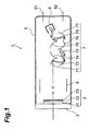
- Fig. 1 is a view showing an electron tube 1 in accordance with an embodiment.
- the electron tube 1 comprises a photocathode 2 for absorbing a predetermined wavelength of light and emitting photoelectrons, an electron multiplier 7 for multiplying the emitted photoelectrons, an anode 4 for collecting the multiplied photoelectron, and an envelope 5 for accommodating these parts.
- the entrance window 3 is constituted by a material, such as MF 2 , which is transparent to ultraviolet light which is light to be detected.
- the photocathode 2 is disposed near the entrance window 3; whereas the photocathode 2, the electron multiplier 7 constituted by a plurality of dynodes 71 to 78, and the anode 4 are disposed substantially parallel to the entrance optical axis of the light to be detected.
- the end part of container 5 on the side having the anode 4 is provided with stem pins 81, 82 for taking out the electrons collected by the anode 4 from within the envelope 5.
- a focusing electrode 6 for efficiently converging the photoelectrons emitted by the photocathode 2 onto the electron multiplier 7.
- the envelope 5 is evacuated so as to attain an ultrahigh vacuum of about 1 x 10 -10 Torr therein.
- the photocathode 2 comprises a substrate 21 transparent to ultraviolet light which is light to be detected, a light-absorbing layer 22 made of polycrystal diamond disposed on the substrate 21, and an activation layer 23 disposed on the surface of the light-absorbing layer 22.
- the photocathode 2 is disposed within the envelope 5 such that the substrate 21 and the entrance window 3 oppose each other.
- the substrate 21 and the entrance window 3 can be constructed as a single member from the same material.
- the material for the substrate 21 is CaF 2 , MgF 2 , silica, sapphire, or the like which is transparent to ultraviolet light; whereas an alkali metal such as Cs, Rb, K, Na, or Li, or an oxide or fluoride thereof is used as the material for the activation layer 23.
- the polycrystal diamond constituting the light-absorbing layer 22, which is a characteristic feature of this embodiment, will now be explained in detail.
- the polycrystal diamond has a conductivity of p-type, and is terminated with hydrogen in the vicinity of its boundary with respect to the activation layer.
- crystals constituting the polycrystal diamond have an average particle size of at least 1.5 ⁇ m although their respective particle sizes are not constant, and a non-diamond ratio of 0.2 or less.
- the Raman spectrum employed as a basis for calculating this non-diamond ratio is one obtained by Raman spectral analysis using a laser light source having a spot diameter of 1 ⁇ m at a wavelength of 514.5 nm.
- Fig. 2 is a graph showing the relationship between the non-diamond ratio and photoelectric conversion quantum efficiency of the polycrystal diamond
- Fig. 3 is a graph showing the relationship between the particle size and photoelectric conversion quantum efficiency of the polycrystal diamond.
- the photoelectric conversion quantum efficiency increases as the non-diamond ratio decreases. However, the photoelectric conversion quantum efficiency does not exceed 40% even when the non-diamond ratio is lowered to 0.2 or less.
- the photoelectric conversion quantum efficiency increases as the particle size of crystals becomes greater. However, the photoelectric conversion quantum efficiency also levels off at 40% in the range where the particle size is 1.5 ⁇ m or greater.
- the photoelectric conversion quantum efficiency shown in Fig. 2 cannot be obtained in the polycrystal diamond whose particle size is smaller than 1.5 ⁇ m, even when its value of non-diamond ratio is lowered.
- the photoelectric conversion quantum efficiency shown in Fig. 3 cannot be obtained in the polycrystal diamond whose value of non-diamond ratio is greater than 0.2, even when its particle size is made greater than 1.5 ⁇ m.
- a high photoelectric conversion quantum efficiency of 40% can be obtained only in the polycrystal diamond in which both of parameters of crystallinity and particle size fall within the above-mentioned ranges.
- the light-absorbing layer 22 of the polycrystal diamond having the above-mentioned crystallinity and particle size is manufactured as follows.
- the light-absorbing layer 22 is formed on the substrate 21 by a vapor growth method (CVD) using a microwave plasma while employing CH 4 and H 2 as reactant gases.
- CVD vapor growth method
- the crystallinity of polycrystal diamond can be controlled by the carbon component ratio in the vapor-phase component when carrying out the microwave plasma CVD, whereas its particle size can be controlled by the film thickness of polycrystal diamond formed thereby.
- Fig. 4 is a graph showing the relationship between the ratio of CH 4 and H 2 contained in the vapor-phase component and the non-diamond ratio of polycrystal diamond
- Fig. 5 is a graph showing the relationship between the thickness of the polycrystal diamond thin film and its particle size.
- the non-diamond ratio is minimized when the value of CH 4 /H 2 is near 1%, and becomes greater as the value of CH 4 /H 2 increases.
- the film thickness of polycrystal diamond and its particle size are proportional to each other.
- the polycrystal diamond can be controlled so as to have a particle size of at least 1.5 ⁇ m and a non-diamond ratio of 0.2 or less.
- the method of making the electron tube 1 in accordance with this embodiment and its action will now be explained briefly.
- the substrate 21 formed with the light-absorbing layer 22 made of polycrystal diamond is accommodated in the envelope 5 together with the electron multiplier 7, anode 4, and focusing electrode 6.
- the envelope 5 is connected to an exhaust system, by which a high vacuum of 1 x 10 -10 Torr is attained, and baking is carried out, so as to evacuate the impurities from within the envelope 5.
- test light is made incident on the photocathode 2, and the activation layer 23 is formed into a favorable thickness while monitoring the photoelectron emission current.
- This electron tube 1 acts as follows.
- the light to be detected is transmitted through the entrance window 3 and enters the envelope 5.
- Thus entered light to be detected is fed into the photocathode 2, and the latter emits photoelectrons by an amount corresponding to the quantity of the light to be detected.
- emitted photoelectrons are converged by the focusing electrode 6, so as to be fed into the electron multiplier 7.
- electrons multiplied by the electron multiplier 7 are collected by the anode 4.
- the electrons collected by the anode 4 are taken out as a signal current from the envelope 5 by way of the stem pins 81, 82, which becomes a signal indicative of the light to be detected fed into the electron tube 1.
- the photocathode 2 used in the electron tube 1 of this embodiment employs polycrystal diamond having a particle size of at least 1.5 ⁇ m and a non-diamond ratio of 0.2 or less as a material for the light-absorbing layer 22. This can realize the photocathode 2 in which the photoelectric conversion quantum efficiency is high, and can enhance the sensitivity of the electron tube 1.
- the polycrystal diamond thin film acting as the light-absorbing layer 22 is formed by microwave plasma CVD using CH 4 and H 2 as reactant gases, and its surface is terminated with hydrogen. This can lower the work function of the surface of the light-absorbing layer 22, so that photoelectrons are emitted more easily, whereby the photoelectric conversion quantum efficiency can be improved.
- the photocathode 2 comprises the activation layer 23 on the surface of the light-absorbing layer 22. This can lower the electron affinity of the surface of the light-absorbing layer 22, thus making it easier to emit photoelectrons, thereby improving the photoelectric conversion quantum efficiency.
- the polycrystal diamond constituting the light-absorbing layer 22 has a conductivity of p-type. This can lower the resistance of the light-absorbing layer 22, so that the energy band in the vicinity of the surface is bent downward, by which photoelectrons can be emitted more easily, whereby the photoelectric conversion quantum efficiency can be improved.
- This embodiment is also effective in that the light-absorbing layer 22 of the photocathode 2 having a high photoelectric conversion quantum efficiency can be formed efficiently.
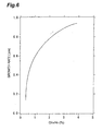
- polycrystal diamond yields a high photoelectric conversion quantum efficiency. Therefore, even when it is empirically known that polycrystal diamond having a large particle size and a low non-diamond ratio is favorable, making such a polycrystal diamond thin film has been considered unfavorable in that it involves a high cost. Namely, as the ratio of CH 4 is raised in the case where polycrystal diamond is grown by microwave plasma CVD using CH 4 and H 2 as reactant gases, the polycrystal diamond deposits faster as shown in Fig. 6, but the non-diamond ratio becomes higher as shown in Fig. 4.
- polycrystal diamond when simply based on the findings that the photoelectric conversion quantum efficiency increases if the non-diamond ratio is lowered while the particle size is made greater, polycrystal diamond must be grown for a long period of time by microwave plasma CVD in a vapor phase in which the ratio of CH 4 is low, which yields a low efficiency.
- the polycrystal diamond employed as the material for the light-absorbing layer 22 in this embodiment is defined in terms of particle size and crystallinity. Therefore, a vapor-phase component ratio at which the polycrystal diamond can be grown at the highest rate can be selected from vapor-phase component ratios (see Fig. 4) by which polycrystal diamond having a required non-diamond ratio (0.2 or less) can be formed. Also, the light-absorbing layer 22 thicker than the required film thickness (the thickness at which the particle size becomes 1.5 ⁇ m (see Fig. 5)) is kept from being formed, whereby the efficiency improves.
- the light-absorbing layer 22 is formed by use of a vapor growth method based on microwave plasma CVD in this embodiment, it may also be formed by hot filament CVD or the like. Combinations of CO and H 2 , CH 4 and CO 2 , and the like may also be used as the reactant gases without being limited to the combination of CH 4 and H 2 .
- this embodiment explains a transmission type electron tube 1 in which the light to be detected is made incident on the light-absorbing layer 22 by way of the substrate 21 whereas photoelectrons are emitted in the direction along which the light to be detected advances, it may be a reflection type electron tube in which the light to be detected enters from the activation layer side whereas photoelectrons are emitted in the direction opposite to the advancing direction of the light to be detected.
- the photocathode 2 of this embodiment is applicable not only to the electron tube 1, but also to various devices such as imaging tubes or display tubes equipped with a fluorescent substance, image intensifiers equipped with a microchannel plate and a fluorescent substance, electron bombardment tubes for accelerating electrons emitted from a photocathode and bombarding a solid-state device with thus accelerated electrons, and electron bombardment tubes for accelerating electrons emitted from a photocathode and bombarding a one- or two-dimensional position sensor device such as charge-coupled device.
- imaging tubes or display tubes equipped with a fluorescent substance image intensifiers equipped with a microchannel plate and a fluorescent substance
- electron bombardment tubes for accelerating electrons emitted from a photocathode and bombarding a solid-state device with thus accelerated electrons
- electron bombardment tubes for accelerating electrons emitted from a photocathode and bombarding a one- or two-dimensional position sensor device such as charge-coupled device.
- the present invention can realize apolycrystal diamond thin film having a high photoelectric conversion quantum efficiency. Also, a photocathode and electron tube equipped therewith can realize a photocathode and electron tube having a high sensitivity.
- the present invention can be utilized in a polycrystal diamond thin film which can absorb a predetermined wavelength of light and emit a photoelectron, and a photocathode and electron tube using the same.
Landscapes
- Common Detailed Techniques For Electron Tubes Or Discharge Tubes (AREA)
- Crystals, And After-Treatments Of Crystals (AREA)
- Chemical Vapour Deposition (AREA)
Abstract
Description
Claims (9)
- Apolycrystal diamond thin film having an average particle size of at least 1.5 µm; wherein, in a Raman spectrum obtained by Raman spectroscopy, a peak intensity near a wave number of 1580 cm-1 has a ratio of 0.2 or less with respect to a peak intensity near a wave number of 1335 cm-1.
- A photocathode comprising a light-absorbing layer for emitting an electron in response to the quantity of light incident thereon, said light-absorbing layer being made of polycrystal diamond or a material mainly composed of polycrystal diamond; wherein said polycrystal diamond has an average particle size of at least 1.5 µm; and wherein, in a Raman spectrum of said polycrystal diamond obtained by Raman spectroscopy, a peak intensity near a wave number of 1580 cm-1 has a ratio of 0.2 or less with respect to a peak intensity near a wave number of 1335 cm-1.
- A photocathode according to claim 2, wherein said light-absorbing layer has a surface terminated with hydrogen.
- A photocathode according to claim 2, further comprising an activation layer, disposed on a surface of said light-absorbing layer, for lowering electron affinity.
- Aphotocathode according to claim 4, wherein said activation layer comprises an alkali metal or an oxide or fluoride thereof.
- Aphotocathode according to claim 2, wherein said polycrystal diamond has a conductivity of p-type.
- A photocathode according to claim 2, further comprising a substrate for supporting said light-absorbing layer.
- A photocathode according to claim 7, wherein said substrate is transparent to light having a wavelength of 200 nm or less.
- An electron tube comprising an entrance window transparent to a predetermined wavelength of incident light; the photocathode according to claim 7; an envelope accommodating said photocathode and supporting said entrance window; and an anode, accommodated in said envelope, for collecting a photoelectron emitted from said photocathode.
Applications Claiming Priority (3)
| Application Number | Priority Date | Filing Date | Title |
|---|---|---|---|
| JP2000046248 | 2000-02-23 | ||
| JP2000046248A JP4562844B2 (en) | 2000-02-23 | 2000-02-23 | Photocathode and electron tube |
| PCT/JP2001/001287 WO2001063025A1 (en) | 2000-02-23 | 2001-02-22 | Polycrystalline diamond thin film, photocathode and electron tube using it |
Publications (2)
| Publication Number | Publication Date |
|---|---|
| EP1260616A1 true EP1260616A1 (en) | 2002-11-27 |
| EP1260616A4 EP1260616A4 (en) | 2003-03-26 |
Family
ID=18568705
Family Applications (1)
| Application Number | Title | Priority Date | Filing Date |
|---|---|---|---|
| EP01906198A Ceased EP1260616A4 (en) | 2000-02-23 | 2001-02-22 | Polycrystalline diamond thin film, photocathode and electron tube using it |
Country Status (6)
| Country | Link |
|---|---|
| US (1) | US7045957B2 (en) |
| EP (1) | EP1260616A4 (en) |
| JP (1) | JP4562844B2 (en) |
| KR (1) | KR100822139B1 (en) |
| AU (1) | AU2001234117A1 (en) |
| WO (1) | WO2001063025A1 (en) |
Families Citing this family (15)
| Publication number | Priority date | Publication date | Assignee | Title |
|---|---|---|---|---|
| JP4166990B2 (en) * | 2002-02-22 | 2008-10-15 | 浜松ホトニクス株式会社 | Transmission type photocathode and electron tube |
| JP2003263952A (en) * | 2002-03-08 | 2003-09-19 | Hamamatsu Photonics Kk | Transmission type secondary electron surface and electron tube |
| US8030745B2 (en) * | 2004-03-04 | 2011-10-04 | Semiconductor Energy Laboratory Co., Ltd. | ID chip and IC card |
| JP2006302843A (en) * | 2005-04-25 | 2006-11-02 | Hamamatsu Photonics Kk | Photoelectric surface and electron tube provided with it |
| FR2925218B1 (en) * | 2007-12-13 | 2010-03-12 | Photonis France | IMAGE INTENSIFIER TUBE WITH REDUCED SIZE AND NIGHT VISION SYSTEM EQUIPPED WITH SUCH A TUBE |
| KR101015345B1 (en) * | 2008-12-11 | 2011-02-16 | 이부근 | Building opening protector |
| CN103367078B (en) * | 2013-07-29 | 2015-10-28 | 南京华东电子光电科技有限责任公司 | A kind of exhaust activation method of photoelectric device |
| US9418814B2 (en) | 2015-01-12 | 2016-08-16 | Uchicago Argonne, Llc | Planar field emitters and high efficiency photocathodes based on ultrananocrystalline diamond |
| US9441940B2 (en) | 2015-01-21 | 2016-09-13 | Uchicago Argonne, Llc | Piezoresistive boron doped diamond nanowire |
| US9484474B1 (en) | 2015-07-02 | 2016-11-01 | Uchicago Argonne, Llc | Ultrananocrystalline diamond contacts for electronic devices |
| US9741561B2 (en) | 2015-07-10 | 2017-08-22 | Uchicago Argonne, Llc | Transparent nanocrystalline diamond coatings and devices |
| US10416471B2 (en) * | 2016-10-17 | 2019-09-17 | Cymer, Llc | Spectral feature control apparatus |
| JP6831215B2 (en) * | 2016-11-11 | 2021-02-17 | 学校法人東京理科大学 | Conductive diamond particles, conductive diamond electrodes, and inspection equipment |
| RU2658580C1 (en) * | 2017-07-10 | 2018-06-21 | Федеральное государственное бюджетное научное учреждение "Федеральный исследовательский центр Институт прикладной физики Российской академии наук" (ИПФ РАН) | Diamond photocathode |
| JP6958827B1 (en) * | 2020-05-20 | 2021-11-02 | 国立大学法人静岡大学 | Photocathode and method for manufacturing photocathode |
Family Cites Families (8)
| Publication number | Priority date | Publication date | Assignee | Title |
|---|---|---|---|---|
| JP2710287B2 (en) * | 1989-03-03 | 1998-02-10 | 住友電気工業株式会社 | Polycrystalline diamond for tools |
| DE69324746T2 (en) * | 1992-09-02 | 1999-10-21 | The Lubrizol Corp., Wickliffe | Antioxidants for highly monounsaturated vegetable oils |
| EP0752293B1 (en) * | 1995-07-05 | 1999-10-20 | Ngk Spark Plug Co., Ltd | Diamond coated article and process for its production |
| JPH0967195A (en) * | 1995-08-25 | 1997-03-11 | Matsushita Electric Works Ltd | Diamond crystal manufacturing method |
| CN1119829C (en) * | 1996-09-17 | 2003-08-27 | 浜松光子学株式会社 | Photoelectric cathode and electron tube equiped with same |
| JP3642664B2 (en) * | 1996-09-17 | 2005-04-27 | 浜松ホトニクス株式会社 | Photocathode and electron tube having the same |
| JP4229500B2 (en) * | 1998-11-09 | 2009-02-25 | 株式会社神戸製鋼所 | Reflective photocathode |
| JP4018856B2 (en) * | 1999-11-22 | 2007-12-05 | 京セラ株式会社 | Vacuum chamber components |
-
2000
- 2000-02-23 JP JP2000046248A patent/JP4562844B2/en not_active Expired - Lifetime
-
2001
- 2001-02-22 AU AU2001234117A patent/AU2001234117A1/en not_active Abandoned
- 2001-02-22 EP EP01906198A patent/EP1260616A4/en not_active Ceased
- 2001-02-22 KR KR1020027011057A patent/KR100822139B1/en not_active Expired - Fee Related
- 2001-02-22 WO PCT/JP2001/001287 patent/WO2001063025A1/en not_active Ceased
-
2002
- 2002-08-20 US US10/223,378 patent/US7045957B2/en not_active Expired - Fee Related
Also Published As
| Publication number | Publication date |
|---|---|
| KR20020077918A (en) | 2002-10-14 |
| JP4562844B2 (en) | 2010-10-13 |
| WO2001063025A1 (en) | 2001-08-30 |
| EP1260616A4 (en) | 2003-03-26 |
| AU2001234117A1 (en) | 2001-09-03 |
| KR100822139B1 (en) | 2008-04-15 |
| US20030001498A1 (en) | 2003-01-02 |
| US7045957B2 (en) | 2006-05-16 |
| JP2001233694A (en) | 2001-08-28 |
Similar Documents
| Publication | Publication Date | Title |
|---|---|---|
| US7045957B2 (en) | Polycrystal diamond thin film and photocathode and electron tube using the same | |
| US5982094A (en) | Electron tube with polycrystalline diamond photocathode | |
| JP4246995B2 (en) | Electron beam detector, scanning electron microscope, mass spectrometer, and ion detector | |
| EP0190079A2 (en) | Photomultiplier dynode coating materials and process | |
| JP5308078B2 (en) | Photocathode | |
| US7652425B2 (en) | Transmission type photocathode including light absorption layer and voltage applying arrangement and electron tube | |
| EP0532358B1 (en) | Reflection type photocathode and photomultiplier using it | |
| US6670752B2 (en) | Cathode for emitting photoelectron or secondary electron, photomultiplier tube, and electron-multiplier tube | |
| JP3524249B2 (en) | Electron tube | |
| JP5955713B2 (en) | Photocathode | |
| EP0592186A1 (en) | Cathode for photoelectric emission, cathode for secondary electron emission, electron multiplier tube, and photomultiplier tube | |
| JPH11135003A (en) | Photocathode and electron tube using the same | |
| JP3768658B2 (en) | Secondary electron emission device, manufacturing method, and electron tube using the same | |
| JPH0714502A (en) | Transmissive photocathode and method of manufacturing phototube and transmissive photocathode | |
| US6563264B2 (en) | Photocathode and electron tube | |
| JP3642664B2 (en) | Photocathode and electron tube having the same | |
| JP2009272102A (en) | Photocathode and electron tube having the same | |
| JP3565535B2 (en) | Photocathode and electron tube | |
| JP5865527B2 (en) | Photocathode and photomultiplier tube | |
| JPH1196897A (en) | Photocathode and electron tube using the same | |
| GB2040553A (en) | Dynode | |
| JP2007080799A (en) | Photo cathode and electron tube | |
| JP2005339843A (en) | Photocathode and electron tube | |
| JP2014044960A (en) | Photocathode |
Legal Events
| Date | Code | Title | Description |
|---|---|---|---|
| PUAI | Public reference made under article 153(3) epc to a published international application that has entered the european phase |
Free format text: ORIGINAL CODE: 0009012 |
|
| 17P | Request for examination filed |
Effective date: 20020918 |
|
| AK | Designated contracting states |
Kind code of ref document: A1 Designated state(s): AT BE CH CY DE DK ES FI FR GB GR IE IT LI LU MC NL PT SE TR |
|
| AX | Request for extension of the european patent |
Free format text: AL;LT;LV;MK;RO;SI |
|
| A4 | Supplementary search report drawn up and despatched |
Effective date: 20030207 |
|
| RIC1 | Information provided on ipc code assigned before grant |
Ipc: 7H 01J 1/34 B Ipc: 7H 01J 40/06 B Ipc: 7C 30B 29/04 A Ipc: 7C 01B 31/06 B |
|
| RBV | Designated contracting states (corrected) |
Designated state(s): DE FR GB IT NL |
|
| RAP1 | Party data changed (applicant data changed or rights of an application transferred) |
Owner name: HAMAMATSU PHOTONICS K.K. |
|
| 17Q | First examination report despatched |
Effective date: 20070802 |
|
| STAA | Information on the status of an ep patent application or granted ep patent |
Free format text: STATUS: THE APPLICATION HAS BEEN REFUSED |
|
| 18R | Application refused |
Effective date: 20090123 |