EP1258986A1 - Mute switch - Google Patents
Mute switch Download PDFInfo
- Publication number
- EP1258986A1 EP1258986A1 EP01304303A EP01304303A EP1258986A1 EP 1258986 A1 EP1258986 A1 EP 1258986A1 EP 01304303 A EP01304303 A EP 01304303A EP 01304303 A EP01304303 A EP 01304303A EP 1258986 A1 EP1258986 A1 EP 1258986A1
- Authority
- EP
- European Patent Office
- Prior art keywords
- mute
- voltage
- audio
- audio signal
- output node
- Prior art date
- Legal status (The legal status is an assumption and is not a legal conclusion. Google has not performed a legal analysis and makes no representation as to the accuracy of the status listed.)
- Granted
Links
Images


Classifications
-
- H—ELECTRICITY
- H03—ELECTRONIC CIRCUITRY
- H03G—CONTROL OF AMPLIFICATION
- H03G3/00—Gain control in amplifiers or frequency changers
- H03G3/20—Automatic control
- H03G3/30—Automatic control in amplifiers having semiconductor devices
- H03G3/34—Muting amplifier when no signal is present
- H03G3/345—Muting during a short period of time when noise pulses are detected, i.e. blanking
-
- H—ELECTRICITY
- H03—ELECTRONIC CIRCUITRY
- H03G—CONTROL OF AMPLIFICATION
- H03G3/00—Gain control in amplifiers or frequency changers
- H03G3/20—Automatic control
- H03G3/30—Automatic control in amplifiers having semiconductor devices
- H03G3/34—Muting amplifier when no signal is present
Definitions
- the present invention relates to a mute switch.
- Such a mute switch is used in audio circuits to reduce the audio level to zero. It is placed in the path between an audio input node and audio output node such that that path can be "disconnected" to reduce the level of the audio output signal at the audio output node to zero when required.
- the mute switch is controlled by a mute control signal.
- the invention is particularly concerned with providing a mute switch which can operate at low supply voltages.
- An existing mute switch is discussed in more detail later with reference to Figure 1, but takes the form of a simple MOS transistor. There are two difficulties with such a switch. The first is that the voltage level of the mute control signal which is required to control the switch can exceed the voltage supply level for low voltage applications. Clearly this is unsatisfactory.
- a mute switch comprising: a first switching element having a control gate for receiving a mute control signal and a controllable path for selectively supplying an audio signal from an input node to an output node; a voltage reduction component connected between said input node and the switching element for reducing the voltage level of the audio signal prior to its application to the input node; and a voltage raising component connected between the switching element and the output node for raising the voltage level of the audio signal prior to its application to the output node.
- Another aspect provides a method of operating a mute control switch comprising the steps of: reducing the voltage level of an audio input signal prior to its application to a controllable path of the control switch; selectively switching the mute control switch using a mute control signal; and raising the voltage level of an audio signal passed by the mute control switch prior to applying said audio signal to an output node.
- circuitry is provided for maintaining the DC level of the audio signal regardless of the status of the mute control signal.
- such circuitry comprises a second switching element controllable by an inverted value of the mute control signal and connected to biasing circuitry such that a bias voltage is selectively supplied to the voltage raising component depending on the status of the mute control signal.
- Figure 1 illustrates an existing mute switch which comprises an MOS transistor 2 having a gate 4 at which is received a mute control signal labelled MUTE and a drain/source path for selectively passing an audio signal.
- the drain is labelled 6 and the source is labelled 8.
- An audio input signal audio_in is supplied to an audio input node 10 connected to the drain.
- An output node 12 is connected to the source for the supply of an audio output signal audio_out when the mute control signal MUTE is off.
- the voltage supply rails for the circuit are shown schematically, the positive supply rail VCC being labelled 14 and the ground supply rail GND being labelled 16. These are not shown connected to anything as they are there for illustrative purposes only to indicate the relative voltage levels in the circuit.
- the transistor 2 When the mute control signal MUTE is on (i.e. high), the transistor 2 is "closed” and the audio signal is passed from the input node 10 to the output node 12. When it is required to reduce the output audio level to zero, the mute control signal MUTE is turned off (i.e. low), thus turning the transistor 2 off and preventing passage of the audio input signal audio_in from the input node 10 to the output node 12.
- the audio input signal is normally biased at half the supply voltage VCC, that is VCC/2.
- the control signal MUTE needs to be set to at least: (VCC/2)+Vaudio+VT, where VT is the threshold voltage of the MOS transistor 2 and Vaudio is the peak audio signal level.
- the mute control signal MUTE needs to have a higher level than this to be reliably effective.
- Such a switch is adequate as long as VCC/2 exceeds the threshold voltage VT of the MOS transistor 2.
- this may not be the case.
- the mute control signal MUTE needs to be 1.9V even to reliably turn on the MOS transistor 2.
- the supply voltage VCC cannot supply such a level for the mute control signal and in fact in reality to accommodate low distortion, the mute control signal would need to be higher still. Thus a separate voltage supply or some way of boosting the voltage supply would be required.
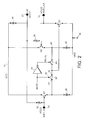
- FIG. 2 illustrates a circuit according to one embodiment of the invention which overcomes these two difficulties.
- the switching element in the circuit is denoted M1 and takes the form of an MOS transistor having a gate 20, a drain 22 and a source 24.
- the mute control signal MUTE is supplied to the gate 20.
- the audio input node is labelled 10 and the audio output node is labelled 12.
- the circuit of Figure 2 there is a voltage reduction component in the form of a bipolar transistor Q1 which has its base connected to the audio input node 10, its collector connected to the positive voltage supply rail 14 and its emitter connected via a current source 26 to the ground supply rail 16.
- the emitter of the bipolar transistor Q1 is also connected to the drain 22 of the mute control switch M1.
- the transistor Q1 has the effect of lowering the voltage level of the audio input signal via the base emitter voltage V be of the transistor Q1 such that the voltage level of the audio signal applied to the drain 22 of the mute control switch M1 is lowered by that amount. For a typical bipolar transistor this can lower the audio level by around 0.7V.
- the source of the mute control switch 24 is connected to a voltage raising component in the form of another bipolar transistor Q3.
- This bipolar transistor Q3 has its base connected to the source 24 of the mute control switch M1, its collector connected to the ground supply rail 16 and its emitter connected to the audio output node 12. It is of opposite polarity to the voltage reduction transistor Q1.
- This transistor accordingly lifts the level of the audio signal passed by the switch M1 via the base emitter voltage of the transistor Q3, which, of course, will be similar to the reduction which was introduced by the voltage reduction transistor Q1.
- the biasing voltage for biasing the audio signal at VCC/2 is illustrated as being input from a bias voltage node 30 where the bias voltage is labelled Vref and has a value of VCC/2. This is supplied via a resistor 32 to the audio input signal audio_in.
- Figure 2 further illustrates a current source 34 connected between the positive supply rail 14 and the audio output node 12, which acts to bias the transistor Q3.
- Figure 2 further illustrates circuit components which overcome the difficulty discussed earlier of the "pops and clicks" which can sometimes be heard due to the change in DC bias level when the mute control signal changes its status.
- These circuit components are a second MOS transistor labelled M2, a further bipolar transistor labelled Q2, a resistor 36, a current source 38 and an inverter 40. These circuit components are connected as follows.
- the inverter 40 is connected to receive the mute control signal MUTE and to supply an inverted version thereof to the gate of the transistor M2.
- the source/drain path of the transistor M2 is connected between the mute control switch M1 and a voltage node 42. That voltage node is held at a voltage level being VCC/2 -V beQ2 by virtue of the biasing arrangement introduced by the resistor 36 which is connected between the bias input voltage node 30 and the base of the bipolar transistor Q2.
- the emitter of the transistor Q2 is connected to the voltage node 42 while the collector of the transistor Q2 is connected to the positive voltage supply rail 14.
- the current source 38 is connected between the voltage node 42 and the ground supply rail 16.
- the circuit elements transistor Q2, resistor 36 and current source 38 to some extent mirror the circuit elements transistor Q1, current source 26 and resistor 32 on the input side of the circuit.
- the current source 38 biases the transistor Q2.
- MUTE an inverted version of the mute signal MUTE is supplied to the transistor M2, as M1 is made open circuit by the mute signal, M2 is closed.
- the transistor Q2 and the transistor M2 maintain the DC conditions at the base of the voltage raising transistor Q3 and hence at the output of the circuit.
- circuit of Figure 2 has two distinct advantages over the known circuit of Figure 1.
- a lower voltage level for the mute control signal MUTE is adequate, possibly of around 1.5V for a 1.8 voltage supply, due to the fact that the DC level of the audio input signal, audio_in is reduced prior to its application to the mute control switch.
- a further biasing arrangement is introduced to ensure that the DC conditions are maintained at the output node regardless of the status of the mute control switch. This avoids the irritating and possibly damaging "pops and click" which can occur when there is a change in the DC bias at the output node with a change in status of the mute control signal.
- Figure 3 illustrates a transistor implementation of the circuit of Figure 2. Like numerals denote like circuit elements as in Figure 2. The remaining circuit elements illustrated in Figure 3 are not discussed further herein because they do not form part of the invention but are illustrated in the Figure for the sake of completeness for one particular working implementation of the circuit.
Landscapes
- Amplifiers (AREA)
Abstract
Description
Claims (7)
- A mute switch comprising:a first switching element having a control gate for receiving a mute control signal and a controllable path for selectively supplying an audio signal from an input node to an output node;a voltage reduction component connected between said input node and the switching element for reducing the voltage level of the audio signal prior to its application to the input node; anda voltage raising component connected between the switching element and the output node for raising the voltage level of the audio signal prior to its application to the output node.
- A mute switch according to claim 1, wherein the switching element comprises a field effect transistor.
- A mute switch according to claim 1 or 2, wherein the voltage reduction component comprises a bipolar transistor having its base connected to said input node and its emitter connected to the switching element.
- A mute switch according to any preceding claim, wherein the voltage raising component comprises a bipolar transistor having its base connected to the switching element and its emitter connected to the output node.
- A mute switch according to claim 3 or claims 3 and 4, wherein a current source is connected between the emitter of the voltage reduction component and a voltage supply terminal.
- A mute switch according to any preceding claim, which comprises circuitry for maintaining a DC level of the audio signal regardless of the status of the mute control signal.
- A method of operating a mute control switch comprising the steps of:reducing the voltage level of an audio input signal prior to its application to a controllable path of the control switch;selectively switching the mute control switch using a mute control signal; andraising the voltage level of an audio signal passed by the mute control switch prior to applying said audio signal to an output node.
Priority Applications (3)
| Application Number | Priority Date | Filing Date | Title |
|---|---|---|---|
| DE60116572T DE60116572D1 (en) | 2001-05-15 | 2001-05-15 | mute switch |
| EP01304303A EP1258986B1 (en) | 2001-05-15 | 2001-05-15 | Mute switch |
| US10/147,436 US7187774B2 (en) | 2001-05-15 | 2002-05-15 | Mute switch |
Applications Claiming Priority (1)
| Application Number | Priority Date | Filing Date | Title |
|---|---|---|---|
| EP01304303A EP1258986B1 (en) | 2001-05-15 | 2001-05-15 | Mute switch |
Publications (2)
| Publication Number | Publication Date |
|---|---|
| EP1258986A1 true EP1258986A1 (en) | 2002-11-20 |
| EP1258986B1 EP1258986B1 (en) | 2006-01-11 |
Family
ID=8181966
Family Applications (1)
| Application Number | Title | Priority Date | Filing Date |
|---|---|---|---|
| EP01304303A Expired - Lifetime EP1258986B1 (en) | 2001-05-15 | 2001-05-15 | Mute switch |
Country Status (3)
| Country | Link |
|---|---|
| US (1) | US7187774B2 (en) |
| EP (1) | EP1258986B1 (en) |
| DE (1) | DE60116572D1 (en) |
Families Citing this family (7)
| Publication number | Priority date | Publication date | Assignee | Title |
|---|---|---|---|---|
| TWI230557B (en) * | 2003-11-06 | 2005-04-01 | Liteon It Corp | Mute circuit for use in the duration of power switching |
| US20060023896A1 (en) * | 2004-07-28 | 2006-02-02 | Ginsberg Mark G | Apparatus and method for controlling output signals from an amplifier when changing state |
| JP2006222758A (en) * | 2005-02-10 | 2006-08-24 | Orion Denki Kk | Electronic apparatus with voice mute control circuit |
| TWI327871B (en) * | 2006-01-05 | 2010-07-21 | Chunghwa Picture Tubes Ltd | Circuit for suppressing audio noise |
| US8218793B2 (en) * | 2006-12-11 | 2012-07-10 | Mediatek Inc. | Apparatus and muting circuit |
| USD964286S1 (en) * | 2020-04-10 | 2022-09-20 | Nathan Scott Murphy | Mute switch for instrument cables |
| TWI768466B (en) * | 2020-09-10 | 2022-06-21 | 美律實業股份有限公司 | Playback device and control method |
Citations (3)
| Publication number | Priority date | Publication date | Assignee | Title |
|---|---|---|---|---|
| US5300892A (en) * | 1991-09-11 | 1994-04-05 | Rohm Co., Ltd. | Audio signal amplifier circuit |
| US6016352A (en) * | 1997-11-20 | 2000-01-18 | Intel Corporation | Low distortion audio muting circuit |
| JP2001127569A (en) * | 1999-10-28 | 2001-05-11 | Kawasaki Steel Corp | Mute circuit |
Family Cites Families (3)
| Publication number | Priority date | Publication date | Assignee | Title |
|---|---|---|---|---|
| JP3002555B2 (en) * | 1991-03-18 | 2000-01-24 | 三菱電機株式会社 | Signal processing device |
| US5394476A (en) * | 1992-12-17 | 1995-02-28 | Motorola, Inc. | Volume control device |
| JP3398113B2 (en) * | 2000-02-14 | 2003-04-21 | ローム株式会社 | Mute circuit and digital audio amplifier circuit |
-
2001
- 2001-05-15 EP EP01304303A patent/EP1258986B1/en not_active Expired - Lifetime
- 2001-05-15 DE DE60116572T patent/DE60116572D1/en not_active Expired - Lifetime
-
2002
- 2002-05-15 US US10/147,436 patent/US7187774B2/en not_active Expired - Fee Related
Patent Citations (3)
| Publication number | Priority date | Publication date | Assignee | Title |
|---|---|---|---|---|
| US5300892A (en) * | 1991-09-11 | 1994-04-05 | Rohm Co., Ltd. | Audio signal amplifier circuit |
| US6016352A (en) * | 1997-11-20 | 2000-01-18 | Intel Corporation | Low distortion audio muting circuit |
| JP2001127569A (en) * | 1999-10-28 | 2001-05-11 | Kawasaki Steel Corp | Mute circuit |
Non-Patent Citations (1)
| Title |
|---|
| PATENT ABSTRACTS OF JAPAN vol. 2000, no. 22 9 March 2001 (2001-03-09) * |
Also Published As
| Publication number | Publication date |
|---|---|
| DE60116572D1 (en) | 2006-04-06 |
| EP1258986B1 (en) | 2006-01-11 |
| US20030016836A1 (en) | 2003-01-23 |
| US7187774B2 (en) | 2007-03-06 |
Similar Documents
| Publication | Publication Date | Title |
|---|---|---|
| US6661277B2 (en) | Enhanced conductivity body biased PMOS driver | |
| US4160934A (en) | Current control circuit for light emitting diode | |
| US7863951B2 (en) | Methods for adaptive trip point detection | |
| US7463066B1 (en) | Rail-to-rail source followers | |
| US6154085A (en) | Constant gate drive MOS analog switch | |
| US20080284405A1 (en) | Enhanced Cascode Performance By Reduced Impact Ionization | |
| US5252910A (en) | Current mirror operating under low voltage | |
| USRE41982E1 (en) | Circuitry to provide a low power input buffer | |
| US6104229A (en) | High voltage tolerable input buffer and method for operating same | |
| US5467050A (en) | Dynamic biasing circuit for semiconductor device | |
| KR100205506B1 (en) | Switchable current-reference voltage generator | |
| EP1258986B1 (en) | Mute switch | |
| US6388476B1 (en) | Self-switched cascode write driver | |
| KR20020067531A (en) | Bootstrapped dual-gate class e amplifier circuit | |
| US6624683B1 (en) | Threshold voltage reduction of a transistor connected as a diode | |
| US6985028B2 (en) | Programmable linear-in-dB or linear bias current source and methods to implement current reduction in a PA driver with built-in current steering VGA | |
| US6414533B1 (en) | Over-voltage tolerant, active pull-up clamp circuit for a CMOS crossbar switch | |
| US7005913B2 (en) | I/O buffer with wide range voltage translator | |
| US6031392A (en) | TTL input stage for negative supply systems | |
| US6614280B1 (en) | Voltage buffer for large gate loads with rail-to-rail operation and preferable use in LDO's | |
| US6362655B1 (en) | Linear active resistor and driver circuit incorporating the same | |
| US6275082B1 (en) | Receiver with switched current feedback for controlled hysteresis | |
| US6031417A (en) | Differential amplifier for multiple supply voltages and biasing device therefore | |
| KR100333240B1 (en) | Input amplifier with one-side interruption of current for input signals with steep edge | |
| KR19980081060A (en) | Input Amplifiers for Input Signals with Steep Edges |
Legal Events
| Date | Code | Title | Description |
|---|---|---|---|
| PUAI | Public reference made under article 153(3) epc to a published international application that has entered the european phase |
Free format text: ORIGINAL CODE: 0009012 |
|
| AK | Designated contracting states |
Kind code of ref document: A1 Designated state(s): AT BE CH CY DE DK ES FI FR GB GR IE IT LI LU MC NL PT SE TR |
|
| AX | Request for extension of the european patent |
Free format text: AL;LT;LV;MK;RO;SI |
|
| 17P | Request for examination filed |
Effective date: 20030513 |
|
| AKX | Designation fees paid |
Designated state(s): DE FR GB IT |
|
| 17Q | First examination report despatched |
Effective date: 20041111 |
|
| GRAP | Despatch of communication of intention to grant a patent |
Free format text: ORIGINAL CODE: EPIDOSNIGR1 |
|
| GRAS | Grant fee paid |
Free format text: ORIGINAL CODE: EPIDOSNIGR3 |
|
| GRAA | (expected) grant |
Free format text: ORIGINAL CODE: 0009210 |
|
| AK | Designated contracting states |
Kind code of ref document: B1 Designated state(s): DE FR GB IT |
|
| PG25 | Lapsed in a contracting state [announced via postgrant information from national office to epo] |
Ref country code: IT Free format text: LAPSE BECAUSE OF FAILURE TO SUBMIT A TRANSLATION OF THE DESCRIPTION OR TO PAY THE FEE WITHIN THE PRESCRIBED TIME-LIMIT;WARNING: LAPSES OF ITALIAN PATENTS WITH EFFECTIVE DATE BEFORE 2007 MAY HAVE OCCURRED AT ANY TIME BEFORE 2007. THE CORRECT EFFECTIVE DATE MAY BE DIFFERENT FROM THE ONE RECORDED. Effective date: 20060111 |
|
| REF | Corresponds to: |
Ref document number: 60116572 Country of ref document: DE Date of ref document: 20060406 Kind code of ref document: P |
|
| PG25 | Lapsed in a contracting state [announced via postgrant information from national office to epo] |
Ref country code: DE Free format text: LAPSE BECAUSE OF FAILURE TO SUBMIT A TRANSLATION OF THE DESCRIPTION OR TO PAY THE FEE WITHIN THE PRESCRIBED TIME-LIMIT Effective date: 20060412 |
|
| ET | Fr: translation filed | ||
| PLBE | No opposition filed within time limit |
Free format text: ORIGINAL CODE: 0009261 |
|
| STAA | Information on the status of an ep patent application or granted ep patent |
Free format text: STATUS: NO OPPOSITION FILED WITHIN TIME LIMIT |
|
| 26N | No opposition filed |
Effective date: 20061012 |
|
| PGFP | Annual fee paid to national office [announced via postgrant information from national office to epo] |
Ref country code: FR Payment date: 20080530 Year of fee payment: 8 |
|
| PGFP | Annual fee paid to national office [announced via postgrant information from national office to epo] |
Ref country code: GB Payment date: 20080424 Year of fee payment: 8 |
|
| GBPC | Gb: european patent ceased through non-payment of renewal fee |
Effective date: 20090515 |
|
| REG | Reference to a national code |
Ref country code: FR Ref legal event code: ST Effective date: 20100129 |
|
| PG25 | Lapsed in a contracting state [announced via postgrant information from national office to epo] |
Ref country code: FR Free format text: LAPSE BECAUSE OF NON-PAYMENT OF DUE FEES Effective date: 20090602 |
|
| PG25 | Lapsed in a contracting state [announced via postgrant information from national office to epo] |
Ref country code: GB Free format text: LAPSE BECAUSE OF NON-PAYMENT OF DUE FEES Effective date: 20090515 |