EP1258930A2 - Magnetic tunneling junction and fabrication method thereof - Google Patents
Magnetic tunneling junction and fabrication method thereof Download PDFInfo
- Publication number
- EP1258930A2 EP1258930A2 EP02253351A EP02253351A EP1258930A2 EP 1258930 A2 EP1258930 A2 EP 1258930A2 EP 02253351 A EP02253351 A EP 02253351A EP 02253351 A EP02253351 A EP 02253351A EP 1258930 A2 EP1258930 A2 EP 1258930A2
- Authority
- EP
- European Patent Office
- Prior art keywords
- magnetic
- layer
- tunnel junction
- magnetic layer
- magnetic tunnel
- Prior art date
- Legal status (The legal status is an assumption and is not a legal conclusion. Google has not performed a legal analysis and makes no representation as to the accuracy of the status listed.)
- Granted
Links
Images





Classifications
-
- H—ELECTRICITY
- H10—SEMICONDUCTOR DEVICES; ELECTRIC SOLID-STATE DEVICES NOT OTHERWISE PROVIDED FOR
- H10N—ELECTRIC SOLID-STATE DEVICES NOT OTHERWISE PROVIDED FOR
- H10N50/00—Galvanomagnetic devices
- H10N50/01—Manufacture or treatment
-
- G—PHYSICS
- G11—INFORMATION STORAGE
- G11B—INFORMATION STORAGE BASED ON RELATIVE MOVEMENT BETWEEN RECORD CARRIER AND TRANSDUCER
- G11B5/00—Recording by magnetisation or demagnetisation of a record carrier; Reproducing by magnetic means; Record carriers therefor
- G11B5/127—Structure or manufacture of heads, e.g. inductive
- G11B5/33—Structure or manufacture of flux-sensitive heads, i.e. for reproduction only; Combination of such heads with means for recording or erasing only
- G11B5/39—Structure or manufacture of flux-sensitive heads, i.e. for reproduction only; Combination of such heads with means for recording or erasing only using magneto-resistive devices or effects
-
- B—PERFORMING OPERATIONS; TRANSPORTING
- B82—NANOTECHNOLOGY
- B82Y—SPECIFIC USES OR APPLICATIONS OF NANOSTRUCTURES; MEASUREMENT OR ANALYSIS OF NANOSTRUCTURES; MANUFACTURE OR TREATMENT OF NANOSTRUCTURES
- B82Y25/00—Nanomagnetism, e.g. magnetoimpedance, anisotropic magnetoresistance, giant magnetoresistance or tunneling magnetoresistance
-
- B—PERFORMING OPERATIONS; TRANSPORTING
- B82—NANOTECHNOLOGY
- B82Y—SPECIFIC USES OR APPLICATIONS OF NANOSTRUCTURES; MEASUREMENT OR ANALYSIS OF NANOSTRUCTURES; MANUFACTURE OR TREATMENT OF NANOSTRUCTURES
- B82Y40/00—Manufacture or treatment of nanostructures
-
- H—ELECTRICITY
- H01—ELECTRIC ELEMENTS
- H01F—MAGNETS; INDUCTANCES; TRANSFORMERS; SELECTION OF MATERIALS FOR THEIR MAGNETIC PROPERTIES
- H01F41/00—Apparatus or processes specially adapted for manufacturing or assembling magnets, inductances or transformers; Apparatus or processes specially adapted for manufacturing materials characterised by their magnetic properties
- H01F41/14—Apparatus or processes specially adapted for manufacturing or assembling magnets, inductances or transformers; Apparatus or processes specially adapted for manufacturing materials characterised by their magnetic properties for applying magnetic films to substrates
- H01F41/30—Apparatus or processes specially adapted for manufacturing or assembling magnets, inductances or transformers; Apparatus or processes specially adapted for manufacturing materials characterised by their magnetic properties for applying magnetic films to substrates for applying nanostructures, e.g. by molecular beam epitaxy [MBE]
- H01F41/302—Apparatus or processes specially adapted for manufacturing or assembling magnets, inductances or transformers; Apparatus or processes specially adapted for manufacturing materials characterised by their magnetic properties for applying magnetic films to substrates for applying nanostructures, e.g. by molecular beam epitaxy [MBE] for applying spin-exchange-coupled multilayers, e.g. nanostructured superlattices
- H01F41/305—Apparatus or processes specially adapted for manufacturing or assembling magnets, inductances or transformers; Apparatus or processes specially adapted for manufacturing materials characterised by their magnetic properties for applying magnetic films to substrates for applying nanostructures, e.g. by molecular beam epitaxy [MBE] for applying spin-exchange-coupled multilayers, e.g. nanostructured superlattices applying the spacer or adjusting its interface, e.g. in order to enable particular effect different from exchange coupling
- H01F41/307—Apparatus or processes specially adapted for manufacturing or assembling magnets, inductances or transformers; Apparatus or processes specially adapted for manufacturing materials characterised by their magnetic properties for applying magnetic films to substrates for applying nanostructures, e.g. by molecular beam epitaxy [MBE] for applying spin-exchange-coupled multilayers, e.g. nanostructured superlattices applying the spacer or adjusting its interface, e.g. in order to enable particular effect different from exchange coupling insulating or semiconductive spacer
-
- Y—GENERAL TAGGING OF NEW TECHNOLOGICAL DEVELOPMENTS; GENERAL TAGGING OF CROSS-SECTIONAL TECHNOLOGIES SPANNING OVER SEVERAL SECTIONS OF THE IPC; TECHNICAL SUBJECTS COVERED BY FORMER USPC CROSS-REFERENCE ART COLLECTIONS [XRACs] AND DIGESTS
- Y10—TECHNICAL SUBJECTS COVERED BY FORMER USPC
- Y10T—TECHNICAL SUBJECTS COVERED BY FORMER US CLASSIFICATION
- Y10T29/00—Metal working
- Y10T29/49—Method of mechanical manufacture
- Y10T29/49002—Electrical device making
- Y10T29/4902—Electromagnet, transformer or inductor
- Y10T29/49021—Magnetic recording reproducing transducer [e.g., tape head, core, etc.]
- Y10T29/49032—Fabricating head structure or component thereof
- Y10T29/49036—Fabricating head structure or component thereof including measuring or testing
- Y10T29/49043—Depositing magnetic layer or coating
- Y10T29/49044—Plural magnetic deposition layers
Definitions
- the present invention relates to a magnetic tunneling junction and its fabrication method, and more particularly, to a magnetic tunneling junction with improved electro-magnetic characteristics and thermal stability through a rapid thermal annealing.
- a core technology of a magnetic tunnel junction is a development technology of a thin film material assuming excellent and stable magnetic resistance characteristics and an integrated process technology using the conventional semiconductor circuit and process.
- Tunneling magnetoresistance refers to a phenomenon that a tunneling current differs according to a relative magnetization direction of a ferromagnetic material in a junction with a structure of a ferromagnetic material/insulation material/ferromagnetic material structure.
- the magnetic resistance thin film assuming the tunnel magnetic resistance, that is, a magnetic tunnel junction is spotlighted as a thin film device that is the most suitable for a nonvolatile magnetic random access memory (MRAM) device having excellent characteristics as well as a magnetic field sensor of a magnetic disk drive.
- MRAM nonvolatile magnetic random access memory
- Figure 1 is a sectional view of the magnetic tunnel junction, which includes: a substrate 11; a bottom lead 12; a seed layer 13; an anti-ferromagnetic layer 14; a first magnetic layer 15; a tunnel barrier layer 16; a second magnetic layer 17; and a top lead 18.
- the magnetic tunnel junction has a sandwich structure of the two first and second magnetic layers with the tunnel barrier 16 made as an insulation layer or an oxide layer (generally Al 2 O 3 ) interposed there between.
- the anti-ferromagnetic layer 14 is made of FeMn, IrMn or PtMn, or NiO.
- a current flows vertically to the layers, unlike a CIP (current in plane) type giant magnetoresistance (GMR) that flows in parallel to each layer.
- CIP current in plane
- GMR giant magnetoresistance
- the current in the magnetic tunnel junction (referred to as a 'tunneling current', hereinafter) is dependent on the relative magnetization direction of the two magnetic layers 15 and 17.
- Whether a corresponding bit is '0' or '1' can be discriminated by using the quality that the tunneling current differs (that is, a resistance value of the device differs) according to the direction of the spin.
- a bit can be written or read by applying a magnetic field to the magnetic tunnel junction.
- the magnetic tunnel junction includes a pseudo spin-valve type in which the direction of spin can be controlled by using two magnetic layers with different coercive forces and an exchange bias type in which one of two magnetic layers is fixed through an exchange biasing field of the anti-ferromagnetic layer to thereby control a spin direction of a different magnetic layer.
- the anti-ferromagnetic layer 14 is made of a synthetic anti-ferromagnetic material (ferromagnetic layer/non-magnetic layer/ferromagnetic layer) to increase the effect of fixing the first magnetic layer 15.
- TMR ratio is a critical factor having much influence on a density and a velocity of an MRAM device.
- the main reason for this is estimated to be a complicate magnetic switching behavior due to complicate magnetic domains and an unevenness of an infinitesimally patterned cell that is fabricated by an etching process.
- the magnetic tunnel junction is thermally treated for a long time while applying a magnetic field thereto, so as to improve the TMR ratio and the exchanging magnetic anisotropy: H ex ) of the magnetic tunnel junction and to increase the squareness of the free layer hysteresis loop.
- an aim of the present invention is to improve a TMR ratio and an exchanging magnetic anisotropy (H ex ) of a magnetic tunnel function device only by a thermal treatment for a short time.
- Another aim of the present invention is to improve squareness in a magnetic switching of a free layer.
- Still another aim of the present invention is to improve a thermal stability of a magnetic tunnel junction.
- a fabrication method of a magnetic tunnel junction including the steps of: forming a magnetic tunnel junction constructed having a first magnetic layer, a tunnel barrier formed at an upper surface of the first magnetic layer and a second magnetic layer formed at an upper surface of the tunnel barrier; and thermally treating the junction rapidly for 5 seconds ⁇ 10 minutes at a temperature of 200 ⁇ 600°C to re-distribute atoms in the tunnel barrier and make the interface between the tunnel barrier and the magnetic layer to be even.
- the rapid thermal annealing can be made while applying a magnetic field, and preferably, it is performed radially by using an infrared lamp.
- a thermal treatment can be additionally performed in the same manner as in the conventional thermal treatment, after the rapid thermal annealing.
- the present invention accomplishes an economic effect by considerably reducing time taken for a thermal treatment and a cooling time, and improved electro-magnetic characteristics and thermal stability.
- a magnetic tunnel junction fabricated by the present invention can have an exchange bias type, in which a first magnetic layer is a pinned layer, a second magnetic layer is a free layer, and an anti-ferromagnetic layer, a pinning layer for pinning a spin direction of the first magnetic layer, is formed at the other side of the first magnetic layer.
- the first and the second magnetic layers can have a pseudo spin-valve type with different coercive forces to control the spin direction.
- the rapid thermal annealing adopted in the present invention is the radial thermal treatment using the infrared lamp, for a quick heating and cooling.
- the RTA has the total treatment time of less than 2 minutes and electro-magnetically and thermally optimize the characteristics of the magnetic tunnel junction much faster than the CTA.
- Figure 2 is a graph showing the variation of TMR ratio and exchange bias field (H ex ) against annealing temperature for a magnetic tunnel junction thermally treated by a CTA and an RTA.
- the TMR ratio is continuously increased up to 40% as the temperature goes up to 230°C. It is attributable to oxygen redistribution and homogenization in the Al oxide barrier during annealing process, giving rise to the improvement in the properties of MTJs.
- the exchange bias field (Hex) of the CTA is increased from 180 Oe to 230 Oe up to a temperature of 230°C and then sharply decreased thereafter.
- the highest value of 230 Oe is shown at a temperature range of 250 ⁇ 400°C and then very slowly decreased thereafter as the temperature is increased.
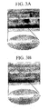
- Figure 3A is a sectional view showing a magnetic tunnel junction before applying a rapid thermal annealing method of the present invention.
- the Al oxide layer, the tunnel barrier of the magnetic tunnel junction before a thermal treatment exhibits irregular interface with respect to the upper and lower magnetic layers and not clearly shown.
- Figure 3B is a section view of the magnetic tunnel junction after applying the rapid thermal annealing method of the present invention.
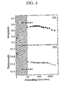
- Figure 4 is graph showing the variation of the effective barrier thickness and height of a tunnel barrier in a magnetic tunnel junction after applying the rapid thermal annealing method of the present invention.
- the graph of Figure 4 was obtained by analyzing a current-voltage curve from Simmons model at a temperature of 300°C.
- the effective barrier thickness and the height of the oxide layer is rapidly changed within the initial 10 seconds of the RTA process.
- a change in the oxide layer after the initial 10 seconds is very slowly made according to the thermal treatment time.
- Figure 5 is a graph showing the variation of TMR curves and M-H loops of a magnetic tunnel junction (a) before thermal treatment, a magnetic tunnel junction (b) thermally treated by the CTA at a temperature of 300°C, and a magnetic tunnel junction (c) which was thermally treated with the RTA at a temperature of 300°C and then thermally treated again by the CTA at a temperature of 300°C.
- Figure 5C shows much improved TMR ratio and exchange bias field compared with Figure 5B.
- the magnetic tunnel junction (C) which has undergone the RTA and the CTA is similar to the magnetic moment of the magnetic tunnel junction (a) which has not been subjected to the thermal treatment.
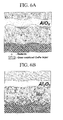
- Figures 6A through 6C are schematic views showing a distribution of Mn ion of a magnetic tunnel junction (6A) before thermal treatment, a magnetic tunnel junction (6B) thermally treated by the CTA at 300°C, and a magnetic tunnel junction (6C) which was thermally treated with the RTA at 300°C and then thermally treated again by the CTA at 300°C.
- the improvement of the tunneling effect by the RTA owes to the fact that the oxygen is re-distributed and even by the RTA in the over-oxidized tunnel barrier (AlO x ).
- Mn of the anti-ferromagnetic layer (FeMn) easily diffuses into the tunnel barrier through point defects or grain boundaries existing in the pinned layer to make a crucial influence on the tunneling magnetoresistance of the magnetic tunnel junction.
- Figures 7A through 7D are graphs of Auger electron spectroscopy of a magnetic tunnel junction (7A) before thermal treatment, a magnetic tunnel junction (7B) thermally treated by the CTA at 300°C, a magnetic tunnel junction (7C) thermally treated with the RTA at 300°C, and a magnetic tunnel junction (7D) which was thermally treated with the RTA at 300°C and then thermally treated again by the CTA at 300°C.
- the Auger electron spectroscopy analysis directly exhibits the thermal stability improvement by the RTA.
- the magnetic tunneling junction and its fabrication method of the present invention has many advantages.
- the TMR ratio of the magnetic tunnel junction is considerably improved.
- the characteristics of the magnetic tunnel junction can be optimized more quickly and effectively compared to the conventional thermal treatment method.
- the tunneling effect is improved by reducing the irregularity of the oxide layer, the tunnel barrier.
- the effect of the thermal treatment affecting the oxide layer is made very quickly, so that the oxide layer can be optimized effectively.
- the TMR ratio and the exchange bias field can be remarkably improved.
Landscapes
- Engineering & Computer Science (AREA)
- Chemical & Material Sciences (AREA)
- Nanotechnology (AREA)
- Crystallography & Structural Chemistry (AREA)
- Manufacturing & Machinery (AREA)
- Physics & Mathematics (AREA)
- Power Engineering (AREA)
- Spectroscopy & Molecular Physics (AREA)
- Condensed Matter Physics & Semiconductors (AREA)
- General Physics & Mathematics (AREA)
- Hall/Mr Elements (AREA)
- Magnetic Heads (AREA)
- Mram Or Spin Memory Techniques (AREA)
Abstract
Description
| CTA | RTA | |
| | 15 | 10 seconds |
| Thermal annealing time | One | 10 seconds |
| Cooling time | Within 1.5 hour | Within 1 minute and 30 seconds |
| Total treatment time | More than 2.5 hours | Within 2 |
| Treatment temperature | ||
| 200∼300° | 200∼400°C |
Claims (12)
- A fabrication method of a magnet tunnel junction comprising the steps of:forming a magnetic tunnel junction constructed having a first magnetic layer, a tunnel barrier formed at an upper surface of the first magnetic layer and a second magnetic layer formed at an upper surface of the tunnel barrier; andthermally treating the junction rapidly for 5 seconds ∼10 minutes at a temperature of 200∼600°C to re-distribute atoms in the tunnel barrier and make the interface between the tunnel barrier and the magnetic layer to be even.
- The method of claim 1, wherein the rapid thermal annealing is performed by applying a magnetic field.
- The method of claim 1, wherein the rapid thermal annealing Is radially performed by using an infrared lamp.
- The method of claim 1, wherein, after the rapid thermal annealing, a cooling operation is performed for 10 seconds ∼ 10 minutes.
- The method of claim 1, wherein the rapid thermal annealing is performed in a temperature range of 250 ∼ 400°.
- The method of claim 1, wherein, after the rapid thermal annealing, a thermal treatment is additionally performed.
- The method of claim 1, wherein a first magnetic layer is a pinned layer, a second magnetic layer is a free layer, and an anti-ferromagnetic layer, a pinning layer for pinning a spin direction of the first magnetic layer, is formed at the other side of the first magnetic layer.
- The method of claim 7, wherein the anti-ferromagnetic layer is made of one selected from the group consisting of FeMn, IrMn, PtMn or NiO.
- The method of claim 8, wherein, in case of FeMn, thermal treatment is performed in a temperature range of 200 ∼ 400°C, and in case of IrMn or PtMn, a thermal treatment is performed in the temperature range of 300 ∼ 600°C.
- The method of claim 7, wherein the anti-ferromagnetic layer is a synthetic anti-ferromagnetic material constructed by ferromagnetic layer/non-magnetic layer/ferromagnetic layer.
- The method of claim 1, wherein the first magnetic layer and the second magnetic layer have different coercive forces to control the spin direction.
- A magnetic tunnel junction fabricated by the method of claim 1.
Applications Claiming Priority (2)
| Application Number | Priority Date | Filing Date | Title |
|---|---|---|---|
| KR2001026486 | 2001-05-15 | ||
| KR10-2001-0026486A KR100407907B1 (en) | 2001-05-15 | 2001-05-15 | Thermal anneal method of magnetic tunnel junction, and magnetic tunneling junction fabricated by the method |
Publications (3)
| Publication Number | Publication Date |
|---|---|
| EP1258930A2 true EP1258930A2 (en) | 2002-11-20 |
| EP1258930A3 EP1258930A3 (en) | 2005-11-16 |
| EP1258930B1 EP1258930B1 (en) | 2007-10-17 |
Family
ID=19709492
Family Applications (1)
| Application Number | Title | Priority Date | Filing Date |
|---|---|---|---|
| EP02253351A Expired - Lifetime EP1258930B1 (en) | 2001-05-15 | 2002-05-14 | Fabrication method for a magnetic tunneling junction |
Country Status (6)
| Country | Link |
|---|---|
| US (1) | US6848169B2 (en) |
| EP (1) | EP1258930B1 (en) |
| JP (1) | JP4498660B2 (en) |
| KR (1) | KR100407907B1 (en) |
| AT (1) | ATE376259T1 (en) |
| DE (1) | DE60222963T2 (en) |
Cited By (1)
| Publication number | Priority date | Publication date | Assignee | Title |
|---|---|---|---|---|
| CN102832336A (en) * | 2012-08-28 | 2012-12-19 | 淮阴工学院 | Method for improving exchange bias field heat stability of ferromagnetic/antiferromagnetic dual-layer membrane by laser annealing |
Families Citing this family (30)
| Publication number | Priority date | Publication date | Assignee | Title |
|---|---|---|---|---|
| JP2004079632A (en) * | 2002-08-12 | 2004-03-11 | Toshiba Corp | Semiconductor integrated circuit device |
| KR20040083934A (en) * | 2003-03-25 | 2004-10-06 | 주식회사 하이닉스반도체 | A method for manufacturing of a Magnetic random access memory |
| US7054085B2 (en) * | 2003-06-30 | 2006-05-30 | Hitachi Global Storage Technologies Netherlands B.V. | Use of shunt resistor with large RA product tunnel barriers |
| JP2006059963A (en) * | 2004-08-19 | 2006-03-02 | Tohoku Univ | Tunnel-type magnetoresistive element, method for manufacturing the same, and apparatus for manufacturing the same |
| JP4101240B2 (en) * | 2005-01-28 | 2008-06-18 | Tdk株式会社 | Magnetic head |
| US7695761B1 (en) | 2006-12-21 | 2010-04-13 | Western Digital (Fremont), Llc | Method and system for providing a spin tunneling magnetic element having a crystalline barrier layer |
| US8559141B1 (en) | 2007-05-07 | 2013-10-15 | Western Digital (Fremont), Llc | Spin tunneling magnetic element promoting free layer crystal growth from a barrier layer interface |
| US8545999B1 (en) | 2008-02-21 | 2013-10-01 | Western Digital (Fremont), Llc | Method and system for providing a magnetoresistive structure |
| US8381391B2 (en) * | 2009-06-26 | 2013-02-26 | Western Digital (Fremont), Llc | Method for providing a magnetic recording transducer |
| US8498084B1 (en) | 2009-07-21 | 2013-07-30 | Western Digital (Fremont), Llc | Magnetoresistive sensors having an improved free layer |
| US8194365B1 (en) | 2009-09-03 | 2012-06-05 | Western Digital (Fremont), Llc | Method and system for providing a read sensor having a low magnetostriction free layer |
| US8336194B2 (en) * | 2009-11-03 | 2012-12-25 | Western Digital (Fremont), Llc | Method of fabricating a tunneling magnetoresistive (TMR) reader |
| US9054298B2 (en) * | 2010-12-10 | 2015-06-09 | Avalanche Technology, Inc. | Magnetic random access memory (MRAM) with enhanced magnetic stiffness and method of making same |
| US8760819B1 (en) | 2010-12-23 | 2014-06-24 | Western Digital (Fremont), Llc | Magnetic recording sensor with sputtered antiferromagnetic coupling trilayer between plated ferromagnetic shields |
| US9880232B2 (en) * | 2012-03-14 | 2018-01-30 | Seagate Technology Llc | Magnetic sensor manufacturing |
| US8797692B1 (en) | 2012-09-07 | 2014-08-05 | Western Digital (Fremont), Llc | Magnetic recording sensor with AFM exchange coupled shield stabilization |
| US9064534B1 (en) | 2012-11-30 | 2015-06-23 | Western Digital (Fremont), Llc | Process for providing a magnetic recording transducer with enhanced pinning layer stability |
| TWI501224B (en) * | 2013-03-07 | 2015-09-21 | Nat Univ Tsing Hua | Magnetic electronic device and manufacturing method thereof |
| US8780505B1 (en) | 2013-03-12 | 2014-07-15 | Western Digital (Fremont), Llc | Method and system for providing a read transducer having an improved composite magnetic shield |
| US9013836B1 (en) | 2013-04-02 | 2015-04-21 | Western Digital (Fremont), Llc | Method and system for providing an antiferromagnetically coupled return pole |
| US9070381B1 (en) | 2013-04-12 | 2015-06-30 | Western Digital (Fremont), Llc | Magnetic recording read transducer having a laminated free layer |
| US9431047B1 (en) | 2013-05-01 | 2016-08-30 | Western Digital (Fremont), Llc | Method for providing an improved AFM reader shield |
| US9361913B1 (en) | 2013-06-03 | 2016-06-07 | Western Digital (Fremont), Llc | Recording read heads with a multi-layer AFM layer methods and apparatuses |
| US9287494B1 (en) | 2013-06-28 | 2016-03-15 | Western Digital (Fremont), Llc | Magnetic tunnel junction (MTJ) with a magnesium oxide tunnel barrier |
| US9076954B2 (en) | 2013-08-08 | 2015-07-07 | Samsung Electronics Co., Ltd. | Method and system for providing magnetic memories switchable using spin accumulation and selectable using magnetoelectric devices |
| US9147408B1 (en) | 2013-12-19 | 2015-09-29 | Western Digital (Fremont), Llc | Heated AFM layer deposition and cooling process for TMR magnetic recording sensor with high pinning field |
| KR20160056376A (en) * | 2014-11-10 | 2016-05-20 | 삼성전자주식회사 | Method of forming metal oxide layer and magnetic memory device including the same |
| US10074387B1 (en) | 2014-12-21 | 2018-09-11 | Western Digital (Fremont), Llc | Method and system for providing a read transducer having symmetric antiferromagnetically coupled shields |
| CN105280809B (en) * | 2015-09-14 | 2018-03-27 | 华中科技大学 | A kind of magnetic tunnel-junction and preparation method thereof |
| US10622406B2 (en) * | 2018-07-03 | 2020-04-14 | International Business Machines Corporation | Dual metal nitride landing pad for MRAM devices |
Family Cites Families (10)
| Publication number | Priority date | Publication date | Assignee | Title |
|---|---|---|---|---|
| US5640343A (en) * | 1996-03-18 | 1997-06-17 | International Business Machines Corporation | Magnetic memory array using magnetic tunnel junction devices in the memory cells |
| KR100262282B1 (en) * | 1996-04-30 | 2000-10-02 | 니시무로 타이죠 | Magnetoresistive effect element |
| US5729410A (en) * | 1996-11-27 | 1998-03-17 | International Business Machines Corporation | Magnetic tunnel junction device with longitudinal biasing |
| US6391658B1 (en) * | 1999-10-26 | 2002-05-21 | International Business Machines Corporation | Formation of arrays of microelectronic elements |
| US6359289B1 (en) * | 2000-04-19 | 2002-03-19 | International Business Machines Corporation | Magnetic tunnel junction device with improved insulating tunnel barrier |
| JP4693292B2 (en) * | 2000-09-11 | 2011-06-01 | 株式会社東芝 | Ferromagnetic tunnel junction device and manufacturing method thereof |
| US20020131215A1 (en) * | 2001-03-14 | 2002-09-19 | Beach Robert S. | Tunnel junction and charge perpendicular-to-plane magnetic recording sensors and method of manufacture |
| US6649423B2 (en) * | 2001-10-04 | 2003-11-18 | Hewlett-Packard Development Company, L.P. | Method for modifying switching field characteristics of magnetic tunnel junctions |
| US6518588B1 (en) * | 2001-10-17 | 2003-02-11 | International Business Machines Corporation | Magnetic random access memory with thermally stable magnetic tunnel junction cells |
| US6822838B2 (en) * | 2002-04-02 | 2004-11-23 | International Business Machines Corporation | Dual magnetic tunnel junction sensor with a longitudinal bias stack |
-
2001
- 2001-05-15 KR KR10-2001-0026486A patent/KR100407907B1/en not_active Expired - Lifetime
-
2002
- 2002-05-13 US US10/145,167 patent/US6848169B2/en not_active Expired - Lifetime
- 2002-05-14 EP EP02253351A patent/EP1258930B1/en not_active Expired - Lifetime
- 2002-05-14 AT AT02253351T patent/ATE376259T1/en not_active IP Right Cessation
- 2002-05-14 DE DE60222963T patent/DE60222963T2/en not_active Expired - Lifetime
- 2002-05-15 JP JP2002140511A patent/JP4498660B2/en not_active Expired - Fee Related
Cited By (1)
| Publication number | Priority date | Publication date | Assignee | Title |
|---|---|---|---|---|
| CN102832336A (en) * | 2012-08-28 | 2012-12-19 | 淮阴工学院 | Method for improving exchange bias field heat stability of ferromagnetic/antiferromagnetic dual-layer membrane by laser annealing |
Also Published As
| Publication number | Publication date |
|---|---|
| US20020185196A1 (en) | 2002-12-12 |
| JP2003069113A (en) | 2003-03-07 |
| KR100407907B1 (en) | 2003-12-03 |
| DE60222963T2 (en) | 2008-07-31 |
| JP4498660B2 (en) | 2010-07-07 |
| US6848169B2 (en) | 2005-02-01 |
| ATE376259T1 (en) | 2007-11-15 |
| EP1258930A3 (en) | 2005-11-16 |
| KR20020087640A (en) | 2002-11-23 |
| DE60222963D1 (en) | 2007-11-29 |
| EP1258930B1 (en) | 2007-10-17 |
Similar Documents
| Publication | Publication Date | Title |
|---|---|---|
| US6848169B2 (en) | Magnetic tunneling junction and fabrication method thereof | |
| US7276384B2 (en) | Magnetic tunnel junctions with improved tunneling magneto-resistance | |
| US7160738B2 (en) | Magnetic annealing sequences for patterned MRAM synthetic antiferromagnetic pinned layers | |
| US7026671B2 (en) | Magnetoresistive effect element, magnetic memory device and manufacturing method of magnetoresistive effect element and magnetic memory device | |
| US7149105B2 (en) | Magnetic tunnel junctions for MRAM devices | |
| US7807218B2 (en) | High performance magnetic tunnel barriers with amorphous materials | |
| US7351483B2 (en) | Magnetic tunnel junctions using amorphous materials as reference and free layers | |
| US8736004B2 (en) | Magnetic tunnel junction for MRAM applications | |
| US8884389B2 (en) | Magnetoresistive element and method of manufacturing the same | |
| US20130037862A1 (en) | Magnetic random access memory | |
| US7616475B2 (en) | Memory element and memory | |
| JP2011198809A (en) | Magnetoresistive element, method for manufacturing the same, and magnetic memory | |
| US6649423B2 (en) | Method for modifying switching field characteristics of magnetic tunnel junctions | |
| US20090121266A1 (en) | Methods and structures for exchange-coupled magnetic multi-layer structure with improved operating temperature behavior | |
| US6960397B2 (en) | Magnetoresistance device | |
| KR100543265B1 (en) | Tunneling magnetoresistive element and manufacturing method thereof |
Legal Events
| Date | Code | Title | Description |
|---|---|---|---|
| PUAI | Public reference made under article 153(3) epc to a published international application that has entered the european phase |
Free format text: ORIGINAL CODE: 0009012 |
|
| 17P | Request for examination filed |
Effective date: 20020531 |
|
| AK | Designated contracting states |
Kind code of ref document: A2 Designated state(s): AT BE CH CY DE DK ES FI FR GB GR IE IT LI LU MC NL PT SE TR |
|
| AX | Request for extension of the european patent |
Free format text: AL;LT;LV;MK;RO;SI |
|
| RIN1 | Information on inventor provided before grant (corrected) |
Inventor name: HA, JAE-GEUN Inventor name: LEE, KYUNG-IL Inventor name: PARK, YOUNG-JOON Inventor name: LEE, WOO-YOUNG Inventor name: SHIN, KYUNG-HO,PATENT MANAGEMENT TEAM, KORCA INST. |
|
| PUAL | Search report despatched |
Free format text: ORIGINAL CODE: 0009013 |
|
| AK | Designated contracting states |
Kind code of ref document: A3 Designated state(s): AT BE CH CY DE DK ES FI FR GB GR IE IT LI LU MC NL PT SE TR |
|
| AX | Request for extension of the european patent |
Extension state: AL LT LV MK RO SI |
|
| AKX | Designation fees paid |
Designated state(s): AT BE CH CY DE DK ES FI FR GB GR IE IT LI LU MC NL PT SE TR |
|
| GRAP | Despatch of communication of intention to grant a patent |
Free format text: ORIGINAL CODE: EPIDOSNIGR1 |
|
| RIC1 | Information provided on ipc code assigned before grant |
Ipc: H01F 41/30 20060101ALN20070327BHEP Ipc: H01L 43/12 20060101AFI20070327BHEP |
|
| RTI1 | Title (correction) |
Free format text: FABRICATION METHOD FOR A MAGNETIC TUNNELING JUNCTION |
|
| RIN1 | Information on inventor provided before grant (corrected) |
Inventor name: LEE, WOO-YOUNG Inventor name: HA, JAE-GEUN Inventor name: PARK, YOUNG-JOON Inventor name: LEE, KYUNG-IL Inventor name: SHIN, KYUNG-HO,PATENT MANAGEMENT TEAM, KOREA INST. |
|
| GRAS | Grant fee paid |
Free format text: ORIGINAL CODE: EPIDOSNIGR3 |
|
| GRAA | (expected) grant |
Free format text: ORIGINAL CODE: 0009210 |
|
| AK | Designated contracting states |
Kind code of ref document: B1 Designated state(s): AT BE CH CY DE DK ES FI FR GB GR IE IT LI LU MC NL PT SE TR |
|
| REG | Reference to a national code |
Ref country code: GB Ref legal event code: FG4D |
|
| RIN1 | Information on inventor provided before grant (corrected) |
Inventor name: HA, JAE-GEUN Inventor name: LEE, KYUNG-IL Inventor name: LEE, WOO-YOUNG Inventor name: PARK, YOUNG-JOON Inventor name: SHIN, KYUNG-HO,PAT. MANGMT. TEAM, INST. OF SCIENCE |
|
| REG | Reference to a national code |
Ref country code: CH Ref legal event code: EP |
|
| REG | Reference to a national code |
Ref country code: IE Ref legal event code: FG4D |
|
| REF | Corresponds to: |
Ref document number: 60222963 Country of ref document: DE Date of ref document: 20071129 Kind code of ref document: P |
|
| ET | Fr: translation filed | ||
| NLV1 | Nl: lapsed or annulled due to failure to fulfill the requirements of art. 29p and 29m of the patents act | ||
| PG25 | Lapsed in a contracting state [announced via postgrant information from national office to epo] |
Ref country code: SE Free format text: LAPSE BECAUSE OF FAILURE TO SUBMIT A TRANSLATION OF THE DESCRIPTION OR TO PAY THE FEE WITHIN THE PRESCRIBED TIME-LIMIT Effective date: 20080117 Ref country code: CH Free format text: LAPSE BECAUSE OF FAILURE TO SUBMIT A TRANSLATION OF THE DESCRIPTION OR TO PAY THE FEE WITHIN THE PRESCRIBED TIME-LIMIT Effective date: 20071017 Ref country code: ES Free format text: LAPSE BECAUSE OF FAILURE TO SUBMIT A TRANSLATION OF THE DESCRIPTION OR TO PAY THE FEE WITHIN THE PRESCRIBED TIME-LIMIT Effective date: 20080128 Ref country code: LI Free format text: LAPSE BECAUSE OF FAILURE TO SUBMIT A TRANSLATION OF THE DESCRIPTION OR TO PAY THE FEE WITHIN THE PRESCRIBED TIME-LIMIT Effective date: 20071017 Ref country code: NL Free format text: LAPSE BECAUSE OF FAILURE TO SUBMIT A TRANSLATION OF THE DESCRIPTION OR TO PAY THE FEE WITHIN THE PRESCRIBED TIME-LIMIT Effective date: 20071017 |
|
| REG | Reference to a national code |
Ref country code: CH Ref legal event code: PL |
|
| PG25 | Lapsed in a contracting state [announced via postgrant information from national office to epo] |
Ref country code: PT Free format text: LAPSE BECAUSE OF FAILURE TO SUBMIT A TRANSLATION OF THE DESCRIPTION OR TO PAY THE FEE WITHIN THE PRESCRIBED TIME-LIMIT Effective date: 20080317 |
|
| PG25 | Lapsed in a contracting state [announced via postgrant information from national office to epo] |
Ref country code: AT Free format text: LAPSE BECAUSE OF FAILURE TO SUBMIT A TRANSLATION OF THE DESCRIPTION OR TO PAY THE FEE WITHIN THE PRESCRIBED TIME-LIMIT Effective date: 20071017 |
|
| PG25 | Lapsed in a contracting state [announced via postgrant information from national office to epo] |
Ref country code: DK Free format text: LAPSE BECAUSE OF FAILURE TO SUBMIT A TRANSLATION OF THE DESCRIPTION OR TO PAY THE FEE WITHIN THE PRESCRIBED TIME-LIMIT Effective date: 20071017 |
|
| PLBE | No opposition filed within time limit |
Free format text: ORIGINAL CODE: 0009261 |
|
| STAA | Information on the status of an ep patent application or granted ep patent |
Free format text: STATUS: NO OPPOSITION FILED WITHIN TIME LIMIT |
|
| PG25 | Lapsed in a contracting state [announced via postgrant information from national office to epo] |
Ref country code: BE Free format text: LAPSE BECAUSE OF FAILURE TO SUBMIT A TRANSLATION OF THE DESCRIPTION OR TO PAY THE FEE WITHIN THE PRESCRIBED TIME-LIMIT Effective date: 20071017 |
|
| 26N | No opposition filed |
Effective date: 20080718 |
|
| PG25 | Lapsed in a contracting state [announced via postgrant information from national office to epo] |
Ref country code: MC Free format text: LAPSE BECAUSE OF NON-PAYMENT OF DUE FEES Effective date: 20080531 |
|
| PG25 | Lapsed in a contracting state [announced via postgrant information from national office to epo] |
Ref country code: GR Free format text: LAPSE BECAUSE OF FAILURE TO SUBMIT A TRANSLATION OF THE DESCRIPTION OR TO PAY THE FEE WITHIN THE PRESCRIBED TIME-LIMIT Effective date: 20080118 |
|
| PG25 | Lapsed in a contracting state [announced via postgrant information from national office to epo] |
Ref country code: FI Free format text: LAPSE BECAUSE OF FAILURE TO SUBMIT A TRANSLATION OF THE DESCRIPTION OR TO PAY THE FEE WITHIN THE PRESCRIBED TIME-LIMIT Effective date: 20071017 |
|
| PG25 | Lapsed in a contracting state [announced via postgrant information from national office to epo] |
Ref country code: IE Free format text: LAPSE BECAUSE OF NON-PAYMENT OF DUE FEES Effective date: 20080514 |
|
| PG25 | Lapsed in a contracting state [announced via postgrant information from national office to epo] |
Ref country code: CY Free format text: LAPSE BECAUSE OF FAILURE TO SUBMIT A TRANSLATION OF THE DESCRIPTION OR TO PAY THE FEE WITHIN THE PRESCRIBED TIME-LIMIT Effective date: 20071017 |
|
| PG25 | Lapsed in a contracting state [announced via postgrant information from national office to epo] |
Ref country code: LU Free format text: LAPSE BECAUSE OF NON-PAYMENT OF DUE FEES Effective date: 20080514 |
|
| PG25 | Lapsed in a contracting state [announced via postgrant information from national office to epo] |
Ref country code: TR Free format text: LAPSE BECAUSE OF FAILURE TO SUBMIT A TRANSLATION OF THE DESCRIPTION OR TO PAY THE FEE WITHIN THE PRESCRIBED TIME-LIMIT Effective date: 20071017 |
|
| REG | Reference to a national code |
Ref country code: FR Ref legal event code: PLFP Year of fee payment: 15 |
|
| PGFP | Annual fee paid to national office [announced via postgrant information from national office to epo] |
Ref country code: DE Payment date: 20160511 Year of fee payment: 15 Ref country code: GB Payment date: 20160511 Year of fee payment: 15 |
|
| PGFP | Annual fee paid to national office [announced via postgrant information from national office to epo] |
Ref country code: FR Payment date: 20160512 Year of fee payment: 15 Ref country code: IT Payment date: 20160512 Year of fee payment: 15 |
|
| REG | Reference to a national code |
Ref country code: DE Ref legal event code: R119 Ref document number: 60222963 Country of ref document: DE |
|
| GBPC | Gb: european patent ceased through non-payment of renewal fee |
Effective date: 20170514 |
|
| REG | Reference to a national code |
Ref country code: FR Ref legal event code: ST Effective date: 20180131 |
|
| PG25 | Lapsed in a contracting state [announced via postgrant information from national office to epo] |
Ref country code: GB Free format text: LAPSE BECAUSE OF NON-PAYMENT OF DUE FEES Effective date: 20170514 Ref country code: DE Free format text: LAPSE BECAUSE OF NON-PAYMENT OF DUE FEES Effective date: 20171201 |
|
| PG25 | Lapsed in a contracting state [announced via postgrant information from national office to epo] |
Ref country code: FR Free format text: LAPSE BECAUSE OF NON-PAYMENT OF DUE FEES Effective date: 20170531 Ref country code: IT Free format text: LAPSE BECAUSE OF NON-PAYMENT OF DUE FEES Effective date: 20170514 |