EP1258922A2 - Organic electroluminescent display with integrated resistive touch screen - Google Patents
Organic electroluminescent display with integrated resistive touch screen Download PDFInfo
- Publication number
- EP1258922A2 EP1258922A2 EP02076758A EP02076758A EP1258922A2 EP 1258922 A2 EP1258922 A2 EP 1258922A2 EP 02076758 A EP02076758 A EP 02076758A EP 02076758 A EP02076758 A EP 02076758A EP 1258922 A2 EP1258922 A2 EP 1258922A2
- Authority
- EP
- European Patent Office
- Prior art keywords
- touch screen
- display
- substrate
- circuit
- touch
- Prior art date
- Legal status (The legal status is an assumption and is not a legal conclusion. Google has not performed a legal analysis and makes no representation as to the accuracy of the status listed.)
- Withdrawn
Links
Images


Classifications
-
- H—ELECTRICITY
- H05—ELECTRIC TECHNIQUES NOT OTHERWISE PROVIDED FOR
- H05B—ELECTRIC HEATING; ELECTRIC LIGHT SOURCES NOT OTHERWISE PROVIDED FOR; CIRCUIT ARRANGEMENTS FOR ELECTRIC LIGHT SOURCES, IN GENERAL
- H05B33/00—Electroluminescent light sources
- H05B33/12—Light sources with substantially two-dimensional [2D] radiating surfaces
- H05B33/22—Light sources with substantially two-dimensional [2D] radiating surfaces characterised by the chemical or physical composition or the arrangement of auxiliary dielectric or reflective layers
-
- G—PHYSICS
- G06—COMPUTING OR CALCULATING; COUNTING
- G06F—ELECTRIC DIGITAL DATA PROCESSING
- G06F3/00—Input arrangements for transferring data to be processed into a form capable of being handled by the computer; Output arrangements for transferring data from processing unit to output unit, e.g. interface arrangements
- G06F3/01—Input arrangements or combined input and output arrangements for interaction between user and computer
- G06F3/03—Arrangements for converting the position or the displacement of a member into a coded form
- G06F3/041—Digitisers, e.g. for touch screens or touch pads, characterised by the transducing means
- G06F3/045—Digitisers, e.g. for touch screens or touch pads, characterised by the transducing means using resistive elements, e.g. a single continuous surface or two parallel surfaces put in contact
-
- G—PHYSICS
- G06—COMPUTING OR CALCULATING; COUNTING
- G06F—ELECTRIC DIGITAL DATA PROCESSING
- G06F3/00—Input arrangements for transferring data to be processed into a form capable of being handled by the computer; Output arrangements for transferring data from processing unit to output unit, e.g. interface arrangements
- G06F3/01—Input arrangements or combined input and output arrangements for interaction between user and computer
- G06F3/03—Arrangements for converting the position or the displacement of a member into a coded form
- G06F3/041—Digitisers, e.g. for touch screens or touch pads, characterised by the transducing means
- G06F3/0412—Digitisers structurally integrated in a display
-
- H—ELECTRICITY
- H10—SEMICONDUCTOR DEVICES; ELECTRIC SOLID-STATE DEVICES NOT OTHERWISE PROVIDED FOR
- H10K—ORGANIC ELECTRIC SOLID-STATE DEVICES
- H10K59/00—Integrated devices, or assemblies of multiple devices, comprising at least one organic light-emitting element covered by group H10K50/00
- H10K59/40—OLEDs integrated with touch screens
-
- H—ELECTRICITY
- H01—ELECTRIC ELEMENTS
- H01H—ELECTRIC SWITCHES; RELAYS; SELECTORS; EMERGENCY PROTECTIVE DEVICES
- H01H2219/00—Legends
- H01H2219/002—Legends replaceable; adaptable
- H01H2219/018—Electroluminescent panel
- H01H2219/02—Electroluminescent panel programmable
-
- H—ELECTRICITY
- H01—ELECTRIC ELEMENTS
- H01H—ELECTRIC SWITCHES; RELAYS; SELECTORS; EMERGENCY PROTECTIVE DEVICES
- H01H2219/00—Legends
- H01H2219/036—Light emitting elements
- H01H2219/037—Light emitting elements using organic materials, e.g. organic LED
Definitions
- This invention relates generally to color flat panel displays and, more particularly, to an electroluminescent flat panel display with a resistive touch sensitive panel.
- Touch screens are frequently used in combination with conventional soft displays such as cathode ray tubes (CRTs), liquid crystal displays (LCDs), plasma displays and electroluminescent displays.
- CTRs cathode ray tubes
- LCDs liquid crystal displays
- plasma displays electroluminescent displays.
- the touch screens are manufactured as separate devices and mechanically mated to the viewing surfaces of the displays.
- Fig. 1a shows a top view of a resistive touch screen 10 and the external circuitry to which it is connected.
- Fig. 1b shows a side view of the resistive touch screen 10.
- the touch sensitive elements 14 of the resistive touch screen 10 includes a lower circuit layer 20; a flexible spacer layer 22 containing a matrix of spacer dots 24; a flexible upper circuit layer 26; and a flexible top protective layer 28. All of these layers are transparent.
- the lower circuit layer 20 comprises conductive materials placed on a substrate 12, forming a circuit pattern.
- the main difference between 4-wire, 5-wire, and 8-wire touch screens is the circuit pattern in the lower circuit layer 20 and in the upper circuit layer 26, and the means for making resistance measurements.
- An external controller 18 is connected to the touch screen circuitry via cable 16. Conductors in cable 16 are connected to the circuitry within the lower circuit layer 20 and the upper circuit layer 26. The external controller 18 coordinates the application of voltages to the touch screen circuit elements. When a resistive touch screen is pressed, the pressing object, whether a finger, a stylus, or some other object, deforms the top protective layer 28, the upper circuit layer 26, and the spacer layer 22, forming a conductive path at the point of the touch between the lower circuit layer 20 and the upper circuit layer 26.
- a voltage called a touch coordinate voltage
- the controller 18 computes the (X, Y) coordinates of the point of touch. For more information on the operation of resistive touch screens, see “Touch Screen Controller Tips” by Osgood et al., Application Bulletin AB-158, Burr-Brown, Inc. (Tucson, Arizona).
- the external controller 18 is typically an integrated circuit soldered to a printed circuit board 30.
- Cable 16 is plugged into a connector 32 that is also soldered to the printed circuit board 30.
- the conductors in the cable 16 connect to the external controller 18 via traces that are placed on the printed circuit board 30 that run between the external controller 18 and the connector 32.
- External controller 18 consists of three sub-circuits: a voltage application circuit 34, a touch detection circuit 36, and a multiplexing circuit 38.
- the voltage application circuit 34 selects the placement of voltages on the touch screen's electrodes.
- the touch detection circuit 36 monitors the voltage read from the touch screen, decides when a touch has been performed, and computes the (X, Y) coordinates of the touch point. The (X, Y) coordinates of the touch point are then transferred to another integrated circuit 39 on the circuit board, often a microprocessor.
- External controllers are available commercially, for example, the ADS7846 by Texas Instruments (Dallas, Texas).
- the touch detection circuit 36 often contains an analog-to-digital converter 40 and a computation circuit 42.
- Analog-to-digital converter 40 converts the analog voltage measured at the point of touch to a digital value.
- the computation circuit 42 is often an embedded processor or other circuit that can monitor the digital voltage value, detect the presence of a touch based on the voltage value, and compute the coordinate of the touch based on the magnitude of the digital voltage value. Other processing may be performed, such as averaging to minimize noise.
- the multiplexing circuit 38 in Fig. 1a determines which conductors in the cable 16 are routed to the voltage application circuit 34 and to the touch detection circuit 36. This routing changes for determining the X and Y coordinates.
- the external controller 18 is usually responsive to a clock generated on the printed circuit board 30, and also has voltage inputs.
- the cable 16 would contain four conductors for 4-wire touch screens, five conductors for 5-wire touch screens, and eight conductors for 8-wire touch screens.
- the multiplexing circuit 38 would have two wires going to the voltage application circuit 34 and two wires going to the touch detection circuit 36 for 4-wire touch screens.
- the multiplexing circuit 38 would have four wires going to the voltage application circuit 34 and one wire going to the touch detection circuit 36 for 5-wire touch screens.
- Fig. 3 shows a cross section view of a typical prior art electroluminescent display such as an organic light emitting diode (OLED) flat panel display 70 of the type shown in US Patent 5,937,272, issued August 10, 1999 to Tang.
- the OLED display includes a substrate 72 that provides mechanical support for the display device, a transistor switching matrix layer 74, a light emission layer 78 containing materials forming organic light emitting diodes, and a cable 80 for connecting circuitry within the flat panel display to external controller 81.
- the substrate 72 is typically glass, but other materials, such as plastic, may be used.
- the transistor switching matrix layer 74 contains a two-dimensional matrix of thin film transistors (TFTs) 76 that are used to select which pixel in the OLED display that receives image data at a given time.
- the thin film transistors 76 are manufactured using conventional semiconductor manufacturing processes, and therefore extra thin film transistors 76 may be used to form circuitry for a variety of uses.
- the presence of TFTs within an active matrix flat panel display allow functions other than display functions to be implemented on the same substrate as the display function, producing a system-on-panel.
- the OLED display is responsive to control signals generated by external controller 81. These control signals typically include a pixel clock (sometimes called a dot clock), a vertical synchronization signal (VSYNC), and a horizontal synchronization (HSYNC) signal.
- a touch screen when a touch screen is used with a flat panel display, the touch screen is simply placed over the flat panel display, and the two are held together by a mechanical mounting means such as a frame.
- Fig. 4 shows such an arrangement with a touch screen mounted on an OLED flat panel display. After the touch screen and the OLED display are assembled, the two substrates 12 and 72 are placed together in a frame 82, often separated by a mechanical separator 84. The resulting assembly contains two cables 16 and 80 that connect the touch screen and the flat panel display to external controllers 18 (see Fig. 1a) and 81 (see Fig. 3).
- an external controller 18 controls conventional resistive touch screens.
- Such resistive touch screens are manufactured for simplicity, and therefore do not contain semiconductor circuitry, such as thin film transistors, that can be used to implement a touch screen controller on the touch screen itself.
- an organic electroluminescent display with integrated touch screen that includes: a transparent substrate having two faces; a transistor switching matrix and a light emitting layer forming an active matrix electroluminescent display located on one face of the substrate for emitting light through the substrate; touch sensitive elements of a touch screen located on the other face of the substrate; components of a touch screen controller located on the one face of the substrate; and a electrical connector for connecting the components of the touch screen controller on the one face of the substrate to the touch screen elements on the other face of the substrate.
- the present invention has the advantage that the number of conductors for making external connection to the device are minimized, thereby minimizing device weight, removing redundant materials, decreasing cost, eliminating special mechanical mounting design, and increasing reliability
- Touch screen controllers are semiconductor integrated circuits manufactured using conventional CMOS manufacturing processes, and designed to use transistor switching technology. There is a similarity in the design and manufacturing processes of an active matrix flat panel display and a touch screen controller.
- Both active matrix flat panel displays and touch screen controllers are controlled by various control signals synchronized to a clock. Additionally, voltages are applied to touch screens, touch screen controllers, and flat panel displays. Therefore, there is similarity between the operation of an active matrix flat panel display and a resistive touch screen controller.
- one or more components of a touch screen controller is integrated on a common substrate with the transistor switching matrix of an active matrix flat panel display.
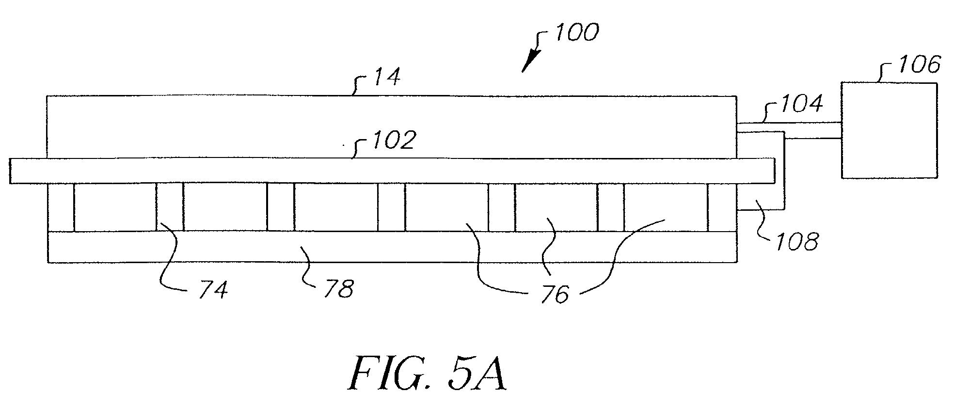
- FIG. 5a and b shows a display having an integrated touch screen and touch screen control components according to the present invention.
- An electroluminescent display generally designated 100 includes a single substrate 102 having a transistor switching matrix layer 74 and a light emission layer 78 containing materials of an electroluminescent display formed on one face of the substrate for emitting light through the substrate, touch sensitive elements 14 of a touch screen formed on the other face of the substrate 102, and a single flex-cable 104 that can be used for connecting the electroluminescent display 100 with external electronics 106 as disclosed in copending US Serial No. 09/855,449, filed concurrently by Feldman et al.
- the transistor switching matrix layer 74 contains thin film transistors 76 that in addition to providing control of the electroluminescent display, also implement a complete, or partial, resistive on-panel touch screen controller 112.
- the light emission layer 78 contains electroluminescent materials, located in the center part of the electroluminescent display, in an area called the active area 110 of the electroluminescent display.
- the substrate 102 is made of a transparent material, such as glass or plastic, and is thick enough to provide mechanical support for the transistor switching matrix layer 74, the light emission layer 78, and the touch sensitive elements 14.
- Conductors 108 connect the touch sensitive elements 14 to the touch screen controller 112, and are placed on the edges of the substrate 102.
- the cable 104 contains conductors that allow image data, display control signals, bias voltages, and touch screen signals to pass between external electronics 106 and the electroluminescent display 100.
- the number of conductors in the cable 104 of this embodiment is less than the number of conductors needed in the cable 16 (see Fig. 1a) plus in the cable 80 (see Fig. 3) in the prior art discussed above.
- This improved display eliminates the need for redundant conductors within the cable 104 and places some or all of the touch screen controller functionality within the display itself. This reduces the amount of raw materials in the system, therefore decreasing system cost, manufacturing cost, and system integration complexity.
- touch screen controller functionality may be implemented within the touch screen controller 112, based on system design constraints. Three embodiments are considered here.
- Fig. 6 shows an embodiment of the present invention where the touch screen controller circuit 112 includes an optional clock divider circuit 126, a voltage application circuit 34, and a multiplexing circuit 38.
- the touch detection circuit is implemented in external electronics 106 (see Fig. 5a). Voltages 120 and 122 applied to the touch screen controller circuit 112 are taken from voltages used for normal image display functions. When a touch occurs, the sensed change in voltage, and therefore resistance, is sent over cable 104 to an external controller for (X, Y) coordinate extraction.
- the clock divider circuit 126 divides an input clock pulse train 124 into a lower frequency.
- the input clock pulse train 124 is taken from a clock needed to control the image display, such as the pixel clock.
- the horizontal synchronization (HSYNC) or vertical synchronization (VSYNC) pulses may be used as the input clock, since these signals are periodic.
- these synchronization signals do not have a 50% duty cycle, as do most regular clock signals.
- a 50% duty cycle may be produced using these synchronization signals by using a frequency divider, such as the clock divider circuit 126.
- the pixel clock is usually the fastest of the three signals, followed by HSYNC, and then VSYNC.
- the pixel clock is approximately 30 MHz (assuming a transfer of one pixel per clock cycle)
- HSYNC is approximately 30 KHz
- VSYNC is 60 Hz.
- the signal closest in frequency to the needs of the touch screen controller may be selected, in order to minimize the size of the clock divider circuit 126.
- the output of the voltage application circuit 34 connects to the multiplexing circuit 38.
- the multiplexing circuit 38 includes circuitry that routes the appropriate voltages to the appropriate conductive elements within the touch sensitive elements 14 and the touch coordinate voltage to other circuitry for processing.
- the exact circuit implementation of the multiplexing circuit 38 is specific to the type of touch screen (4-wire or 5-wire). The specific embodiments of the multiplexing circuit 38 are discussed below.
- This embodiment of the touch screen controller circuit 112 has the advantages of placing a portion of the touch screen controller circuitry on the display itself, taking advantage of the thin film transistors lithography present in the manufacturing process of the image display.
- the touch screen controller circuit 112 is relatively simple and small in size, and also eliminates the need for two of the four conductors needed in the cable 104 for conventional 4-wire touch screen controllers by utilizing various signals needed for image display control and biasing.
- the touch screen controller circuit 112 eliminates the need for four of the five conductors needed in the cable 104 for conventional 5-wire touch screen controllers by utilizing various signals needed for image display control and biasing.
- the more transistor-intensive and area-intensive touch detection circuit 36 (see Fig. 1a) is placed in external electronics 106 (see Fig. 5a) on a printed circuit board, where conventional manufacturing processes for such circuitry are more efficient.
- Fig. 7 shows an embodiment of the present invention where the touch screen controller circuit 112 includes an optional clock divider circuit 126, a voltage application circuit 34, a multiplexing circuit 38, an analog-to-digital converter (ADC) 40, and a digital interface circuit 128.
- the operation of the clock divider circuit 126, the voltage application circuit 34, and the multiplexing circuit 38 are identical to that described in relation to the embodiment of Fig. 6.
- the touch voltage output of the multiplexing circuit 38 is routed to the input of analog-to-digital converter (ADC) 40 that converts the analog voltage measured by the touch sensitive elements into a digital form.
- ADC analog-to-digital converter
- the digitized voltage is transmitted, via digital interface circuit 128, over one or more conductors within cable 104 to a computation circuit 42 (see Fig. 2) in external electronics 106 (see Fig. 5a), where the digital voltage is converted to a touch coordinate.
- the digital interface circuit 128 may transmit the digital data serially or in parallel. Because human tactile response times are usually slow as compared to a display pixel clock, transmission of digital touch data is often performed serially, lowering the data rate, but eliminating one or more conductors associated with parallel transmission.
- the digital interface circuit 128 is usually synchronized to a known clock, such as the pixel clock. This embodiment has the advantage of converting the measured voltage to digital form before transmission over the cable 104 to external electronics on a printed circuit board. This significantly improves the noise immunity of the measured voltage, allowing for a more accurate touch position calculation.
- Fig. 8 shows an embodiment of the present invention where the touch screen controller circuit 112 includes an optional clock divider circuit 126, a voltage application circuit 34, a multiplexing circuit 38, an analog-to-digital converter (ADC) 40, a computation circuit 42, and a digital interface circuit 128.
- the operation of the clock divider circuit 126, the voltage application circuit 34, the multiplexing circuit 38, the analog-to-digital converter 40, and the digital interface circuit 128 are identical to that described in relation to the embodiment of Fig. 7.
- the output of the analog-to-digital converter 40 is routed to the input of the computation circuit 42.
- the computation circuit 42 allows the touch screen coordinate to be computed on the electroluminescent display itself, and the touch screen coordinate to be transmitted to external electronics 106 (see Fig. 5a) via the digital interface circuit 128.
- This embodiment has the advantage of producing the touch screen coordinate on the electroluminescent display 100 itself.
- the entire touch screen function is then contained in one device, improving system design via improved partitioning of circuit functions. Additional circuitry is not required in the external electronics 106 (see Fig. 5a) for resistive touch screen operation, improving time-to-market for systems containing an electroluminescent display 100.
- Fig. 9 shows the electrical structure of a prior art 4-wire resistive touch screen.
- the lower circuit layer 20 contains two parallel metal bars 50 and 51 oriented in one direction, and a resistive ITO coating 54 extending between the metal bars 50 and 51.
- the upper circuit layer 26 contains two metal bars 52 and 53 perpendicular to metal bars 50 and 51, and a resistive ITO coating 56 extending between the metal bars 52 and 53.
- the lower circuit layer 20 and the upper circuit layer 26 are separated by a flexible spacer layer 22 (see Fig. 1b) containing a matrix of spacer dots.
- an external touch screen controller applies a voltage between two parallel metal bars, forming a voltage gradient in the intervening resistive ITO coating. The other two parallel metal bars are then used as voltage probe points.
- the touch detection circuit 36 monitors the voltage read from the touch screen, decides when a touch has been performed, and computes the (X, Y) coordinates of the touch point the voltage placed across the first two parallel metal bars. To measure the X coordinate, a voltage gradient is applied to parallel metal bars 52 and 53. To measure the Y coordinate, a voltage gradient is applied to parallel metal bars 50 and 51.
- An improved flat panel display and 4-wire resistive touch screen system utilizes a single substrate incorporating touch sensitive elements, light emitting materials, a single cable, and touch screen controller circuitry.
- Fig. 10a and b show this embodiment.
- the touch sensitive elements 14 shown in Fig. 5a implement a 4-wire resistive touch screen in the embodiment of Figs. 10a and 10b, and are placed on the top of the substrate 102.
- An electroluminescent display having an active area 110 is formed on the bottom of the substrate 102.
- Circuitry 112 implementing a portion or all of a resistive touch screen controller is also formed on the bottom face of the substrate 102.
- Metal bars 50, 51, 52 and 53 in the resistive touch screen elements are connected to the resistive touch screen controller 112 via conductors 108.
- touch screen controller functionality may be implemented within the touch screen controller 112, based on system design constraints, as described in relation to Figs. 6, 7 and 8.
- This circuitry may be used for both 5-wire and 4-wire touch screens.
- the main difference between implementations for the two types of touch screens is the implementation of the multiplexing circuit 38.
- Fig. 11 shows an embodiment of the present invention for a voltage application circuit 34 and a multiplexing circuit 38 used with a 4-wire touch screen.
- the voltage application circuit 34 contains circuitry that selects how the voltages are applied to the electrodes of the touch sensitive elements 14, and therefore controls the coordinate of the point of touch being read.
- the voltage application circuit 34 consists of an X/Y coordinate selection circuit 129 and an inverter 130.
- the X/Y coordinate selection circuit 129 is typically a flip-flop that may be toggled on each cycle of its input clock. When the flip-flop is in the low state, the X coordinate is being measured. When the flip-flop is in the high state, the Y coordinate is being measured.
- An inverter 130 is used to produce the inverse of the flip-flop output.
- the multiplexing circuit 38 contains four analog tristate buffers 134, 136, 138 and 140, and two electronic switches 142 and 144.
- Each tristate buffer drives its input voltage to the appropriate metal bars when enabled, and prevents voltage transmission when disabled.
- a logic high on a tristate buffer's enable input allows the input voltage to pass to the output, while a logic low disables the transmission of the input voltage to the output.
- Each electronic switch passes one of two input voltages to its output, based on the logic level of its voltage selection signal.
- a logic high on the voltage selection signal passes the upper input voltage to the output of the electronic switch, as drawn in Fig. 11.
- a logic low on the voltage selection signal passes the lower input voltage to the output of the electronic switch.
- tristate buffers 136 and 140 are enabled, while tristate buffers 134 and 138 are disabled.
- voltage 120 is placed on metal bar 52 and voltage 122 is placed on metal bar 53.
- Metal bars 50 and 51 are not driven by either voltage 120 or 122.
- a voltage gradient is then placed across resistive ITO coating 56, allowing a touch to be detected in the X direction.
- a touch occurs, a voltage proportional to the X coordinate of the touch location is transferred to the resistive ITO coating 54 in the lower circuit layer 20. Accordingly, voltages are transferred to metal bars 50 and 51.
- Electronic switches 142 and 144 then transfer these voltages to an analog-to-digital converter (not shown) or conductors within a cable (not shown). Using these voltages, the X coordinate of the touch location may be computed.
- Fig. 12 shows the electrical structure of a prior art 5-wire resistive touch screen.
- the lower circuit layer 20 contains four metal electrodes 60, 61, 62 and 63 located at the corners, connected to a resistive ITO coating 64.
- the four metal electrodes 60, 61, 62 and 63 also connect to four conductors in cable 16.
- Also in the lower circuit layer is a metal electrode 66 that connects to a conductor in cable 16.
- the upper circuit layer 26 contains one metal electrode 65 connected to a transparent metal conductive area 68.
- a flexible spacer layer (not shown) separates the lower circuit layer 20 and the upper circuit layer 26. When manufactured, metal contacts 65 and 66 are electrically connected together, transferring the voltage on the transparent metal conductive area 68 to the cable 16.
- an external touch screen controller applies voltages to the four metal electrodes 60, 61, 62 and 63, forming a voltage gradient in the intervening resistive ITO coating 64.
- two of these four metal electrodes always have a constant voltage applied to them.
- the two metal electrodes held to constant voltages are usually diagonal to each other; for example, metal electrode 60 would have a constant voltage 5V, and metal electrode 63 would have a constant voltage 0V.
- the coordinate measured then depends on the voltage applied to the remaining two metal electrodes 61 and 62.
- the fifth metal electrode 65 is used as a voltage probe point. When the touch occurs, resistive ITO coatings 64 and the transparent metal conductive area 68 are shorted at the point of contact.
- the voltage at that point on the resistive ITO coating is transferred to the transparent metal conductive area, the attached metal electrode 65, and to the touch detection circuit 36 (see Fig. 1a) within external touch screen controller 18 (see Fig. 1a) via a conductor in cable 16.
- the touch detection circuit monitors the voltage read from the touch screen, decides when a touch has been performed, and computes the (X, Y) coordinates of the touch point.
- a voltage gradient is placed across the resistive ITO coating 64 in the X-direction. To do so, 5V would be applied to metal electrode 62 and 0V would be applied to metal electrode 61. To measure the Y coordinate, 5V would be applied to metal electrode 61 and 0V would be applied to metal electrode 62.
- 5-wire touch screen controller functionality may be implemented within the touch screen controller 112 located on the electroluminescent display side of the substrate, based on system design constraints, as described in relation to Figs. 6, 7 and 8.
- the multiplexing circuit 38 is significantly different for a 5-wire touch screen controller.
- Fig. 14 shows an embodiment of the present invention for a voltage application circuit 34 and a multiplexing circuit 38 used with a 5-wire touch screen.
- the voltage application circuit 34 contains an X/Y coordinate selection circuit 129. No inverter is needed, as is required for the 4-wire embodiment. Otherwise, the operation of the voltage application circuit 34 is equivalent to that of the 4-wire embodiment described in relation to Fig. 11.
- the multiplexing circuit 38 consists of two electronic switches 148 and 150 that determine the voltage sent to metal electrodes 61 and 62.
- Metal electrode 60 is set to voltage 120 while metal electrode 63 is set to voltage 122.
Landscapes
- Engineering & Computer Science (AREA)
- General Engineering & Computer Science (AREA)
- Theoretical Computer Science (AREA)
- Human Computer Interaction (AREA)
- Physics & Mathematics (AREA)
- General Physics & Mathematics (AREA)
- Position Input By Displaying (AREA)
- Electroluminescent Light Sources (AREA)
- Control Of Indicators Other Than Cathode Ray Tubes (AREA)
- Devices For Indicating Variable Information By Combining Individual Elements (AREA)
Abstract
Description
Claims (18)
- An organic electroluminescent display with integrated touch screen, comprising:a) a transparent substrate having two faces;b) a transistor switching matrix and a light emitting layer forming an active matrix electroluminescent display located on one face of the substrate for emitting light through the substrate;c) touch sensitive elements of a touch screen located on the other face of the substrate;d) components of a touch screen controller located on the one face of the substrate; ande) an electrical connector for connecting the components of the touch screen controller on the one face of the substrate to the touch screen elements on the other face of the substrate.
- The display of claim 1, wherein the electroluminescent display is an organic light emitting diode display (OLED).
- The display of claim 1, wherein the touch screen is a resistive touch screen, and the touch screen controller is a resistive touch screen controller.
- The display of claim 3, where the resistive touch screen is 4-wire.
- The display of claim 3, where the resistive touch screen is 5-wire.
- The display of claim 3, wherein the touch screen controller is responsive to control signals that control the electroluminescent display.
- The display of claim 1, wherein the electrical connector contains fewer conductors than is required if the touch screen controller is located external to the organic electroluminescent display.
- The display of claim 1, wherein the substrate is glass.
- The display of claim 1, wherein the substrate is plastic.
- The display of claim 1, wherein the components of the touch screen located on the one face of the substrate comprise:a) a voltage application circuit responsive to signals present for control of the light emitting elements, andb) a multiplexing circuit for selection of voltage application to the touch sensitive elements and for routing the measured voltage gradient in analog form to the electrical connector for computation by an external controller.
- The display of claim 10, wherein the components of the touch screen located on the one face of the substrate, further comprise an analog-to-digital converter for converting a measured analog voltage to digital format for transmission over to the electrical connector for computation by an external controller.
- The display of claim 11, wherein the components of the touch screen located on the one face of the substrate, further comprise a computation circuit for computing the coordinate of a touch.
- The display of claim 1, further comprising means for generating a periodic signal for synchronizing the electroluminescent display operations and the touch screen controller.
- The display of claim 13, wherein the periodic signal is a clock signal.
- The display of claim 14, where the clock signal is a pixel clock.
- The display of claim 13, further comprising a divider circuit located in the touch screen controller to produce a lower periodic frequency signal for synchronizing the touch screen controller.
- The display of claim 13, where the periodic signal is a horizontal synchronization signal.
- The display of claim 13, where the periodic signal is a vertical synchronization signal.
Applications Claiming Priority (2)
| Application Number | Priority Date | Filing Date | Title |
|---|---|---|---|
| US855452 | 2001-05-15 | ||
| US09/855,452 US6424094B1 (en) | 2001-05-15 | 2001-05-15 | Organic electroluminescent display with integrated resistive touch screen |
Publications (2)
| Publication Number | Publication Date |
|---|---|
| EP1258922A2 true EP1258922A2 (en) | 2002-11-20 |
| EP1258922A3 EP1258922A3 (en) | 2006-07-05 |
Family
ID=25321296
Family Applications (1)
| Application Number | Title | Priority Date | Filing Date |
|---|---|---|---|
| EP02076758A Withdrawn EP1258922A3 (en) | 2001-05-15 | 2002-05-03 | Organic electroluminescent display with integrated resistive touch screen |
Country Status (6)
| Country | Link |
|---|---|
| US (1) | US6424094B1 (en) |
| EP (1) | EP1258922A3 (en) |
| JP (1) | JP2002359078A (en) |
| KR (1) | KR20020087359A (en) |
| CN (1) | CN1385814A (en) |
| TW (1) | TW546675B (en) |
Cited By (3)
| Publication number | Priority date | Publication date | Assignee | Title |
|---|---|---|---|---|
| EP1351124A3 (en) * | 2002-04-03 | 2005-11-16 | Pioneer Corporation | Display portion integrated type touch panel apparatus and method for manufacturing the same |
| DE10361185B4 (en) * | 2002-12-24 | 2015-04-09 | Lg Display Co., Ltd. | A touch-sensitive single-unit liquid crystal display panel and method of manufacturing the same |
| EP2869346B1 (en) * | 2009-06-08 | 2022-05-25 | LG Display Co., Ltd. | Organic light emitting diode display |
Families Citing this family (87)
| Publication number | Priority date | Publication date | Assignee | Title |
|---|---|---|---|---|
| US6674562B1 (en) | 1994-05-05 | 2004-01-06 | Iridigm Display Corporation | Interferometric modulation of radiation |
| US7138984B1 (en) * | 2001-06-05 | 2006-11-21 | Idc, Llc | Directly laminated touch sensitive screen |
| US6680792B2 (en) | 1994-05-05 | 2004-01-20 | Iridigm Display Corporation | Interferometric modulation of radiation |
| US6073497A (en) * | 1997-08-05 | 2000-06-13 | Micron Technology, Inc. | High resolution pressure sensing device having an insulating flexible matrix loaded with filler particles |
| WO1999052006A2 (en) | 1998-04-08 | 1999-10-14 | Etalon, Inc. | Interferometric modulation of radiation |
| US6424339B1 (en) * | 2000-06-16 | 2002-07-23 | The Bergquist Company | Touch screen assembly |
| US6611257B1 (en) * | 2000-09-29 | 2003-08-26 | Rockwell Automation Technologies, Inc. | Automatic detection of touch plane type |
| US6814642B2 (en) * | 2001-04-04 | 2004-11-09 | Eastman Kodak Company | Touch screen display and method of manufacture |
| CA2353697A1 (en) * | 2001-07-24 | 2003-01-24 | Tactex Controls Inc. | Touch sensitive membrane |
| GB0119070D0 (en) * | 2001-08-06 | 2001-09-26 | Ibm | Method and apparatus for managing a loop network |
| US7158121B2 (en) * | 2001-10-19 | 2007-01-02 | American Standard International Inc. | Enhanced touch-screen display system |
| US20030117378A1 (en) | 2001-12-21 | 2003-06-26 | International Business Machines Corporation | Device and system for retrieving and displaying handwritten annotations |
| US20030150107A1 (en) * | 2002-02-08 | 2003-08-14 | Eastman Kodak Company | Method for manufacturing an integrated display device including an OLED display and a touch screen |
| KR20030069707A (en) * | 2002-02-22 | 2003-08-27 | 엘지.필립스 엘시디 주식회사 | Organic Electroluminescent Device and Method for Fabricating the same |
| US9153168B2 (en) * | 2002-07-09 | 2015-10-06 | Semiconductor Energy Laboratory Co., Ltd. | Method for deciding duty factor in driving light-emitting device and driving method using the duty factor |
| US7781850B2 (en) | 2002-09-20 | 2010-08-24 | Qualcomm Mems Technologies, Inc. | Controlling electromechanical behavior of structures within a microelectromechanical systems device |
| US7936338B2 (en) | 2002-10-01 | 2011-05-03 | Sony Corporation | Display unit and its manufacturing method |
| US6879319B2 (en) * | 2002-10-25 | 2005-04-12 | Eastman Kodak Company | Integrated OLED display and touch screen |
| US7362313B2 (en) * | 2003-01-17 | 2008-04-22 | 3M Innovative Properties Company | Touch simulation system and method |
| FR2851346B1 (en) * | 2003-02-13 | 2005-07-01 | Gabriel Pascal Joseph Simon | INTERACTIVE SCREEN FOR ACQUIRING AND RETRIEVING GRAPHIC INFORMATION MANUALLY ENTERED |
| US7310779B2 (en) | 2003-06-26 | 2007-12-18 | International Business Machines Corporation | Method for creating and selecting active regions on physical documents |
| KR101023500B1 (en) | 2003-08-18 | 2011-03-21 | 군제 가부시키가이샤 | Transparent touch panel and electronic device |
| US6885157B1 (en) | 2003-11-25 | 2005-04-26 | Eastman Kodak Company | Integrated touch screen and OLED flat-panel display |
| US20050174335A1 (en) * | 2004-02-10 | 2005-08-11 | Elo Touchsystems, Inc. | Resistive touchscreen with programmable display coversheet |
| KR101313117B1 (en) | 2004-07-29 | 2013-09-30 | 퀄컴 엠이엠에스 테크놀로지스, 인크. | System and method for micro-electromechanical operating of an interferometric modulator |
| US7535466B2 (en) | 2004-09-27 | 2009-05-19 | Idc, Llc | System with server based control of client device display features |
| US7653371B2 (en) | 2004-09-27 | 2010-01-26 | Qualcomm Mems Technologies, Inc. | Selectable capacitance circuit |
| US7586484B2 (en) | 2004-09-27 | 2009-09-08 | Idc, Llc | Controller and driver features for bi-stable display |
| US7373026B2 (en) * | 2004-09-27 | 2008-05-13 | Idc, Llc | MEMS device fabricated on a pre-patterned substrate |
| US7460246B2 (en) | 2004-09-27 | 2008-12-02 | Idc, Llc | Method and system for sensing light using interferometric elements |
| US7317568B2 (en) | 2004-09-27 | 2008-01-08 | Idc, Llc | System and method of implementation of interferometric modulators for display mirrors |
| US7369296B2 (en) | 2004-09-27 | 2008-05-06 | Idc, Llc | Device and method for modifying actuation voltage thresholds of a deformable membrane in an interferometric modulator |
| US7369294B2 (en) | 2004-09-27 | 2008-05-06 | Idc, Llc | Ornamental display device |
| US7920135B2 (en) | 2004-09-27 | 2011-04-05 | Qualcomm Mems Technologies, Inc. | Method and system for driving a bi-stable display |
| US7583429B2 (en) | 2004-09-27 | 2009-09-01 | Idc, Llc | Ornamental display device |
| US7808703B2 (en) | 2004-09-27 | 2010-10-05 | Qualcomm Mems Technologies, Inc. | System and method for implementation of interferometric modulator displays |
| US7327510B2 (en) * | 2004-09-27 | 2008-02-05 | Idc, Llc | Process for modifying offset voltage characteristics of an interferometric modulator |
| JP4622432B2 (en) * | 2004-09-30 | 2011-02-02 | セイコーエプソン株式会社 | Touch panel control unit |
| CN100379056C (en) * | 2005-03-01 | 2008-04-02 | 友达光电股份有限公司 | Flat panel display with touch control function and forming method thereof |
| TWI270025B (en) * | 2005-03-21 | 2007-01-01 | Au Optronics Corp | Dual emission display with integrated touch screen and fabricating method thereof |
| EP2495212A3 (en) * | 2005-07-22 | 2012-10-31 | QUALCOMM MEMS Technologies, Inc. | Mems devices having support structures and methods of fabricating the same |
| US20100020045A1 (en) * | 2005-08-18 | 2010-01-28 | Kevin Walsh | Optically enhanced flat panel display system having integral touch screen |
| EP1928780A2 (en) | 2005-09-30 | 2008-06-11 | Qualcomm Mems Technologies, Inc. | Mems device and interconnects for same |
| US7916980B2 (en) | 2006-01-13 | 2011-03-29 | Qualcomm Mems Technologies, Inc. | Interconnect structure for MEMS device |
| US7652814B2 (en) | 2006-01-27 | 2010-01-26 | Qualcomm Mems Technologies, Inc. | MEMS device with integrated optical element |
| US7582952B2 (en) | 2006-02-21 | 2009-09-01 | Qualcomm Mems Technologies, Inc. | Method for providing and removing discharging interconnect for chip-on-glass output leads and structures thereof |
| US8144115B2 (en) | 2006-03-17 | 2012-03-27 | Konicek Jeffrey C | Flat panel display screen operable for touch position determination system and methods |
| US7643203B2 (en) * | 2006-04-10 | 2010-01-05 | Qualcomm Mems Technologies, Inc. | Interferometric optical display system with broadband characteristics |
| US7903047B2 (en) | 2006-04-17 | 2011-03-08 | Qualcomm Mems Technologies, Inc. | Mode indicator for interferometric modulator displays |
| US7417784B2 (en) | 2006-04-19 | 2008-08-26 | Qualcomm Mems Technologies, Inc. | Microelectromechanical device and method utilizing a porous surface |
| US7859526B2 (en) * | 2006-05-01 | 2010-12-28 | Konicek Jeffrey C | Active matrix emissive display and optical scanner system, methods and applications |
| US7369292B2 (en) * | 2006-05-03 | 2008-05-06 | Qualcomm Mems Technologies, Inc. | Electrode and interconnect materials for MEMS devices |
| US20070268201A1 (en) * | 2006-05-22 | 2007-11-22 | Sampsell Jeffrey B | Back-to-back displays |
| US7566664B2 (en) | 2006-08-02 | 2009-07-28 | Qualcomm Mems Technologies, Inc. | Selective etching of MEMS using gaseous halides and reactive co-etchants |
| US7812827B2 (en) | 2007-01-03 | 2010-10-12 | Apple Inc. | Simultaneous sensing arrangement |
| US20080231605A1 (en) * | 2007-03-21 | 2008-09-25 | Kai-Ti Yang | Compound touch panel |
| US7733552B2 (en) | 2007-03-21 | 2010-06-08 | Qualcomm Mems Technologies, Inc | MEMS cavity-coating layers and methods |
| US7719752B2 (en) | 2007-05-11 | 2010-05-18 | Qualcomm Mems Technologies, Inc. | MEMS structures, methods of fabricating MEMS components on separate substrates and assembly of same |
| US8493331B2 (en) | 2007-06-13 | 2013-07-23 | Apple Inc. | Touch detection using multiple simultaneous frequencies |
| US20090009483A1 (en) * | 2007-06-13 | 2009-01-08 | Apple Inc. | Single-chip touch controller with integrated drive system |
| US7876311B2 (en) * | 2007-06-13 | 2011-01-25 | Apple Inc. | Detection of low noise frequencies for multiple frequency sensor panel stimulation |
| US7570415B2 (en) | 2007-08-07 | 2009-08-04 | Qualcomm Mems Technologies, Inc. | MEMS device and interconnects for same |
| KR100916321B1 (en) | 2007-12-17 | 2009-09-11 | 한국전자통신연구원 | Organic light emitting diode touch screen device and manufacturing method thereof |
| KR100902211B1 (en) * | 2008-03-13 | 2009-06-11 | 삼성모바일디스플레이주식회사 | Touch panel integrated organic light emitting display device |
| JP5178817B2 (en) * | 2008-03-31 | 2013-04-10 | シャープ株式会社 | Display device, electronic device including the same, and touch panel |
| CN101576795B (en) * | 2008-05-06 | 2011-05-18 | 比亚迪股份有限公司 | Touch screen body and resistance type touch screen using same |
| KR20100024710A (en) * | 2008-08-26 | 2010-03-08 | 삼성모바일디스플레이주식회사 | Organic light emitting diode display |
| KR101097453B1 (en) * | 2008-09-09 | 2011-12-23 | 네오뷰코오롱 주식회사 | Keypad apparatus, mobile device having the same and keypad control method |
| KR101045264B1 (en) * | 2008-09-09 | 2011-06-29 | 네오뷰코오롱 주식회사 | Display device, mobile device having same and display control method |
| US9606663B2 (en) | 2008-09-10 | 2017-03-28 | Apple Inc. | Multiple stimulation phase determination |
| US8592697B2 (en) | 2008-09-10 | 2013-11-26 | Apple Inc. | Single-chip multi-stimulus sensor controller |
| US9348451B2 (en) | 2008-09-10 | 2016-05-24 | Apple Inc. | Channel scan architecture for multiple stimulus multi-touch sensor panels |
| US20100137033A1 (en) * | 2008-11-28 | 2010-06-03 | Elan Microelectronics Corp. | Illuminated Touch Sensitive Surface Module |
| TWI409677B (en) * | 2008-11-28 | 2013-09-21 | Elan Microelectronics Corp | Illuminated touchpad module and illuminated device thereof |
| TWI442292B (en) * | 2009-04-21 | 2014-06-21 | Ind Tech Res Inst | Touch display apparatus and fabricating method thereof |
| TWI463452B (en) * | 2009-04-21 | 2014-12-01 | Ind Tech Res Inst | Touch display apparatus and fabricating method thereof |
| KR101577827B1 (en) * | 2009-06-24 | 2015-12-16 | 엘지디스플레이 주식회사 | Organic electroluminescent display device |
| US9036650B2 (en) * | 2009-09-11 | 2015-05-19 | Apple Inc. | Automatic low noise frequency selection |
| KR20110037337A (en) * | 2009-10-06 | 2011-04-13 | 엘지디스플레이 주식회사 | Organic light emitting display device and manufacturing method thereof |
| IT1400746B1 (en) | 2010-06-30 | 2013-07-02 | Damian S R L | AUTOMATIC PRODUCT DISTRIBUTOR MACHINE |
| KR101329461B1 (en) * | 2010-11-25 | 2013-11-15 | 엘지디스플레이 주식회사 | Display device having touch screen panel |
| WO2013056438A1 (en) * | 2011-10-19 | 2013-04-25 | Tpk Touch Solutions Inc. | Touch sensitive display |
| US9215779B2 (en) * | 2012-03-30 | 2015-12-15 | Cooper Technologies Company | Light switch and control device having a touch screen interface |
| US10254815B2 (en) * | 2013-03-08 | 2019-04-09 | Microchip Technology Incorporated | Using capacitive proximity detection with resistive touch screens for wake-up |
| CN106775040B (en) * | 2015-11-20 | 2019-09-24 | 京东方科技集团股份有限公司 | Control device, touch screen and the display device of electroluminescent touch-control display panel |
| CN110969982B (en) * | 2018-09-28 | 2022-09-13 | 北京小米移动软件有限公司 | Display structure, display panel and display device |
| KR102945456B1 (en) * | 2021-04-12 | 2026-04-01 | 삼성디스플레이 주식회사 | Display device |
Family Cites Families (6)
| Publication number | Priority date | Publication date | Assignee | Title |
|---|---|---|---|---|
| US4893115A (en) * | 1985-11-12 | 1990-01-09 | John Fluke Mfg. Co., Inc. | Touch sensitive visual display system |
| JPH08265558A (en) | 1994-12-26 | 1996-10-11 | Ricoh Co Ltd | Image forming device |
| US6035180A (en) * | 1997-10-07 | 2000-03-07 | Ericsson Inc. | Communication module having selectively programmable exterior surface |
| JP2000331557A (en) * | 1999-05-21 | 2000-11-30 | Mimaki Denshi Buhin Kk | Light-emitting display device with touch panel sensor |
| JP2001051608A (en) * | 1999-08-06 | 2001-02-23 | Minolta Co Ltd | Display device |
| JP2001076886A (en) * | 1999-09-03 | 2001-03-23 | Futaba Corp | Organic EL device with transparent touch switch and method of manufacturing the same |
-
2001
- 2001-05-15 US US09/855,452 patent/US6424094B1/en not_active Expired - Lifetime
-
2002
- 2002-03-26 TW TW091105920A patent/TW546675B/en not_active IP Right Cessation
- 2002-05-03 EP EP02076758A patent/EP1258922A3/en not_active Withdrawn
- 2002-05-14 JP JP2002138701A patent/JP2002359078A/en active Pending
- 2002-05-14 KR KR1020020026349A patent/KR20020087359A/en not_active Withdrawn
- 2002-05-15 CN CN02119361A patent/CN1385814A/en active Pending
Cited By (4)
| Publication number | Priority date | Publication date | Assignee | Title |
|---|---|---|---|---|
| EP1351124A3 (en) * | 2002-04-03 | 2005-11-16 | Pioneer Corporation | Display portion integrated type touch panel apparatus and method for manufacturing the same |
| KR100654680B1 (en) | 2002-04-03 | 2006-12-07 | 파이오니아 가부시키가이샤 | Display unit integrated touch panel device and manufacturing method thereof |
| DE10361185B4 (en) * | 2002-12-24 | 2015-04-09 | Lg Display Co., Ltd. | A touch-sensitive single-unit liquid crystal display panel and method of manufacturing the same |
| EP2869346B1 (en) * | 2009-06-08 | 2022-05-25 | LG Display Co., Ltd. | Organic light emitting diode display |
Also Published As
| Publication number | Publication date |
|---|---|
| TW546675B (en) | 2003-08-11 |
| US6424094B1 (en) | 2002-07-23 |
| CN1385814A (en) | 2002-12-18 |
| JP2002359078A (en) | 2002-12-13 |
| EP1258922A3 (en) | 2006-07-05 |
| KR20020087359A (en) | 2002-11-22 |
Similar Documents
| Publication | Publication Date | Title |
|---|---|---|
| US6424094B1 (en) | Organic electroluminescent display with integrated resistive touch screen | |
| KR102570350B1 (en) | Touch display device, touch system, driving circuit, and driving method | |
| JP5925279B2 (en) | Display device and driving method thereof | |
| US10185170B2 (en) | Display device | |
| CN107783689B (en) | Driver chip, circuit film, chip-on-film type driver circuit, and display device | |
| TW201931092A (en) | Touch display device, touch system, touch driving circuit, pen, and pen sensing method | |
| KR20190081532A (en) | Touch display device, touch driving circuit, and touch driving method | |
| KR101350876B1 (en) | Display device and control method of the same | |
| TWI546720B (en) | Touch screen and related touch sensing control circuit | |
| CN107801415A (en) | Combining ability and touch sensor | |
| KR20200073342A (en) | Testing device of display module, testing system having the same and testing method of the same | |
| CN107678597B (en) | A touch display panel and a touch display device | |
| US20210096721A1 (en) | Techniques for routing signals using inactive sensor regions of touch sensors and related systems and devices | |
| US9361847B2 (en) | Display device and driving method thereof | |
| KR20150043801A (en) | Touch panel display device | |
| KR102945456B1 (en) | Display device | |
| KR20180025774A (en) | Driving chip, circuit film, chip on film typed driving circuit, and display device with a built-in touch screen | |
| KR20240068460A (en) | Touch display device and touch sensing method | |
| KR102958081B1 (en) | Display device | |
| KR102954241B1 (en) | Touch display device, driving circuit and method for driving it | |
| US20180157084A1 (en) | Detection device | |
| US12101983B2 (en) | Display device equipped with touch panel, and method for controlling display device | |
| KR102469011B1 (en) | Display device integrated with touch screen panel and method for driving the display device integrated with touch screen panel | |
| KR20240065976A (en) | Touch display device and touch sensing method | |
| KR20180069280A (en) | Multi point touch screen pannel |
Legal Events
| Date | Code | Title | Description |
|---|---|---|---|
| PUAI | Public reference made under article 153(3) epc to a published international application that has entered the european phase |
Free format text: ORIGINAL CODE: 0009012 |
|
| AK | Designated contracting states |
Kind code of ref document: A2 Designated state(s): AT BE CH CY DE DK ES FI FR GB GR IE IT LI LU MC NL PT SE TR |
|
| AX | Request for extension of the european patent |
Free format text: AL;LT;LV;MK;RO;SI |
|
| PUAL | Search report despatched |
Free format text: ORIGINAL CODE: 0009013 |
|
| RIC1 | Information provided on ipc code assigned before grant |
Ipc: H01L 27/15 20060101AFI20060504BHEP |
|
| AK | Designated contracting states |
Kind code of ref document: A3 Designated state(s): AT BE CH CY DE DK ES FI FR GB GR IE IT LI LU MC NL PT SE TR |
|
| AX | Request for extension of the european patent |
Extension state: AL LT LV MK RO SI |
|
| AKX | Designation fees paid | ||
| REG | Reference to a national code |
Ref country code: DE Ref legal event code: 8566 |
|
| STAA | Information on the status of an ep patent application or granted ep patent |
Free format text: STATUS: THE APPLICATION IS DEEMED TO BE WITHDRAWN |
|
| 18D | Application deemed to be withdrawn |
Effective date: 20061201 |