EP1258770A1 - Optical switch - Google Patents
Optical switch Download PDFInfo
- Publication number
- EP1258770A1 EP1258770A1 EP01272272A EP01272272A EP1258770A1 EP 1258770 A1 EP1258770 A1 EP 1258770A1 EP 01272272 A EP01272272 A EP 01272272A EP 01272272 A EP01272272 A EP 01272272A EP 1258770 A1 EP1258770 A1 EP 1258770A1
- Authority
- EP
- European Patent Office
- Prior art keywords
- light
- optical
- light transmission
- optical path
- optical switch
- Prior art date
- Legal status (The legal status is an assumption and is not a legal conclusion. Google has not performed a legal analysis and makes no representation as to the accuracy of the status listed.)
- Granted
Links
- 230000003287 optical effect Effects 0.000 title claims abstract description 628
- 230000005540 biological transmission Effects 0.000 claims abstract description 327
- 238000006073 displacement reaction Methods 0.000 claims abstract description 76
- 230000004044 response Effects 0.000 claims abstract description 10
- 230000007246 mechanism Effects 0.000 claims abstract description 5
- 239000000919 ceramic Substances 0.000 claims description 47
- 239000000758 substrate Substances 0.000 claims description 43
- 238000000149 argon plasma sintering Methods 0.000 claims description 25
- 239000013307 optical fiber Substances 0.000 claims description 13
- 238000005452 bending Methods 0.000 claims description 9
- 238000010304 firing Methods 0.000 claims description 9
- 239000012780 transparent material Substances 0.000 claims description 9
- 238000005304 joining Methods 0.000 claims description 7
- 238000005245 sintering Methods 0.000 claims description 6
- 230000010354 integration Effects 0.000 abstract description 7
- 230000009467 reduction Effects 0.000 abstract description 4
- 238000005549 size reduction Methods 0.000 abstract description 4
- 239000010410 layer Substances 0.000 description 101
- 239000000463 material Substances 0.000 description 64
- 238000000034 method Methods 0.000 description 55
- 239000010408 film Substances 0.000 description 22
- 239000013078 crystal Substances 0.000 description 17
- 238000003475 lamination Methods 0.000 description 16
- 239000000203 mixture Substances 0.000 description 16
- 229910052751 metal Inorganic materials 0.000 description 14
- 239000002184 metal Substances 0.000 description 14
- 239000002243 precursor Substances 0.000 description 14
- RVTZCBVAJQQJTK-UHFFFAOYSA-N oxygen(2-);zirconium(4+) Chemical compound [O-2].[O-2].[Zr+4] RVTZCBVAJQQJTK-UHFFFAOYSA-N 0.000 description 13
- 229910001928 zirconium oxide Inorganic materials 0.000 description 13
- 238000004891 communication Methods 0.000 description 12
- 239000011521 glass Substances 0.000 description 12
- 239000011347 resin Substances 0.000 description 12
- 229920005989 resin Polymers 0.000 description 12
- BASFCYQUMIYNBI-UHFFFAOYSA-N platinum Chemical compound [Pt] BASFCYQUMIYNBI-UHFFFAOYSA-N 0.000 description 11
- 239000007788 liquid Substances 0.000 description 10
- 230000008901 benefit Effects 0.000 description 9
- 238000004519 manufacturing process Methods 0.000 description 9
- 239000000843 powder Substances 0.000 description 9
- XEEYBQQBJWHFJM-UHFFFAOYSA-N Iron Chemical compound [Fe] XEEYBQQBJWHFJM-UHFFFAOYSA-N 0.000 description 8
- 239000012071 phase Substances 0.000 description 8
- 230000002829 reductive effect Effects 0.000 description 8
- 238000007650 screen-printing Methods 0.000 description 8
- KDLHZDBZIXYQEI-UHFFFAOYSA-N Palladium Chemical compound [Pd] KDLHZDBZIXYQEI-UHFFFAOYSA-N 0.000 description 7
- 238000010438 heat treatment Methods 0.000 description 7
- PXHVJJICTQNCMI-UHFFFAOYSA-N Nickel Chemical compound [Ni] PXHVJJICTQNCMI-UHFFFAOYSA-N 0.000 description 6
- 230000006870 function Effects 0.000 description 6
- 239000012535 impurity Substances 0.000 description 6
- 238000003754 machining Methods 0.000 description 6
- VYPSYNLAJGMNEJ-UHFFFAOYSA-N silicon dioxide Inorganic materials O=[Si]=O VYPSYNLAJGMNEJ-UHFFFAOYSA-N 0.000 description 6
- GWEVSGVZZGPLCZ-UHFFFAOYSA-N Titan oxide Chemical compound O=[Ti]=O GWEVSGVZZGPLCZ-UHFFFAOYSA-N 0.000 description 5
- 239000000853 adhesive Substances 0.000 description 5
- 230000001070 adhesive effect Effects 0.000 description 5
- 239000002313 adhesive film Substances 0.000 description 5
- 238000005229 chemical vapour deposition Methods 0.000 description 5
- RKTYLMNFRDHKIL-UHFFFAOYSA-N copper;5,10,15,20-tetraphenylporphyrin-22,24-diide Chemical compound [Cu+2].C1=CC(C(=C2C=CC([N-]2)=C(C=2C=CC=CC=2)C=2C=CC(N=2)=C(C=2C=CC=CC=2)C2=CC=C3[N-]2)C=2C=CC=CC=2)=NC1=C3C1=CC=CC=C1 RKTYLMNFRDHKIL-UHFFFAOYSA-N 0.000 description 5
- 230000005684 electric field Effects 0.000 description 5
- 238000000465 moulding Methods 0.000 description 5
- TWNQGVIAIRXVLR-UHFFFAOYSA-N oxo(oxoalumanyloxy)alumane Chemical compound O=[Al]O[Al]=O TWNQGVIAIRXVLR-UHFFFAOYSA-N 0.000 description 5
- 239000002002 slurry Substances 0.000 description 5
- 239000006104 solid solution Substances 0.000 description 5
- MCMNRKCIXSYSNV-UHFFFAOYSA-N Zirconium dioxide Chemical compound O=[Zr]=O MCMNRKCIXSYSNV-UHFFFAOYSA-N 0.000 description 4
- 229910045601 alloy Inorganic materials 0.000 description 4
- 239000000956 alloy Substances 0.000 description 4
- 229910017052 cobalt Inorganic materials 0.000 description 4
- 239000010941 cobalt Substances 0.000 description 4
- GUTLYIVDDKVIGB-UHFFFAOYSA-N cobalt atom Chemical compound [Co] GUTLYIVDDKVIGB-UHFFFAOYSA-N 0.000 description 4
- 230000007423 decrease Effects 0.000 description 4
- NKZSPGSOXYXWQA-UHFFFAOYSA-N dioxido(oxo)titanium;lead(2+) Chemical compound [Pb+2].[O-][Ti]([O-])=O NKZSPGSOXYXWQA-UHFFFAOYSA-N 0.000 description 4
- 230000000694 effects Effects 0.000 description 4
- 229910052742 iron Inorganic materials 0.000 description 4
- ZBSCCQXBYNSKPV-UHFFFAOYSA-N oxolead;oxomagnesium;2,4,5-trioxa-1$l^{5},3$l^{5}-diniobabicyclo[1.1.1]pentane 1,3-dioxide Chemical compound [Mg]=O.[Pb]=O.[Pb]=O.[Pb]=O.O1[Nb]2(=O)O[Nb]1(=O)O2 ZBSCCQXBYNSKPV-UHFFFAOYSA-N 0.000 description 4
- 229910052763 palladium Inorganic materials 0.000 description 4
- 229920003023 plastic Polymers 0.000 description 4
- 229910052697 platinum Inorganic materials 0.000 description 4
- VYZAMTAEIAYCRO-UHFFFAOYSA-N Chromium Chemical compound [Cr] VYZAMTAEIAYCRO-UHFFFAOYSA-N 0.000 description 3
- 239000004593 Epoxy Substances 0.000 description 3
- BQCADISMDOOEFD-UHFFFAOYSA-N Silver Chemical compound [Ag] BQCADISMDOOEFD-UHFFFAOYSA-N 0.000 description 3
- ATJFFYVFTNAWJD-UHFFFAOYSA-N Tin Chemical compound [Sn] ATJFFYVFTNAWJD-UHFFFAOYSA-N 0.000 description 3
- NIXOWILDQLNWCW-UHFFFAOYSA-N acrylic acid group Chemical group C(C=C)(=O)O NIXOWILDQLNWCW-UHFFFAOYSA-N 0.000 description 3
- 229910052782 aluminium Inorganic materials 0.000 description 3
- XAGFODPZIPBFFR-UHFFFAOYSA-N aluminium Chemical compound [Al] XAGFODPZIPBFFR-UHFFFAOYSA-N 0.000 description 3
- 230000002238 attenuated effect Effects 0.000 description 3
- 229910010293 ceramic material Inorganic materials 0.000 description 3
- 230000008859 change Effects 0.000 description 3
- 229910052804 chromium Inorganic materials 0.000 description 3
- 239000011651 chromium Substances 0.000 description 3
- 238000007906 compression Methods 0.000 description 3
- 238000010030 laminating Methods 0.000 description 3
- HEPLMSKRHVKCAQ-UHFFFAOYSA-N lead nickel Chemical compound [Ni].[Pb] HEPLMSKRHVKCAQ-UHFFFAOYSA-N 0.000 description 3
- 239000000395 magnesium oxide Substances 0.000 description 3
- CPLXHLVBOLITMK-UHFFFAOYSA-N magnesium oxide Inorganic materials [Mg]=O CPLXHLVBOLITMK-UHFFFAOYSA-N 0.000 description 3
- AXZKOIWUVFPNLO-UHFFFAOYSA-N magnesium;oxygen(2-) Chemical compound [O-2].[Mg+2] AXZKOIWUVFPNLO-UHFFFAOYSA-N 0.000 description 3
- 230000004048 modification Effects 0.000 description 3
- 238000012986 modification Methods 0.000 description 3
- 229910052759 nickel Inorganic materials 0.000 description 3
- SIWVEOZUMHYXCS-UHFFFAOYSA-N oxo(oxoyttriooxy)yttrium Chemical compound O=[Y]O[Y]=O SIWVEOZUMHYXCS-UHFFFAOYSA-N 0.000 description 3
- 229920000642 polymer Polymers 0.000 description 3
- 229920001296 polysiloxane Polymers 0.000 description 3
- 229910052703 rhodium Inorganic materials 0.000 description 3
- 239000010948 rhodium Substances 0.000 description 3
- MHOVAHRLVXNVSD-UHFFFAOYSA-N rhodium atom Chemical compound [Rh] MHOVAHRLVXNVSD-UHFFFAOYSA-N 0.000 description 3
- 238000007788 roughening Methods 0.000 description 3
- 229910052814 silicon oxide Inorganic materials 0.000 description 3
- 229910052709 silver Inorganic materials 0.000 description 3
- 239000004332 silver Substances 0.000 description 3
- 239000000243 solution Substances 0.000 description 3
- 238000004544 sputter deposition Methods 0.000 description 3
- 229910052715 tantalum Inorganic materials 0.000 description 3
- GUVRBAGPIYLISA-UHFFFAOYSA-N tantalum atom Chemical compound [Ta] GUVRBAGPIYLISA-UHFFFAOYSA-N 0.000 description 3
- 239000010409 thin film Substances 0.000 description 3
- 229910052718 tin Inorganic materials 0.000 description 3
- WFKWXMTUELFFGS-UHFFFAOYSA-N tungsten Chemical compound [W] WFKWXMTUELFFGS-UHFFFAOYSA-N 0.000 description 3
- 229910052721 tungsten Inorganic materials 0.000 description 3
- 239000010937 tungsten Substances 0.000 description 3
- 238000001771 vacuum deposition Methods 0.000 description 3
- RYGMFSIKBFXOCR-UHFFFAOYSA-N Copper Chemical compound [Cu] RYGMFSIKBFXOCR-UHFFFAOYSA-N 0.000 description 2
- ZOKXTWBITQBERF-UHFFFAOYSA-N Molybdenum Chemical compound [Mo] ZOKXTWBITQBERF-UHFFFAOYSA-N 0.000 description 2
- 229910052581 Si3N4 Inorganic materials 0.000 description 2
- RTAQQCXQSZGOHL-UHFFFAOYSA-N Titanium Chemical compound [Ti] RTAQQCXQSZGOHL-UHFFFAOYSA-N 0.000 description 2
- HCHKCACWOHOZIP-UHFFFAOYSA-N Zinc Chemical compound [Zn] HCHKCACWOHOZIP-UHFFFAOYSA-N 0.000 description 2
- 229910052787 antimony Inorganic materials 0.000 description 2
- 229910052797 bismuth Inorganic materials 0.000 description 2
- JCXGWMGPZLAOME-UHFFFAOYSA-N bismuth atom Chemical compound [Bi] JCXGWMGPZLAOME-UHFFFAOYSA-N 0.000 description 2
- FSAJRXGMUISOIW-UHFFFAOYSA-N bismuth sodium Chemical compound [Na].[Bi] FSAJRXGMUISOIW-UHFFFAOYSA-N 0.000 description 2
- 229910002115 bismuth titanate Inorganic materials 0.000 description 2
- 229910052810 boron oxide Inorganic materials 0.000 description 2
- 238000006243 chemical reaction Methods 0.000 description 2
- 239000011248 coating agent Substances 0.000 description 2
- 238000000576 coating method Methods 0.000 description 2
- 230000006835 compression Effects 0.000 description 2
- 229910052802 copper Inorganic materials 0.000 description 2
- 239000010949 copper Substances 0.000 description 2
- PMHQVHHXPFUNSP-UHFFFAOYSA-M copper(1+);methylsulfanylmethane;bromide Chemical compound Br[Cu].CSC PMHQVHHXPFUNSP-UHFFFAOYSA-M 0.000 description 2
- 238000013461 design Methods 0.000 description 2
- JKWMSGQKBLHBQQ-UHFFFAOYSA-N diboron trioxide Chemical compound O=BOB=O JKWMSGQKBLHBQQ-UHFFFAOYSA-N 0.000 description 2
- 238000009792 diffusion process Methods 0.000 description 2
- KZHJGOXRZJKJNY-UHFFFAOYSA-N dioxosilane;oxo(oxoalumanyloxy)alumane Chemical compound O=[Si]=O.O=[Si]=O.O=[Al]O[Al]=O.O=[Al]O[Al]=O.O=[Al]O[Al]=O KZHJGOXRZJKJNY-UHFFFAOYSA-N 0.000 description 2
- 239000000835 fiber Substances 0.000 description 2
- PCHJSUWPFVWCPO-UHFFFAOYSA-N gold Chemical compound [Au] PCHJSUWPFVWCPO-UHFFFAOYSA-N 0.000 description 2
- 229910052737 gold Inorganic materials 0.000 description 2
- 239000010931 gold Substances 0.000 description 2
- 238000007733 ion plating Methods 0.000 description 2
- 238000010884 ion-beam technique Methods 0.000 description 2
- 229910052741 iridium Inorganic materials 0.000 description 2
- GKOZUEZYRPOHIO-UHFFFAOYSA-N iridium atom Chemical compound [Ir] GKOZUEZYRPOHIO-UHFFFAOYSA-N 0.000 description 2
- 229910052746 lanthanum Inorganic materials 0.000 description 2
- FZLIPJUXYLNCLC-UHFFFAOYSA-N lanthanum atom Chemical compound [La] FZLIPJUXYLNCLC-UHFFFAOYSA-N 0.000 description 2
- MRELNEQAGSRDBK-UHFFFAOYSA-N lanthanum(3+);oxygen(2-) Chemical compound [O-2].[O-2].[O-2].[La+3].[La+3] MRELNEQAGSRDBK-UHFFFAOYSA-N 0.000 description 2
- 229910052451 lead zirconate titanate Inorganic materials 0.000 description 2
- MLOKPANHZRKTMG-UHFFFAOYSA-N lead(2+);oxygen(2-);tin(4+) Chemical compound [O-2].[O-2].[O-2].[Sn+4].[Pb+2] MLOKPANHZRKTMG-UHFFFAOYSA-N 0.000 description 2
- 239000004973 liquid crystal related substance Substances 0.000 description 2
- 238000004943 liquid phase epitaxy Methods 0.000 description 2
- 229910044991 metal oxide Inorganic materials 0.000 description 2
- 150000004706 metal oxides Chemical class 0.000 description 2
- 229910052750 molybdenum Inorganic materials 0.000 description 2
- 239000011733 molybdenum Substances 0.000 description 2
- 229910052863 mullite Inorganic materials 0.000 description 2
- 229910052758 niobium Inorganic materials 0.000 description 2
- 239000010955 niobium Substances 0.000 description 2
- GUCVJGMIXFAOAE-UHFFFAOYSA-N niobium atom Chemical compound [Nb] GUCVJGMIXFAOAE-UHFFFAOYSA-N 0.000 description 2
- 239000011368 organic material Substances 0.000 description 2
- 239000002245 particle Substances 0.000 description 2
- 238000000206 photolithography Methods 0.000 description 2
- 239000004033 plastic Substances 0.000 description 2
- 238000007747 plating Methods 0.000 description 2
- 239000010453 quartz Substances 0.000 description 2
- 239000005060 rubber Substances 0.000 description 2
- 239000004065 semiconductor Substances 0.000 description 2
- 238000000926 separation method Methods 0.000 description 2
- HQVNEWCFYHHQES-UHFFFAOYSA-N silicon nitride Chemical compound N12[Si]34N5[Si]62N3[Si]51N64 HQVNEWCFYHHQES-UHFFFAOYSA-N 0.000 description 2
- 238000003860 storage Methods 0.000 description 2
- 229910052712 strontium Inorganic materials 0.000 description 2
- CIOAGBVUUVVLOB-UHFFFAOYSA-N strontium atom Chemical compound [Sr] CIOAGBVUUVVLOB-UHFFFAOYSA-N 0.000 description 2
- 238000007669 thermal treatment Methods 0.000 description 2
- 239000011135 tin Substances 0.000 description 2
- 229910052719 titanium Inorganic materials 0.000 description 2
- 239000010936 titanium Substances 0.000 description 2
- 230000009466 transformation Effects 0.000 description 2
- 238000009834 vaporization Methods 0.000 description 2
- 230000008016 vaporization Effects 0.000 description 2
- 238000000927 vapour-phase epitaxy Methods 0.000 description 2
- 229910052725 zinc Inorganic materials 0.000 description 2
- 239000011701 zinc Substances 0.000 description 2
- JBRZTFJDHDCESZ-UHFFFAOYSA-N AsGa Chemical compound [As]#[Ga] JBRZTFJDHDCESZ-UHFFFAOYSA-N 0.000 description 1
- 238000012935 Averaging Methods 0.000 description 1
- OYPRJOBELJOOCE-UHFFFAOYSA-N Calcium Chemical compound [Ca] OYPRJOBELJOOCE-UHFFFAOYSA-N 0.000 description 1
- 229910052684 Cerium Inorganic materials 0.000 description 1
- 229910001218 Gallium arsenide Inorganic materials 0.000 description 1
- GPXJNWSHGFTCBW-UHFFFAOYSA-N Indium phosphide Chemical compound [In]#P GPXJNWSHGFTCBW-UHFFFAOYSA-N 0.000 description 1
- WHXSMMKQMYFTQS-UHFFFAOYSA-N Lithium Chemical compound [Li] WHXSMMKQMYFTQS-UHFFFAOYSA-N 0.000 description 1
- PWHULOQIROXLJO-UHFFFAOYSA-N Manganese Chemical compound [Mn] PWHULOQIROXLJO-UHFFFAOYSA-N 0.000 description 1
- 239000002033 PVDF binder Substances 0.000 description 1
- 239000004642 Polyimide Substances 0.000 description 1
- KJTLSVCANCCWHF-UHFFFAOYSA-N Ruthenium Chemical compound [Ru] KJTLSVCANCCWHF-UHFFFAOYSA-N 0.000 description 1
- IHWJXGQYRBHUIF-UHFFFAOYSA-N [Ag].[Pt] Chemical compound [Ag].[Pt] IHWJXGQYRBHUIF-UHFFFAOYSA-N 0.000 description 1
- VNSWULZVUKFJHK-UHFFFAOYSA-N [Sr].[Bi] Chemical compound [Sr].[Bi] VNSWULZVUKFJHK-UHFFFAOYSA-N 0.000 description 1
- 230000004913 activation Effects 0.000 description 1
- 239000003513 alkali Substances 0.000 description 1
- PNEYBMLMFCGWSK-UHFFFAOYSA-N aluminium oxide Inorganic materials [O-2].[O-2].[O-2].[Al+3].[Al+3] PNEYBMLMFCGWSK-UHFFFAOYSA-N 0.000 description 1
- WATWJIUSRGPENY-UHFFFAOYSA-N antimony atom Chemical compound [Sb] WATWJIUSRGPENY-UHFFFAOYSA-N 0.000 description 1
- 229910052788 barium Inorganic materials 0.000 description 1
- DSAJWYNOEDNPEQ-UHFFFAOYSA-N barium atom Chemical compound [Ba] DSAJWYNOEDNPEQ-UHFFFAOYSA-N 0.000 description 1
- 229910002113 barium titanate Inorganic materials 0.000 description 1
- JRPBQTZRNDNNOP-UHFFFAOYSA-N barium titanate Chemical compound [Ba+2].[Ba+2].[O-][Ti]([O-])([O-])[O-] JRPBQTZRNDNNOP-UHFFFAOYSA-N 0.000 description 1
- 230000015572 biosynthetic process Effects 0.000 description 1
- 239000005388 borosilicate glass Substances 0.000 description 1
- 238000005219 brazing Methods 0.000 description 1
- 229910052793 cadmium Inorganic materials 0.000 description 1
- BDOSMKKIYDKNTQ-UHFFFAOYSA-N cadmium atom Chemical compound [Cd] BDOSMKKIYDKNTQ-UHFFFAOYSA-N 0.000 description 1
- 229910052791 calcium Inorganic materials 0.000 description 1
- 239000011575 calcium Substances 0.000 description 1
- BRPQOXSCLDDYGP-UHFFFAOYSA-N calcium oxide Chemical compound [O-2].[Ca+2] BRPQOXSCLDDYGP-UHFFFAOYSA-N 0.000 description 1
- 239000000292 calcium oxide Substances 0.000 description 1
- ODINCKMPIJJUCX-UHFFFAOYSA-N calcium oxide Inorganic materials [Ca]=O ODINCKMPIJJUCX-UHFFFAOYSA-N 0.000 description 1
- 238000005266 casting Methods 0.000 description 1
- ZMIGMASIKSOYAM-UHFFFAOYSA-N cerium Chemical compound [Ce][Ce][Ce][Ce][Ce][Ce][Ce][Ce][Ce][Ce][Ce][Ce][Ce][Ce][Ce][Ce][Ce][Ce][Ce][Ce][Ce][Ce][Ce][Ce][Ce][Ce][Ce][Ce][Ce][Ce][Ce][Ce][Ce][Ce][Ce][Ce][Ce][Ce] ZMIGMASIKSOYAM-UHFFFAOYSA-N 0.000 description 1
- 229910000420 cerium oxide Inorganic materials 0.000 description 1
- 239000011195 cermet Substances 0.000 description 1
- 239000004927 clay Substances 0.000 description 1
- 238000010344 co-firing Methods 0.000 description 1
- 239000011247 coating layer Substances 0.000 description 1
- 150000001875 compounds Chemical class 0.000 description 1
- 230000008878 coupling Effects 0.000 description 1
- 238000010168 coupling process Methods 0.000 description 1
- 238000005859 coupling reaction Methods 0.000 description 1
- 238000005520 cutting process Methods 0.000 description 1
- 230000003247 decreasing effect Effects 0.000 description 1
- 230000007850 degeneration Effects 0.000 description 1
- 238000011161 development Methods 0.000 description 1
- 230000018109 developmental process Effects 0.000 description 1
- CRLHSBRULQUYOK-UHFFFAOYSA-N dioxido(dioxo)tungsten;manganese(2+) Chemical compound [Mn+2].[O-][W]([O-])(=O)=O CRLHSBRULQUYOK-UHFFFAOYSA-N 0.000 description 1
- 238000007598 dipping method Methods 0.000 description 1
- 230000009365 direct transmission Effects 0.000 description 1
- 238000009826 distribution Methods 0.000 description 1
- 239000013013 elastic material Substances 0.000 description 1
- 239000007772 electrode material Substances 0.000 description 1
- 238000001962 electrophoresis Methods 0.000 description 1
- 238000005516 engineering process Methods 0.000 description 1
- 239000000945 filler Substances 0.000 description 1
- 239000012530 fluid Substances 0.000 description 1
- -1 for instance Substances 0.000 description 1
- 239000002223 garnet Substances 0.000 description 1
- 238000007429 general method Methods 0.000 description 1
- 238000000227 grinding Methods 0.000 description 1
- 230000006872 improvement Effects 0.000 description 1
- 238000002347 injection Methods 0.000 description 1
- 239000007924 injection Substances 0.000 description 1
- 239000011810 insulating material Substances 0.000 description 1
- 239000012212 insulator Substances 0.000 description 1
- 238000005468 ion implantation Methods 0.000 description 1
- 150000002500 ions Chemical class 0.000 description 1
- MTRJKZUDDJZTLA-UHFFFAOYSA-N iron yttrium Chemical compound [Fe].[Y] MTRJKZUDDJZTLA-UHFFFAOYSA-N 0.000 description 1
- 239000011133 lead Substances 0.000 description 1
- 229910000464 lead oxide Inorganic materials 0.000 description 1
- JQJCSZOEVBFDKO-UHFFFAOYSA-N lead zinc Chemical compound [Zn].[Pb] JQJCSZOEVBFDKO-UHFFFAOYSA-N 0.000 description 1
- HFGPZNIAWCZYJU-UHFFFAOYSA-N lead zirconate titanate Chemical compound [O-2].[O-2].[O-2].[O-2].[O-2].[Ti+4].[Zr+4].[Pb+2] HFGPZNIAWCZYJU-UHFFFAOYSA-N 0.000 description 1
- 229910052744 lithium Inorganic materials 0.000 description 1
- GQYHUHYESMUTHG-UHFFFAOYSA-N lithium niobate Chemical compound [Li+].[O-][Nb](=O)=O GQYHUHYESMUTHG-UHFFFAOYSA-N 0.000 description 1
- 229910052748 manganese Inorganic materials 0.000 description 1
- 239000011572 manganese Substances 0.000 description 1
- WPBNNNQJVZRUHP-UHFFFAOYSA-L manganese(2+);methyl n-[[2-(methoxycarbonylcarbamothioylamino)phenyl]carbamothioyl]carbamate;n-[2-(sulfidocarbothioylamino)ethyl]carbamodithioate Chemical compound [Mn+2].[S-]C(=S)NCCNC([S-])=S.COC(=O)NC(=S)NC1=CC=CC=C1NC(=S)NC(=O)OC WPBNNNQJVZRUHP-UHFFFAOYSA-L 0.000 description 1
- 230000000873 masking effect Effects 0.000 description 1
- 238000002844 melting Methods 0.000 description 1
- 230000008018 melting Effects 0.000 description 1
- 238000002156 mixing Methods 0.000 description 1
- 238000001451 molecular beam epitaxy Methods 0.000 description 1
- VOPSYYWDGDGSQS-UHFFFAOYSA-N neodymium(3+);oxygen(2-);titanium(4+) Chemical compound [O-2].[O-2].[O-2].[O-2].[O-2].[O-2].[O-2].[Ti+4].[Ti+4].[Nd+3].[Nd+3] VOPSYYWDGDGSQS-UHFFFAOYSA-N 0.000 description 1
- 239000003921 oil Substances 0.000 description 1
- 239000003960 organic solvent Substances 0.000 description 1
- 230000001590 oxidative effect Effects 0.000 description 1
- BMMGVYCKOGBVEV-UHFFFAOYSA-N oxo(oxoceriooxy)cerium Chemical compound [Ce]=O.O=[Ce]=O BMMGVYCKOGBVEV-UHFFFAOYSA-N 0.000 description 1
- YEXPOXQUZXUXJW-UHFFFAOYSA-N oxolead Chemical compound [Pb]=O YEXPOXQUZXUXJW-UHFFFAOYSA-N 0.000 description 1
- UZLYXNNZYFBAQO-UHFFFAOYSA-N oxygen(2-);ytterbium(3+) Chemical compound [O-2].[O-2].[O-2].[Yb+3].[Yb+3] UZLYXNNZYFBAQO-UHFFFAOYSA-N 0.000 description 1
- 239000006072 paste Substances 0.000 description 1
- 238000000059 patterning Methods 0.000 description 1
- 230000000704 physical effect Effects 0.000 description 1
- 230000010287 polarization Effects 0.000 description 1
- 229920001721 polyimide Polymers 0.000 description 1
- 229920000098 polyolefin Polymers 0.000 description 1
- BITYAPCSNKJESK-UHFFFAOYSA-N potassiosodium Chemical compound [Na].[K] BITYAPCSNKJESK-UHFFFAOYSA-N 0.000 description 1
- 230000008569 process Effects 0.000 description 1
- 230000001902 propagating effect Effects 0.000 description 1
- 238000004080 punching Methods 0.000 description 1
- 229910001404 rare earth metal oxide Inorganic materials 0.000 description 1
- 239000002994 raw material Substances 0.000 description 1
- 238000011160 research Methods 0.000 description 1
- 230000004043 responsiveness Effects 0.000 description 1
- 230000002441 reversible effect Effects 0.000 description 1
- 229910052707 ruthenium Inorganic materials 0.000 description 1
- HYXGAEYDKFCVMU-UHFFFAOYSA-N scandium oxide Chemical compound O=[Sc]O[Sc]=O HYXGAEYDKFCVMU-UHFFFAOYSA-N 0.000 description 1
- 238000004904 shortening Methods 0.000 description 1
- 239000007787 solid Substances 0.000 description 1
- 229910052596 spinel Inorganic materials 0.000 description 1
- 239000011029 spinel Substances 0.000 description 1
- 238000005507 spraying Methods 0.000 description 1
- 239000003381 stabilizer Substances 0.000 description 1
- 239000010935 stainless steel Substances 0.000 description 1
- 229910001220 stainless steel Inorganic materials 0.000 description 1
- 229940071182 stannate Drugs 0.000 description 1
- 230000003746 surface roughness Effects 0.000 description 1
- 238000012719 thermal polymerization Methods 0.000 description 1
- OGIDPMRJRNCKJF-UHFFFAOYSA-N titanium oxide Inorganic materials [Ti]=O OGIDPMRJRNCKJF-UHFFFAOYSA-N 0.000 description 1
- 239000000037 vitreous enamel Substances 0.000 description 1
- 229910003454 ytterbium oxide Inorganic materials 0.000 description 1
- 229940075624 ytterbium oxide Drugs 0.000 description 1
- 229910052727 yttrium Inorganic materials 0.000 description 1
- VWQVUPCCIRVNHF-UHFFFAOYSA-N yttrium atom Chemical compound [Y] VWQVUPCCIRVNHF-UHFFFAOYSA-N 0.000 description 1
Images









Classifications
-
- G—PHYSICS
- G02—OPTICS
- G02B—OPTICAL ELEMENTS, SYSTEMS OR APPARATUS
- G02B6/00—Light guides; Structural details of arrangements comprising light guides and other optical elements, e.g. couplings
- G02B6/24—Coupling light guides
- G02B6/26—Optical coupling means
- G02B6/35—Optical coupling means having switching means
- G02B6/351—Optical coupling means having switching means involving stationary waveguides with moving interposed optical elements
- G02B6/3522—Optical coupling means having switching means involving stationary waveguides with moving interposed optical elements the optical element enabling or impairing total internal reflection
-
- G—PHYSICS
- G02—OPTICS
- G02B—OPTICAL ELEMENTS, SYSTEMS OR APPARATUS
- G02B6/00—Light guides; Structural details of arrangements comprising light guides and other optical elements, e.g. couplings
- G02B6/24—Coupling light guides
- G02B6/26—Optical coupling means
- G02B6/35—Optical coupling means having switching means
- G02B6/351—Optical coupling means having switching means involving stationary waveguides with moving interposed optical elements
- G02B6/3512—Optical coupling means having switching means involving stationary waveguides with moving interposed optical elements the optical element being reflective, e.g. mirror
-
- G—PHYSICS
- G02—OPTICS
- G02B—OPTICAL ELEMENTS, SYSTEMS OR APPARATUS
- G02B6/00—Light guides; Structural details of arrangements comprising light guides and other optical elements, e.g. couplings
- G02B6/24—Coupling light guides
- G02B6/26—Optical coupling means
- G02B6/35—Optical coupling means having switching means
- G02B6/354—Switching arrangements, i.e. number of input/output ports and interconnection types
- G02B6/3554—3D constellations, i.e. with switching elements and switched beams located in a volume
- G02B6/3556—NxM switch, i.e. regular arrays of switches elements of matrix type constellation
-
- G—PHYSICS
- G02—OPTICS
- G02B—OPTICAL ELEMENTS, SYSTEMS OR APPARATUS
- G02B6/00—Light guides; Structural details of arrangements comprising light guides and other optical elements, e.g. couplings
- G02B6/24—Coupling light guides
- G02B6/26—Optical coupling means
- G02B6/35—Optical coupling means having switching means
- G02B6/3564—Mechanical details of the actuation mechanism associated with the moving element or mounting mechanism details
- G02B6/3568—Mechanical details of the actuation mechanism associated with the moving element or mounting mechanism details characterised by the actuating force
- G02B6/3578—Piezoelectric force
Definitions
- the present invention relates to an optical switch. More specifically, the present invention relates to an optical switch suitable for an optical communication system, an optical storage device, an optical arithmetic unit, an optical recorder, an optical printer and so forth, particularly, for the optical communication system in which a multichannel optical switch is desired to perform switching for each specific beam.
- optical switches have been sought that allow high-speed response, size reduction, high integration, low power consumption, and reduction of signal attenuation.
- optical switches include the ones in which liquid crystal is used, optical fibers are moved by a mechanical device using an electromagnet, a micromirror is used and so forth.
- the optical switch using liquid crystal performs switching on the basis of molecular orientation, so that the optical switch has been slow in response and has not been easily adapted to optical communication requiring high-speed communication.
- utilization efficiency of light is low since a polarizing plate has to be employed.
- the device In the optical switch in which optical fibers are moved by a mechanical device using an electromagnet, the device could not be reduced in size and it has been difficult to meet the demands for a high degree of integration. Additionally, there has been a problem in that power consumption is large as switching is performed by the mechanical operations of an electromagnet.
- an optical switch that performs switching by utilizing the change in refractive indexes of optical waveguides due to electro-optic effects during the application of electric fields to the optical waveguides.
- an optical switching element that has: a light guide portion for performing light transmission by confining light internally by total reflection; an optical switching portion for extracting the light confined internally to the outside of the light guide portion when the portion is in contact with the light guide portion, and then reflecting the extracted light into the direction of the light guide portion; and a driving portion for driving the optical switching portion (JP-A-11-202222).
- this optical switching element is configured to let the light guide portion extend light transmission of input light only in one direction. At the same time, the switching element unintentionally outputs the light that is input to the light guide portion, to the outside by contacting the switching portion to an unspecific total reflecting plane of the light guide portion. In other words, the switch only turns on/off light.
- a switching element as an optical switch that outputs specific input light after switching or dividing the optical path thereof to a plurality of specific output side ends; an optical switch that outputs a plurality of specific input light to specific output ends by switching each optical path of the input light; and a multichannel optical switch that outputs a plurality of specific input light after switching or dividing the input light to a specific plurality of output ends.
- the switching element may be applicable to objects such as image display, it has been practically difficult to apply the switching element to an optical communication system.
- the optical switching element is configured to utilize infinitely repeated total reflection of the light guide portion.
- an emitting direction at the switching portion in consideration of refraction at an interface between atmosphere and the light guide portion, is restricted to a deeper angle than the total reflection angle thereof; in other words, an almost vertical direction to the total reflecting plane. Even in this sense, switching to transmit light into different directions for each specific light could not be performed.
- the present invention has been made in view of the aforementioned problems, and the object of the present invention is to provide an optical switch suitable for an optical communication system, that solves the problems of conventional optical switches, and that allows low power consumption, high-speed response, size reduction and high integration, significant reduction of signal attenuation and, furthermore, switching per specific input light.
- a light transmission portion a constitution of forming optical transmission channels, consisting of optical wave guiding bodies, into at least three directions with a light reflecting plane at one part on a surface of a light transmission portion, facing an optical path-changing portion, as a starting point; and contacting or separating the optical path-changing portion from the light reflecting plane of the light transmission portion at wavelength levels of input light based on displacement of an actuator portion.
- an optical switch comprising at least a light transmission portion, an optical path-changing portion and an actuator portion; wherein the light transmission portion has a light reflecting plane provided on at least one part of a plane facing the optical path-changing portion to totally reflect light, and light transmission channels having optical wave guiding bodies and being provided in at least three directions with the light reflecting plane as a starting point; the optical path-changing portion is provided in proximity to the light reflecting plane of the light transmission portion in a movable condition and has an optical path-changing member for at least reflecting or scattering light; and the actuator portion has a mechanism that is displaced by external signals and transmits the displacement to the optical path-changing portion; characterized in that the switching or dividing of an optical path is carried out by contacting or separating the optical path-changing portion to or from the light reflecting plane of the light transmission portion by displacement of the actuator portion in response to the external signals; so as to totally reflect an input light from the light transmission channels at the light reflecting plane of the light transmission portion and transmit it to a specific light
- the actuator portion has a piezoelectric/electrostrictive element comprising a piezoelectric/electrostrictive layer and at least one pair of electrodes arranged on one part of the piezoelectric/electro-strictive layer; a vibrating member that is in contact with at least one part of the piezoelectric/electrostrictive element to support the piezoelectric/electrostrictive element and converts strain of the piezoelectric/electrostrictive layer into bending displacement or vibrations; a fixing member to fix at least one part of the vibrating member so as to vibrate the vibrating member; and a displacement transmission member that is arranged between the optical path-changing portion and the piezoelectric/electrostrictive element based on needs, and transmits displacement of the piezoelectric/electrostrictive element to the optical path-changing portion.
- a ceramic substrate is constituted by unitarily sintering the vibrating member and the fixing member, and that a recessed portion or a hollow portion is formed in the substrate with giving the vibrating member a thin structure.
- the actuator may be a so-called stacked actuator composed of a laminated body in which an anode layer of linking multiple layers as anodes and a cathode layer of linking multiple layers as cathodes are alternately laminated on the piezoelectric/electrostrictive layer composed of ceramics therebetween.
- the light transmission portion comprises two or more layers having different light refractive indexes, and that the light transmission channels of the light transmission portion comprise optical waveguides.
- the light transmission portion may be configured by joining at least two optical wave guiding bodies to one optical wave guiding body so as to form light transmission channels in at least three directions with the light reflecting plane of the light transmission portion as a starting point.
- focusing lens or collimator lens is arranged at each of a plurality of light-signal input ends and/or light-signal output ends of the light transmission portion, and that light signals are input and output through the focusing lens or the collimator lens.
- the optical path-changing portion preferably has a light introduction member made of a transparent material.
- the optical path-changing member may be a light reflector for specularly reflecting or diffusely reflecting light or a light scattering body for scattering light.
- the optical path-changing portion may be constituted only by a light reflector for diffusely reflecting light or a light scattering body.
- the light reflector for specularly reflecting or diffusely reflecting light may be a light reflecting film that is integrally formed on a plane of the light introduction member on the side of the displacement transmission member.
- a multichannel optical switch having a plurality of the optical switches mentioned above is provided.
- a multichannel optical switch may be included in which each light transmission channel of a plurality of optical switches is formed of a single light transmission portion.
- the multichannel optical switch is configured to let a part of each light transmission channel share a part of channels by crossing each other.
- Other embodiments in multichannel optical switches of the present invention may include: the switch in which a plurality of optical switches are constituted by linking one input-side channel to one output-side channel between adjacent optical switches, switching the light input from input ends in an optical switch at each optical path-changing portion of a plurality of optical switches including the optical switch; the switch in which a plurality of optical switches are constituted by at least one optical switch having a plurality of input-side channels and at least one optical switch having a plurality of output-side channels and in which one input-side channel is linked to one output-side channel between adjacent optical switches, switching the light input from input ends of a plurality of optical switches at the optical path-changing portion of the plurality of optical switches; the switch having a plurality of optical switches in which one input-side channel is linked to one output-side channel between adjacent optical switches by means of optical fiber, switching at least the light input from input ends in an optical switch at each optical path-changing portion of a plurality of optical switches; or the like.
- the multichannel switch furthermore, may include: the switch in which a plurality of the multichannel switches are arranged in a row; or the switch that has a plurality of the multichannel optical switches, and in which each multichannel optical switch is arranged by locating at least one part of output ends themselves of each light transmission channel in each multichannel optical switch in an arc condition with an input end in an outer light transmission channel, which is disposed separately from each multichannel optical switch, at a center.
- the multichannel optical switch may include: the switch in which an optical divider or an optical coupler is joined to a light-signal input end or a light-signal output end of a light signal of each light transmission channel in the multichannel optical switches to branch or collect at least one part of light transmission channels; the switch in which an optical demultiplexer filter or an optical multiplexer is joined to a light-signal input end or a light-signal output end of each light transmission channel in the multichannel optical switches to branch or collect at least one part of light transmission channels; and the switch in which each output end or each input end of a plurality of the multichannel optical switches is linked to a plurality of input ends or output ends in at least another similar multichannel optical switch.
- each optical path-changing portion has a light reflector and at least two kinds of light reflection angles are shared among the optical path-changing portions.
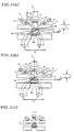
- Figs 1(a), (b) and (c) are explanatory views, displaying one embodiment of an optical switch of the present invention: Fig. 1(a) shows a state in which an optical path-changing portion is separated from a light transmission portion; Fig. 1(b) shows a state in which the optical path-changing portion is in contact with the light transmission portion; and Fig. 1(c) shows a plane facing the optical path-changing portion and a plane corresponding to the optical path-changing portion in the light transmission portion.
- Fig. 2 is an explanatory view schematically showing another embodiment of an optical switch of the present invention.
- Fig. 3 is an explanatory view schematically showing another embodiment of an optical switch of the present invention.
- Fig. 4 is an explanatory view schematically showing another embodiment of an optical switch of the present invention.
- Fig. 5 is an explanatory view schematically showing another embodiment of an optical switch of the present invention.
- Fig. 6 is an explanatory view schematically showing another embodiment of an optical switch of the present invention.
- Fig. 7 is a partially enlarged view schematically showing another embodiment of an optical switch of the present invention.
- Fig. 8 is a partially enlarged view schematically showing another embodiment of an optical switch of the present invention.
- Fig. 9 is an explanatory view schematically showing another embodiment of an optical switch of the present invention.
- Figs. 10(a) and (b) are cross-sectional views schematically showing a modification of an actuator member in an actuator portion constituting an optical switch of the present invention.
- Fig. 10(a) shows an embodiment of a piezoelectric/electrostrictive element using a displacement in Y direction, which is a direction of lamination
- Fig. 10(b) shows an embodiment of a piezoelectric/electrostrictive element using a displacement in X direction, which is a direction perpendicular to a direction of lamination.
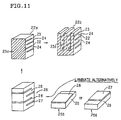
- Fig. 11 is an explanatory view schematically showing an embodiment of a method for producing a laminated piezoelectric/electrostrictive element.
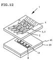
- Fig. 12 is an explanatory view schematically showing one embodiment of a multichannel optical switch of the present invention.
- Fig. 13 is an explanatory view schematically showing another embodiment of a multichannel optical switch of the present invention.
- Fig. 14 is an explanatory view schematically showing another embodiment of a multichannel optical switch of the present invention.
- Fig. 15 is an explanatory view schematically showing another embodiment of a multichannel optical switch of the present invention.
- Fig. 16 is an explanatory view schematically showing another embodiment of a multichannel optical switch of the present invention.
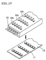
- Fig. 17 is an explanatory view schematically showing another embodiment of a multichannel optical switch of the present invention.
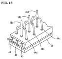
- Fig. 18 is an explanatory view schematically showing another embodiment of a multichannel optical switch of the present invention.
- Fig. 19 is an explanatory view schematically showing another embodiment of a multichannel optical switch of the present invention.
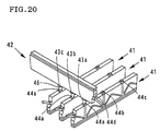
- Fig. 20 is an explanatory view schematically showing another embodiment of a multichannel optical switch of the present invention.
- Fig. 21 is an explanatory view schematically showing another embodiment of a multichannel optical switch of the present invention.
- Fig. 22 is an explanatory view schematically showing another embodiment of a multichannel optical switch of the present invention.
- Figs. 23(a) and 23(b) are explanatory views, displaying another embodiment of an optical switch of the present invention: Fig. 23(a) shows a state in which an optical path-changing portion is separated from a light transmission portion, and Fig. 23(b) shows a state in which the optical path-changing portion is in contact with the light transmission portion.
- Fig. 24 is an explanatory view schematically showing another embodiment of an optical switch of the present invention.
- Fig. 25 is an explanatory view schematically showing another embodiment of a multichannel optical switch of the present invention.
- Fig. 26 is an explanatory view schematically showing still another embodiment of a multichannel optical switch of the present invention.
- Fig. 27 is an explanatory view schematically showing yet another embodiment of a multichannel optical switch of the present invention.
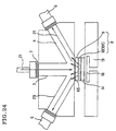
- Fig. 28 is an explanatory view schematically showing yet another embodiment of a multichannel optical switch of the present invention.
- Fig. 29 is an explanatory view schematically showing yet another embodiment of a multichannel optical switch of the present invention.
- Figs 1(a), (b), and (c) are explanatory views schematically showing one embodiment of an optical switch of the present invention: Fig. 1(a) shows a state in which an optical path-changing portion is separated from a light transmission portion, Fig. 1(b) shows a state in which the optical path-changing portion is in contact with the light transmission portion, and Fig. 1(c) shows a plane facing the optical path-changing portion and a plane corresponding to the optical path-changing portion in the light transmission portion.
- Figs. 23(a) and 23(b) are explanatory views schematically showing a state of operation of another embodiment of an optical switch of the present invention.
- an optical path-changing portion 8 is separated from a light transmission portion 1 by displacement of the actuator portion 11.
- Light 21 that is input to an light transmission channel 2 of the light transmission portion 1 is totally reflected at a light reflecting plane 1a of the light transmission portion 1 where a refractive index is adjusted to a predetermined value, without transmitting the light.
- the light is transmitted to one light transmission channel 4 on an output side.
- the actuator portion 11 when the actuator portion 11 is reversed to a non-activation state from this condition, the displacement of the actuator 11 is reset as shown in Fig. 1(b).
- a light introduction member 9 of the optical path-changing portion 8 contacts the light transmission portion 1 at a distance less than a wavelength of light.
- the light 21 input to the light transmission channel 2 is taken to the light introduction member 9 from the light transmission portion 1, and is transmitted through the light introduction member 9.
- the light 21 transmitted through the light introduction member 9 reaches an optical path-changing member 10.
- the light is reflected at a reflecting plane 10a of the optical path-changing member 10 constituted with a light reflector which specularly reflects light (hereinbelow sometimes referred to as "a specular reflector"), and is transmitted to another output-side light transmission channel 5 in a direction different from the direction of the light reflected at the light reflecting plane 10a of the optical path-changing member 10.
- a specular reflector which specularly reflects light
- the optical path-changing member 10 constituted with a light scattering body 10f which scatters light or a light reflector which diffusely reflects light (not illustrated, and hereinbelow sometimes referred to as "a diffuse reflector")
- the light 21 which reached the optical path-changing member 10 changes its optical path in various directions by the light scattering body 10f or the diffuse reflector and emitted outside.
- the light is transmitted to a plurality of output-side light transmission channels 4, 5 simultaneously.
- the optical switch of the present invention shown in Figs. 1(a), 1(b) and Figs. 23(a), 23(b) performs optical switching: the specific light 21 introduced to the light transmission channel 2 of the light transmission portion 1 may be transmitted to different one or more light transmission channels 4, 5 by optionally switching or dividing an optical path based on external signals such as voltage to the actuator portion 11.
- traveling directions of input light or output light may be varied.
- each input light 21 may be reflected at the light reflecting plane 1a of the light transmission portion 1 or the light reflecting plane 10a of the optical path-changing portion 8, and may be transmitted to specific output-side transmission channels 4, 5 for each reflected light thereof.
- an optical switch may be achieved in which great many optical paths may be optionally selected for specific light.
- an optical path-changing portion 8 provided with a light scattering body 10f or a diffuse reflector is prepared according to a use, there is realized an optical switch capable of dividing an optical path of the input light 21 and transmitting the light to a plurality of light transmission channels 4, 5 simultaneously.
- the light transmission channels 4, 5 are switched not by the change in refractive indexes due to physical effects - for instance, electro-optic effects and so forth unique to a material - but by the mechanical operations of contacting or separating the optical path-changing portion 8 from the light transmission portion 1.
- the moving distance of the optical path-changing portion 8 to perform switching is only in a wavelength order of light, so that high-speed switching may be performed.
- switching can be performed with low power consumption.
- optical switching may be basically performed in a closed space and there is no need for switching the light that transmits through the atmosphere, so that attenuation of signals relating to switching may be greatly restrained.
- the light transmission portion 1 in the present invention has the light reflecting plane 1a that is provided at least at one part of a surface 1d facing the optical path-changing portion 8 described below, for reflecting light; and the light transmission channels 2, 4, 5, consisting of an optical wave guiding body, into at least three directions with the light reflecting plane 1a as a starting point.
- the optical switch in which multiple optical paths may be optionally selected for each specific light or the optical switch capable of dividing the optical path for the input light 21 and transmitting the light to a plurality of light transmission channels simultaneously may be provided. Attenuation of signals relating to switching may be restrained to a high degree.
- the light reflecting plane 1a arranged in the light transmission portion 1 of the present invention is required to include a part of the portion 1b corresponding to the optical path-changing portion 8, in a plane 1d facing the optical path-changing portion 8 described below.
- the light reflecting plane 1a may includes a plane other than a portion 1b corresponding to the optical path-changing portion 8.
- the light reflecting plane 1a includes the portion 1b corresponding to the optical path-changing portion 8 in order to switch input light effectively.
- the light reflecting plane 1a arranged in light transmission portion 1 to be a starting point of each of the light transmission channel 2, 4, 5 is required to be designed so as to include a plane where the light 21 input in the light transmission channel 2 project, in the plane 1d of the light transmission portion 1 facing the optical path-changing portion 8 in consideration of disposition of each of the light transmission channels 2, 4, and 5.
- the light transmission channels 2, 4, and 5 provided in the light transmission portion 1 of the present invention may include: for instance, a light transmission portion, as shown in Figs. 1(a), (b), Fig. 2, consists of a single optical wave guiding body and is substantially formed with the light transmission channels 2, 4, 5 toward at least three directions with the light reflecting plane 1a of the light transmission portion 1 as a starting point by providing, at a part of the optical wave guiding body, a plurality of light-signal input ends 43 and/or light-signal output ends 44 having a face roughly orthogonal to the input and output direction of light.
- the light transmission channels 2, 4, 5 are preferably formed by an optical waveguide 1c. If the light transmission channels 2, 4, 5 are formed by an optical waveguide 1c, light could be transmitted in a narrower space and the attenuation of signals that is troublesome in case of long-distance communication, could be reduced to a high degree.
- the optical switch of the present invention may be configured to directly input and output light between optical fibers 6 or the like and the light transmission portion 1 by joining the optical fibers 6 or the like to a plurality of light-signal input ends 43 and/or light-signal output ends 44 of the light transmission portion 1 with an adhesive (not illustrated) or the like.
- the optical switch may be configured to input and output light between optical fibers 6 or the like and the light transmission portion 1 through prisms (not illustrated), by arranging the prisms at a plurality of the light-signal input ends 43 and/or the light-signal output ends 44 of the light transmission portion 1.
- the optical switch it is preferable to configure the optical switch to input and output light between optical fibers 6 or the like and the light transmission portion 1 through lenses 7, by arranging the lenses 7 such as a focusing lens and a collimator lens at a plurality of the light-signal input ends 43 and/or the light-signal output ends 44 of the light transmission portion 1 as shown in Figs. 1(a), (b), (c), Fig. 2, and the like, thus reducing input and output loss due to light divergence.
- the optical switch in which the light transmission channels 2, 4, 5(3) composed of an optical wave guiding body are not restricted to a specific direction as shown in Figs. 1 (a), (b), (c) and Fig. 2, loss due to light divergence at the light transmission portion 1 is reduced.
- the thickness indicated as t in the figures is preferably 1 mm or less, or more preferably 0.5 mm or less.
- the directions of the light transmission channels 2, 4, 5 are properly determined by relations with refractive indexes between the light wave guiding body, constituting the light transmission channels 2, 4, 5, and the open air (generally air), and by relations with reflection angles at the light reflection member 10 of the optical path-changing portion 8 described later.
- the directions of the light transmission channels 2, 4, 5 are properly determined in consideration of a relation of a refractive index between an optical wave guiding body constituting the light transmission channels 2, 4, 5 and the open air (generally air).
- the light transmission channels 2, 4, 5 may extend into directions that are appropriate only in these relations.
- the light transmission channels 2a, 2b, 4a, 4b, 5a, 5b composed of an optical waveguide
- the light transmission channels can be extended without being paralleled as an input-side light transmission channel 2a and another input-side light transmission channel 2b.
- the directions where the transmission channels extend may be changed halfway within a range where light totally reflects in the optical waveguide to form each of the light transmission channels 2a, 2b, 4a, 4b, 5a, 5b by combining straight optical waveguides and non-straight optical waveguides.
- the degree of freedom in the shapes of the light transmission channels 2a, 2b, 4a, 4b, 5a, 5b is high, and smaller optical switches may be realized.
- the optical wave guiding body constituting the light transmission channels 2, 4, 5, in the present invention has refractive indexes to confine introduced light internally and then transmit the light.
- the body may be composed of a material having a single refractive index.
- the body is preferably composed of two or more layers having different refractive indexes since light divergence toward laminated layers may be restrained.
- each light transmission channel 2, 4, 5 is formed of an optical waveguide because the light transmission channels 2, 4, 5 in complex shapes may be easily prepared, the optical waveguide may be easily joined to each other and, in addition to the characteristic of the layered optical wave guiding body, light divergence inside layers is also restrained, so that light may be transmitted with an extremely small loss.
- optical waveguides indicate the ones that are composed of a transparent material having a distribution of different refractive indexes and perform light transmission by confining light internally.
- the optical wave guiding body is, for instance, the one made of glass, quartz, transparent plastic, transparent ceramics, or the like; a laminated body made of multiple layers having different refractive indexes; substrates provided with a coating layer of a transparent material on a surface; or the like.
- the optical waveguide there is exemplified the one having a substrate consisting of glass such as quartz glass and alkali borosilicate glass, insulator crystal such as lithium niobate and yttrium iron garnet, compound semiconductor such as gallium arsenide and indium phosphide, plastic (polymer) such as polymethylmethaacrylate (PMMA) and polyimide, or the like, formed with a film thereon formed of a material having a refractive index changed by doping an impurity and so forth to the common system of material as the substrate; and the one in which a layer or portion having a different refractive index is formed by directly diffusing an impurity and so forth to the aforementioned substrate.
- glass such as quartz glass and alkali borosilicate glass
- insulator crystal such as lithium niobate and yttrium iron garnet
- compound semiconductor such as gallium arsenide and indium phosphide
- plastic (polymer) such as
- the methods of forming a film on a substrate include, for instance, sputtering method, vacuum deposition methods such as molecular beam epitaxy (MBE), chemical vapor deposition (CVD), liquid phase epitaxy (LPE), vapor phase epitaxy (VPE), thermal polymerization used to form a plastic layer, and so forth.
- MBE molecular beam epitaxy
- CVD chemical vapor deposition
- LPE liquid phase epitaxy
- VPE vapor phase epitaxy
- thermal polymerization used to form a plastic layer, and so forth.
- impurity ion implantation impurity ion diffusion
- these methods may be repeated. The number of layers may be appropriately selected based on objects.
- the film or layer formed by the above-noted means has to be patterned to provide predetermined light transmission channels 2, 4, 5.
- the patterning may be performed by, for instance, removing unnecessary portions in photolithography or the like, or by preliminarily setting a masking material on the above-noted substrate and then forming a film or diffusing an impurity to provide predetermined light transmission channels 2, 4, 5.
- the optical path-changing portion 8 of the present invention is provided in proximity to the light reflecting plane 1a of the light transmission portion 1 in a movable condition, and it possesses at least a light reflection member 10 for reflecting or scattering light.
- the optical path of the light 21 of the light transmission channel 2 when the optical path-changing portion 8 is brought into contact with the light transmission portion 1 may be optionally taken out and reflected (specularly reflected or diffusely reflected) or scattered on the optical path-changing member 10 to switch the light 21 to an optical path which is different from the optical path where the light 21 is reflected at the light reflecting plane 1a of the light transmission portion 1 and is transmitted to one light transmission channel 4 or to divide the light 21 to a plurality of light transmission channels 4, 5.
- a compact and highly-integrated multichannel optical switch may be manufactured without any false operation by crosstalk or the like.
- the moving distance of the optical path-changing portion 8 for switching is only in the order of light wavelength, high-speed switching may be performed and an optical path itself does not have to be moved, thus reducing power consumption.
- the optical path-changing portion 8 is arranged from the light reflecting plane 1a of the light transmission portion 1 at a distance longer than a wavelength of input light 21 when the actuator portion 11 is in a non-operable or operable state; and the optical path-changing portion is arranged from the light transmission portion 1 at a distance shorter than a wavelength of input light 21 when the actuator portion 11 is in the reverse condition thereto.
- the optical path-changing portion 8 when the actuator portion 11 is at an operable state, the optical path-changing portion 8 may be arranged from the light reflecting plane 1a of the light transmission portion 1 at a distance longer than a wavelength of input light 21. As shown in Fig. 1(b), when the actuator 11 is in a non-operable state, the optical path-changing portion 8 may be arranged from the light reflecting plane 1a of the light transmission portion 1 at a distance same as a wavelength of input light 21 or shorter. On the contrary, as shown in Fig. 5, the optical path-changing portion 8 may be arranged from the light transmission portion 1 at a distance same as a wavelength of input light 21 or shorter when the actuator portion 11 is in an operable state.
- the optical path-changing portion 8 may be arranged from the light transmission portion 1 at a distance longer than a wavelength of input light 21.
- An optical path-changing portion 8 in the present invention may be provided with a specular reflector 10d shown in Figs. 1(a), 1(b) and the like or a light scattering body 10f shown in Figs. 23(a), 23(b) and the like or a diffuse reflector (not illustrated).
- the optical switch may include an optical path-changing portion 8 provided with the specular reflector 10d as shown in Figs. 1(a), 1(b) and the like in the case that the purpose is to switch a specific optical path to another specific optical path; and the optical switch may include an optical path-changing portion 8 provided with the light scattering body 10f as shown in Figs. 23(a), 23(b) and the like or the diffuse reflector (not illustrated) in the case that the purpose is to divide an optical path to a plurality of other optical paths.
- the specular reflector 10d exhibits total reflection.
- Reflection angles at the specular reflector 10d may be appropriately determined based on the configuration of switches in accordance with the purposes.
- the reflection member may include: for example, a plate optical path-changing member 10 arranged in a flat condition at an angle of 0° as shown in Fig. 9.
- the optical path shown by a broken line in Fig. 9 shows an optical path when the optical path-changing portion 9 is brought into contact with the light transmission portion 8.
- reflection angles of the specular reflector 10d may be the angles, as shown in Figs. 1 (a), (b), and (c), to switch an optical path of light 21 that is input to one light transmission channel 2 and is transmitted to the light transmission channel 4 on an output side, to an optical path of light that is reflected at the specular reflector 10d of the optical path-changing portion 8 and is transmitted to the light transmission channel 5 on another output side.
- the reflection angles of the light reflection member 10 may be the reflection angles, as shown in Fig.
- the specular reflector 10d in the present invention includes, for instance, a plate specular reflector made of a light reflecting material that is arranged with a predetermined inclination, a specular reflector such as a trigonal prism and a rectangular parallelepiped made of a light reflecting material that is arranged with a predetermined inclination, and so forth.
- the specular reflector may also include an electrode 16 having a light reflecting surface as described later and having functions as the specular reflector 10d as shown in Fig. 7.
- the specular reflector 10d may have a substrate 10c of a trigonal prism, rectangular parallelepiped and so forth formed with a light reflecting film 10b.
- the specular reflector 10d as shown in Fig. 6 may be the one having the light reflecting film 10b itself that is formed integrally on the light introduction member 9 of a trigonal prism, a rectangular parallelepiped or the like at the side of a displacement transmission member 12, and so forth.
- the light reflection member 10 having the substrate 10c of a, trigonal prism, rectangular parallelepiped or the like formed with the light reflecting film 10b, as shown in Fig. 5, or a reflector such as a trigonal prism and a rectangular parallelepiped made of a light reflecting material that is arranged with a predetermined inclination is preferable.
- the light reflecting film 10b is formed integrally on the light introduction member 9 of a trigonal prism, a rectangular parallelepiped or the like at the side of the displacement transmission member 12 as shown in Fig. 6 and that the displacement transmission member 12 may be made of an elastic material in the point that the number of components can be reduced, manufacturing costs may be low, and contact precision between the optical path-changing portion 8 and the light transmission portion 1 may improve.
- the light reflecting film 10b is formed on the light introduction member 9 on the side of the displacement transmission member 12 in the optical switch shown in Fig. 6. This is because precision of reflection angles could not be maintained because of the characteristics of the displacement transmission member 12 if the film is formed on the displacement transmission member 12. Accordingly, it is preferable that the light introduction member 9 has a hardness so as not to change the angle of a light reflection member by the operation of the actuator portion 11 in such an optical switch.
- the materials include, for instance, single metal, alloy, glass, ceramics, rubber, organic resin and so forth by itself or the combination of two or more kinds thereof.
- the single metal and the components of the alloy include aluminum, titanium, chromium, iron, cobalt, nickel, silver, copper, tin, tantalum, tungsten, iridium, platinum, lead, and so forth.
- the light reflection member 10 may contain two or more kinds of the materials uniformly, but may also be a layered member, each of the layers consisting of a material different from the others. Additionally, the optical path-changing member 10, as a whole, may consist of the materials. As shown in Fig. 6, the member may be one formed with the light reflecting film 10b on the surface.
- the light reflecting film 10b there may be employed, for instance, thin film forming methods such as a vacuum deposition method, a sputtering method, a plating method, an ion plating method, an ion beam method, or a CVD method.
- thin film forming methods such as a vacuum deposition method, a sputtering method, a plating method, an ion plating method, an ion beam method, or a CVD method.
- an optical switch where an optical path-changing portion 8 as shown in Fig. 23 is provided with a light scattering body 10f or a diffuse reflector (not illustrated), an angle of the surface is out of the question basically, and the light scattering body 10f or a diffuse reflector may be disposed in a position where a loss of scattering light 65 or diffuse reflection light is small from a positional relation with each of the light transmission channels 2, 3 and 4.
- a diffuse reflector in the present invention may have the same structure basically as the aforementioned specular reflector and have a roughened reflecting surface.
- the roughening may be within a suitable range in consideration of a wavelength of light to be transmitted, and a general method of roughening may be employed as a method of the roughening.
- a light scattering body 10d in the present invention may be prepared by dispersing, for example, a ceramic powder of zirconia, titania or the like, a metal oxide powder of lead oxide or the like, a mixture powder thereof, or the like, in, for example, an epoxy, acrylic, or silicone transparent resin in view of emission efficiency and maintaining flatness.
- the light scattering body 10d preferably includes 10 - 100 mass parts of a ceramic powder, a metal oxide powder, or a mixture thereof relative to 100 mass parts of the transparent resin.
- the whole optical path-changing portion is constituted with the light scattering body 10f
- 10 - 100 mass parts of a glass powder having an average particle size of 0.5 - 10 ⁇ m is further mixed with the composition relative to 100 mass parts of a ceramic powder. If a light scattering body 10d has such a composition, contact ability and separating ability with a light transmission portion are improved.
- a light introduction member 9 is not always necessary, and in, for example, an optical switch where an optical path-changing portion 8 as shown in Figs. 23(a) and 23(b) is provided with a light scattering body 10f or a diffuse reflector (not illustrated), the optical path-changing portion 8 may be constituted only by the light scattering body 10f or the diffuse reflector and have a structure that the light scattering body 10f or the diffuse reflector is brought into direct contact with the light transmission portion.
- a light introduction member 9 of a transparent material is disposed on the specular reflector 10d in the point that a contact ability between the optical path-changing portion 8 and the light transmission portion 1 can be optimized by specializing a light introduction function and an optical path-changing function.
- an optical path-changing portion 8 is provided with a light scattering body 10f or a diffuse reflector (not illustrated)
- a light introduction member 9 of a transparent material on the light scattering body 10f or the diffuse reflector as shown in Fig. 24 in the similar point as in the optical switch provided with a specular reflector.
- an optical switch where an optical path-changing portion 8 is provided with a light scattering body 10f or a diffuse reflector (not illustrated), in the case that light is input almost perpendicularly to a reflecting plane 1a of the light transmission portion 1 from the light transmission channel 3, the input light 21 is divided to transmitted to the light transmission path 29 and 4 which are divided right and left with the light transmission channel 3 being located therebetween.
- a material of the light introduction member 9 is preferably a transparent material: the material has a smaller difference in refractive indexes with the light transmission portion 1 than the difference in refractive indexes between the light transmission portion 1 and the open air (generally air), so as to take out the light from the light transmission portion 1 and return the light to the light transmission channels 4, 5 of the light transmission portion 1 when the optical path-changing portion 8 is in contact with the light transmission portion 1.
- a transparent material having roughly the same light refractive index as the light transmission portion 1 is more preferable.
- a material to give such quality may include, for instance, glass, quartz, transparent plastic, transparent resin, transparent ceramics, and so forth.
- the light introduction member 9 may also be entirely or partially composed of transparent liquid by providing the transparent liquid between the optical path-changing member 10 or the light introduction member 9 and the light transmission portion 1.
- the transparent liquid effectively fills up a gap between the optical path-changing member 10 or the light introduction member 9 and the light transmission portion 1, so that optical paths may be easily altered.
- a transparent liquid includes there may be employed, for instance, organic solvents of low vapor pressure, oil, and so forth.
- a transparent liquid may be selected in consideration of a difference in refractive index between the liquid and the light transmission portion 1 and between the liquid and the light introduction member 9.
- a method of holding fluid transparent liquid on the optical path-changing portion for example, a conventional art in which a wall in an appropriate height is provided at an upper outer periphery of the optical path-changing portion 8, and so forth may be adapted.
- a method is preferable in which the light introduction member 9 is formed with recessed and protruded parts or porous parts, and transparent solution is held in a capillary phenomenon by impregnating transparent solution thereto.
- volatile transparent liquid is used as a transparent liquid, it is preferable to adapt a configuration in which the optical path-changing portion 8 is sealed airtight with the light transmission portion 1 to avoid vaporization.
- the area where the light introduction member 9 is in contact with the light reflecting plane 1a of the light transmission portion 1 determines the amount of light taken out to the optical path-changing member 10.
- a surface 9a of the light introduction member facing the light transmission portion 1 is preferably made wider with including a whole plane where the light 21 input in the light transmission channel 2 projects.
- the surface 9a facing the light reflecting plane 1a of the light transmission portion 1 is flat so as to secure the surface for a contact area with the light transmission portion 1.
- the flatness is preferably 1 ⁇ m or less, more preferably 0.5 ⁇ m or less, and further preferably 0.1 ⁇ m or less.
- the flatness of the surface 9a facing the light reflecting plane 1a of the light transmission portion 1 is important in order to reduce a gap under the condition where the light introduction member 9 is in contact with the light reflecting plane 1a of the light transmission portion 1.
- the flatness is not necessarily limited to the one mentioned above as long as the contact part deforms in the contacting state. However, it is preferable that the flatness is small enough in comparison with a displacement of the actuator portion 11.
- the flatness of the surface 9a of the light introduction member 9 is preferably 0.005 ⁇ m or more, and more preferably 0.015 ⁇ m or more so that separation may be securely performed when the light introduction member 9 in contact with the light reflecting plane 1a of the light transmission portion 1 is separated.
- flatness described here includes both surface roughness and undulation.
- the thickness of the light introduction member 9 is preferably less than 50 ⁇ m, more preferably less than 20 ⁇ m, so as to reduce the loss of light.
- the actuator portion 11 in the present invention has functions of displacing with external signals and of transmitting the displacement to the above-noted optical path-changing portion 8, thus allowing the switching by mechanical operations, such as contacting or separating (off-contacting) the portion from the light transmission portion.
- the actuator portion 11 may be, for instance, one that generates displacement by an elastic body such as a plate spring. However, in view of excellent controllability and high-speed responsiveness, the actuator portion is preferable that has a displacement transmission portion 12, a piezoelectric/electro-strictive element 14, a vibrating member 18 and a fixing member 19, depending on the need. This type of the actuator portion 11 will be explained in detail below for each component.
- the displacement transmission member 12 in the present invention is arranged between the optical path-changing portion 8 and the piezoelectric/electrostrictive element 14, based on the need.
- the member is arranged in order to transmit displacement of the piezoelectric/electrostrictive element 14 to the optical path-changing portion 8 and to set a contact area between the optical path-changing portion 8 and the light transmission portion 1 at a predetermined size.
- a type of piezoelectric/electrostrictive element 14 generating bending displacement shown in Figs. 1, Fig. 5, or the like is extremely effective in averaging the amount of displacement distributed within the piezoelectric/electrostrictive element 14 and contacting or separating a whole surface of the optical path-changing portion 8 evenly from the light transmission portion 1.
- the displacement transmission member 12 preferably has a configuration where the member may be in contact with both optical path-changing portion 8 and the piezoelectric/electro-strictive element 14 in a large area to allow effective transmission of displacement of the piezoelectric/electrostrictive element 14 to the optical path-changing portion 8.
- a material of the displacement transmission member 12 preferably has a hardness to allow direct transmission of displacement of the piezoelectric/electrostrictive element 14 to the optical path-changing portion 8.
- materials having such quality there may be employed, for instance, rubber, organic resin, organic adhesive film, glass, and so forth.
- organic resin made of an epoxy-based, acrylic-based, silicone-based, polyolefine-based or the like organic material, or organic adhesive films are preferable.
- Organic resin or organic adhesive films in which curing and shrinkage are restrained by mixing a filler into these organic materials, are more preferable.
- the displacement transmission member 12 is arranged by laminating the displacement transmission member 12 onto the piezoelectric/electrostrictive element 14.
- the method for lamination may be, for instance, a method of lamination with an adhesive, a method of coating the above-noted material of the displacement transmission member as solution, paste or slurry onto the piezoelectric/electrostrictive element 14, a method of bonding an organic adhesive film by heating, and so forth. Since an adhesive is unnecessary, the method of bonding an organic adhesive film by heating is preferable.
- a plate member 13 is further disposed on the displacement transmission member 12 as shown in Fig. 8 in consideration of maintaining the reflection angle of the optical path-changing member 10 at a predetermined one.
- a material of the plate member 13 in order to maintain flatness of the plate member 13, a material in which ceramic powder such as alumina, zirconia, titania, glass or the mixture thereof is dispersed in epoxy-based, acrylic-based, silicone-based or the like organic resin, is preferable. In this case, it is preferable to have ceramic powder dispersed therein at 10 to 100 mass parts relative to 100 mass parts of organic resin.
- the displacement transmission member 12 is not necessarily required. As shown in Fig. 7, displacement of the piezoelectric/electrostrictive element 14 may be directly transmitted to the light introduction member 9 without providing the displacement transmission member between the piezoelectric/electrostrictive element 14 and the optical path-changing portion 8.
- the piezoelectric/electrostrictive element 14 in the present invention has a piezoelectric/electrostrictive layer 15, and at least one pair of electrodes 16, 17 arranged on at least one part of the piezoelectric/electrostrictive layer 15.
- piezoelectric/electrostrictive means piezoelectric and/or electrostrictive.
- the piezoelectric/electrostrictive element 14 generates displacement by the application of voltage to the electrodes 16, 17.
- An element that achieves displacement in the thickness direction of the piezoelectric/electrostrictive layer 15, is preferable in the point that displacement of the piezoelectric/electrostrictive element 14 may be transmitted as is, as displacement or vibrations in the direction of the light transmission portion 1, to an optical path-changing portion 8.
- the piezoelectric/electrostrictive element 14 may have a structure of having one piezoelectric/electrostrictive layer 15, or a structure of having multi-layered piezoelectric/electrostrictive layers 15 of two, three or more layers.
- the structure has a multi-layered piezoelectric/electrostrictive layers 15, it is generally enough to dispose a pair of electrodes 16, 17 in every piezoelectric/electrostrictive layer 15.
- the piezoelectric/electrostrictive element 14 may have a so-called laminated (stacked) piezoelectric/electrostrictive element, where each piezoelectric/electrostrictive layer 15 and each electrode 16, 17 are laminated alternately.
- piezoelectric ceramics are preferable.
- the material may be electrostrictive ceramics, ferroelectric ceramics or antiferroelectric ceramics, and so forth.
- the material may either require polarization or not.
- the material is not limited to ceramics, and may be a piezoelectric material consisting of polymer such as PVDF (polyvinylidene fluoride) and so forth, or a complex of the polymer and ceramics.
- piezoelectric ceramics or electrostrictive ceramics may include one of lead zirconate, lead titanate, lead magnesium niobate, lead nickel niobate, lead zinc niobate, lead manganese niobate, lead antimony stannate, lead manganese tungstate, lead cobalt niobate, barium titanate, sodium bismuth titanate, bismuth neodymiumtitanate (BNT system), potassium sodium niobate, strontium bismuth tantalate, and so forth singly, as a mixture, or as a solid solution thereof.
- lead zirconate lead titanate
- lead magnesium niobate lead nickel niobate
- lead zinc niobate lead manganese niobate
- lead antimony stannate lead manganese tungstate
- lead cobalt niobate barium titanate, sodium bismuth titanate, bismuth neody
- Ceramics are preferably a main component at 50 wt.% or more in the ceramic components constituting a piezoelectric/electrostrictive body.
- Particularly preferable materials are materials containing lead zirconate titanate (PZT system) as the main component, material containing lead magnesium niobate (PMN system) as the main component, material containing lead nickel niobate (PNN system) as the main component, materials containing a mixture or a solid solution of lead zirconate, lead titanate, and lead magnesium niobate as the main component, materials containing a mixture or a solid solution of lead zirconate, lead titanate, and lead nickel niobate as the main component, and materials containing sodium bismuth titanate as the main component in view of having high electromechanical coupling factor and piezoelectric/electrostrictive constant number and being easily capable of obtaining one having a stable material composition.
- PZT system lead zirconate titanate
- PMN system lead magnesium
- ceramics further containing one or more oxides of lanthanum, calcium, strontium, molybdenum, tungsten, barium, niobium, zinc, nickel, manganese, cerium, cadmium, chromium, cobalt, antimony, iron, yttrium, tantalum, lithium, bismuth, tin, and so forth.
- lanthanum calcium, strontium, molybdenum, tungsten, barium, niobium, zinc, nickel, manganese, cerium, cadmium, chromium, cobalt, antimony, iron, yttrium, tantalum, lithium, bismuth, tin, and so forth.
- lanthanum and/or strontium is added to lanthanum and/or strontium, which sometimes enables adjustment of coercive electric field or piezoelectric properties.
- preferable ceramics are: ceramics that have lead zirconate as a main component; ceramics that have a component consisting of a mixture or a solid solution of lead zirconate and lead stannate as a main component; ceramics that have lead zirconate as a main component with lanthanum oxide added thereto; and ceramics that have a mixture or a solid solution of lead zirconate and lead stannate as a main component with lead niobate added thereto.
- the thickness of the piezoelectric/electrostrictive layer 15 is preferably 5 to 100 ⁇ m, more preferably 5 to 50 ⁇ m, and further preferably 5 to 30 ⁇ m. Moreover, the piezoelectric/electro-strictive layer 15 may be either dense or porous. When the layer is porous, the porosity is preferably less than 40%.
- the electrodes 16, 17 may include: as shown in Figs. 1, Fig. 8 and so forth, the first electrode 16 formed on at least one part of a surface of the piezoelectric/electrostrictive layer 15 on the side of the optical path-changing portion 8, and the second electrode 17 formed at least one part of a surface of the piezoelectric/electrostrictive layer 15 on the side of the substrate 20 as mentioned above; first and second electrodes 16, 17 formed in a comb shape on either or both surfaces of the piezoelectric/electrostrictive layer 15 on the side of the optical path-changing portion 8 or the substrate 20 as shown in Fig. 9 (Fig. 9 showing an optical switch formed on a surface on the side of the optical path-changing portion 8); and so forth.
- a conductive metal that is generally solid at room temperature is employed. It is preferable to employ, for example, a single metal or alloy of two or more kinds selected from aluminum, titanium, chromium, iron, cobalt, nickel, copper, zinc, niobium, molybdenum, ruthenium, palladium, rhodium, silver, tin, tantalum, tungsten, iridium, platinum, gold, lead and so forth, or a combination of two or more systems thereof.
- the material may be a mixture of these materials and aluminum oxide, zirconium oxide, silicon oxide, glass, a piezoelectric/electrostrictive material or the like, or a cermet thereof.
- a material containing a platinum group metal such as platinum, rhodium and palladium is preferable among the materials since the metal has resistance under a high-temperature oxide atmosphere during the heat treatment of the piezoelectric/electrostrictive layer 15.
- An electrode material is more preferable that has a platinum group metal such as platinum, rhodium and palladium, or an alloy containing the platinum group metal such as silver-platinum, platinum-palladium and platinum-silver-palladium as a main component.
- a metal having low melting point such as aluminum, gold, or silver.
- both the first electrode 16 and the second electrode 17 are formed on a surface of the piezoelectric/electrostrictive layer 15 on the side of the optical path-changing portion 8 or the substrate 20 as shown in Fig. 9, it is preferable to form both the first electrode 16 and the second electrode 17 with the same material.
- the electrodes 16, 17 may have an appropriate thickness, depending on the purposes, but preferably 0.1 to 50 ⁇ m in thickness.
- a method of forming the piezoelectric/electrostrictive element 14 on the vibrating member 18 may include: (1) a method of forming a precursor of the piezoelectric/electro-strictive layer 15 by a press molding method with a mold or a tape forming method with slurry materials and so forth; preliminarily forming the electrodes 16, 17 on the precursor of the piezoelectric/electrostrictive layer 15 by a film forming method; thermo-compression bonding the precursor of the piezoelectric/electrostrictive layer 15 and the electrodes 16, 17 to the vibrating member 18; and co-firing the precursor of the piezoelectric/electrostrictive layer 15, the electrodes 16, 17 and the unfired vibrating member 18; (2) a method of forming a precursor of the piezoelectric/electrostrictive layer 15 by a press molding method with a mold or a tape forming method with slurry materials and so forth; preliminarily forming the electrodes 16, 17 on the precursor of the
- the word “precursor” here means a thing which has a material constituting a piezoelectric/electrostrictive layer 15 as the main component and which becomes a piezo-electric/electrostrictive body by a thermal treatment or being fired.
- the word “precursor” for an electrode or the like, which is described later, likewise means a thing which becomes an electrode or the like by a thermal treatment or the like.
- a film forming method there may be employed, for example, thick film methods such as screen printing, dipping, electrophoresis, spraying or coating; or thin film methods such as ion beam, sputtering, vacuum deposition, ion plating, chemical vapor deposition (CVD) and plating; and so forth.
- thick film methods such as screen printing are preferable.
- the thick film methods such as screen printing have advantages: leads to electrodes and terminal pads may be simultaneously formed and, additionally, the piezoelectric/electrostrictive layer 15 may be formed by using paste or slurry having ceramic particles as a main component, so that preferable piezoelectric characteristics may be obtained; and the piezoelectric/electrostrictive element 14 and the vibrating member 18 may be joined integrally without using an adhesive, so that the methods are highly reliable and reproducible and, furthermore, they may be easily integrated.
- predetermined patterns may be formed by screen printing, photolithography, and so forth. Patterns may be formed by removing unnecessary parts by machining such as laser beam machining, slicing and ultrasonic machining. However, in accordance with industrial viewpoints, screen printing is preferable. Additionally, the electrodes 16, 17 may be formed by a method of forming electrodes through a through-hole 46 as shown in Fig. 8.
- Firing temperature of the films may be properly determined, depending on the materials thereof, but the temperature is generally 500 to 1400°C. Particularly, for the piezoelectric/electrostrictive layer 15, 1000 to 1400°C is preferable. Additionally, it is preferable to fire the piezoelectric/electrostrictive layer 15 in the presence of a source of vaporization which controls vapor pressure of components constituting the piezoelectric/electrostrictive layer.
- any shape may be adapted for the piezoelectric/electrostrictive layer 15, the first electrode 16 and the second electrode 17, depending on the purposes.
- the shapes may include, for instance, polygons such as a triangle and square, curves such as a circle, ellipse and ring, comb shapes, lattice shapes, or the combination thereof.
- the piezoelectric/electrostrictive layer 15, the first electrode 16, and the second electrode 17 formed on the substrate 20 may be formed integrally with the substrate 20 treating each of the layers 17, 15, and 16 with heat every time after formation of each of the layers 17, 15, and 16 as described above. Alternatively, after forming all the layers 17, 15, and 16, these layers 17, 15, and 16 may be simultaneously treated with heat to integrate them with the substrate 20. Additionally, in case of forming the first electrode 16 and the second electrode 17 by a thin film method, heat treatment is not always necessary to integrate these electrodes.
- this piezoelectric/electrostrictive element 34 is a laminate: an anode layer 22 in which a plurality of layers functioning as anodes are linked, and a cathode layer 23 in which a plurality of layers functioning as cathodes are linked, are both alternately laminated with the piezoelectric/electro-strictive layer 24 therebetween.
- the piezoelectric/electrostrictive element 34 can utilize displacement in Y direction, which is a direction of lamination, and in X direction, which is a direction perpendicular to the direction of lamination.
- Y direction which is a direction of lamination
- X direction which is a direction perpendicular to the direction of lamination.
- direction Z of displacement is Y direction, which is a direction of lamination
- the amount of displacement is a total of displacements in a thickness direction of each piezoelectric/electrostrictive layer.
- the piezoelectric/electrostrictive element 34 is preferably longer in X direction, which is a direction perpendicular to the direction of lamination, than in Y direction, which is a direction of lamination.
- the amount of displacement becomes a displacement in proportion with the length of each piezoelectric layer 21 in X direction.
- a precursor 25 of a piezoelectric/electrostrictive layer is formed by the press molding method or tape forming method with slurry materials and so forth mentioned above.
- precursors 27 and 28 of electrode layers each having predetermined pattern are formed by a film-forming method such as screen printing to obtain complex precursors 255 and 256.
- these complex precursors 255 and 256 are subjected to alternate lamination and compression bonding to obtain a laminated body 26 having a predetermined number of each layers. Then, the laminated body 26 is fired.
- the fired laminated body 26 is cut to expose each of the electrode layers 22 and 23 to one of the two surfaces in parallel with the direction of lamination and facing each other.
- each of joint layers 22a and 23a is formed on each of the surface where each of the electrode layers 22 and 23 are exposed by the aforementioned film-forming method such as screen printing.
- the joint layers 22a and 23a are fired and each of the electrode layers 22, which functions as an anode, is joined with other electrode layers 22, and each of the electrode layers 23, which functions as a cathode, is joined with other electrode layers 23 to obtain a laminated piezoelectric/electrostrictive element 34.
- the thus obtained laminated piezoelectric/ electrostrictive element 34 is preferably cut in a direction of lamination so that portions to serve as a common fixing member 19 are left at constant intervals.
- a plurality of laminated piezoelectric/electrostrictive elements 34 can easily be produced on the same fixing member 19.
- the fixing member 19 can be commonly used, and the vibrating member 18 is not always necessary. Therefore, reducing the number of switch parts can be tried.
- the laminated body 26 may be formed by screen printing besides press molding method, tape forming method, or the like.
- the electrode layers 22 and 23 constituting a part of the piezoelectric/electrostrictive element 34 are of metal having, in particular, resistance in an oxidizing atmosphere at high temperature of the case that the electrode layers are subjected to a heat treatment simultaneously with or at about the same temperature as that for firing of the piezoelectric/electrostrictive layer 24.
- the cutting process where these electrode layers 22 and 23 are exposed may performed to the laminated body 26 before being fired.
- the joint layers 22a and 23a formed after firing the laminated body 26 may be formed with a material different from that of the electrode layers 22 and 23.
- the method for producing the laminated piezoelectric/electrostrictive element 34 is similar to that of a general piezoelectric/electrostrictive element except for the aforementioned matters, and description for such matters is omitted here.
- the vibrating member 18 in the present invention is in contact with at least one part of the piezoelectric/electrostrictive element 14 to support piezoelectric/electrostrictive element 14, and converts strain of a piezoelectric/electrostrictive layer into bending displacement or vibrations.
- the vibrating member 18 is preferably in a plate shape since this is a shape that is likely to vibrate into the direction of the light transmission portion 1.
- the thickness of the vibrating member 18 is preferably the same dimension as the thickness of the piezoelectric/electrostrictive layer 15 described above.
- the vibrating member 18 is likely to follow sintering shrinkage of the piezoelectric/electrostrictive layer 15, so that stress at an interface between the piezoelectric/electrostrictive layer 15 or the electrode layers 16, 17 and the vibrating member 18 decreases and the layer and the member may be easily integrated.
- the member is preferably in the thickness of 1 to 100 ⁇ m, more preferably in the thickness of 3 to 50 ⁇ m, and further preferably in the thickness of 5 to 20 ⁇ m.
- a ratio of thickness in comparison with the piezoelectric/electrostrictive layer 15 is preferably 1:0.5 to 1:10, and more preferably 1:1 to 1:5.
- the vibrating member 18 directly supports the piezoelectric/electrostrictive element 14 without a material such as an inorganic or organic adhesive in consideration of degeneration with the passage of time, heat resistance and weather resistance.
- a material of the vibrating member 18 is highly heat resistant in order to prevent the vibrating member 18 from degenerating during forming the piezoelectric/electrostrictive layer 15 or the like.
- the vibrating member 18 preferably consists of an electric insulating material to maintain an electrical separation of the electrodes 16, 17 and so forth when the electrodes 16, 17 of the piezoelectric/electrostrictive element 14 directly supported thereby, and leads and lead terminals that are connected thereto, etc. are formed on a surface of the vibrating member 18.
- the member consisting of a highly heat resistant metal or porcelain enamel or the like in which a surface of the metal is coated with ceramics such as glass, or the member consisting of ceramics or the like may be employed.
- the member consisting of ceramics is preferable.
- Ceramics constituting the vibrating member 18 may include, for example, stabilized zirconium oxide, aluminum oxide, magnesium oxide, mullite, aluminum nitride, silicon nitride, glass, and so forth.
- stabilized zirconium oxide is preferable since it has high mechanical strength, toughness and little chemical reaction to a piezoelectric/electrostrictive layer and electrodes.
- stabilized zirconium oxide is preferable to be it contained aluminum oxide at 0.1 to 5 mole %.
- the stabilized zirconium oxide includes stabilized zirconium oxide and partially stabilized zirconium oxide.
- the stabilized zirconium oxide is distinguished from zirconium oxide that often generates cracks during a phase transformation between monoclinic crystals and tetragonal crystals at around 1000 °C, since it has a cubic crystal structure or the like and does not generate the phase transformation.
- the stabilized zirconium oxide may include ones that contain a stabilizer such as calcium oxide, magnesium oxide, yttrium oxide, scandium oxide, ytterbium oxide, cerium oxide or rare earth metal oxides at 1 to 30 mole %.
- a stabilizer such as calcium oxide, magnesium oxide, yttrium oxide, scandium oxide, ytterbium oxide, cerium oxide or rare earth metal oxides at 1 to 30 mole %.
- yttrium oxide is preferably contained at 1.5 to 6 mole %, or more preferably 2 to 4 mole %.
- a crystal phase of ceramics constituting the vibrating member 18 may be a mixed phase of cubic crystals and monoclinic crystals, a mixed phase of tetragonal crystals and monoclinic crystals, a mixed phase of cubic crystals, tetragonal crystals and monoclinic crystals, and so forth.
- a tetragonal crystal phase, or a mixed phase of tetragonal crystals and cubic crystals is preferable in consideration of strength, toughness and durability.
- the member is composed of a plurality of crystal grains.
- the average size of the crystal grains is preferably 0.05 to 2 ⁇ m, or more preferably 0.1 to 1 ⁇ m, to improve the mechanical strength of the vibrating member 18.
- the fixing member 19 in the present invention fixes at least one part of the vibrating member 18 so as to vibrate the vibrating member 18.
- the fixing member 19 preferably consists of ceramics, but may be the same or different ceramics from the material of the vibrating member 18.
- ceramics such as stabilized zirconium oxide, aluminum oxide, magnesium oxide, titanium oxide, mullite, spinel, aluminum nitride, silicon nitride, glass, or the like.
- a ceramic material having zirconium oxide as a main component, a ceramic material having aluminum oxide as a main component, or a ceramic material having a mixture thereof is more preferable.
- a component that is likely to be vitrified such as silicon oxide and boron oxide
- An excessive amount of a component that is likely to be vitrified is advantageous in joining to the piezoelectric/electrostrictive element 14.
- it becomes difficult to maintain a composition of a predetermined piezoelectric/electrostrictive layer because of promotion of reaction between the vibrating member 18 and a piezoelectric/electrostrictive layer upon being fired, thus resulting in the decrease in element characteristics.
- the vibrating member 18 and the fixing member 19 are integrated to constitute the substrate 20 consisting of ceramics. Furthermore, a recessed portion 20a shown in Figs. 1 and the like or a hollow portion 20b shown in Fig. 2 and the like (hereinbelow sometimes referred to as recessed portion 20a and the like for convenience of explanation) is preferably formed with giving the vibrating member 18 a thin structure. However, it is not necessarily required to constitute the vibrating member 18 and the fixing member 19 integrally.
- the fixing member 19 made of a metal, for instance, stainless steel, iron and so forth, may fix the vibrating member 18 made of ceramics. In this case, there may be employed a method where a surface of the vibrating member 18 is metallized and the obtained metallized layer is joined to the fixing member 19 by brazing, or the like.
- the substrate is preferably constituted with a material having the same component as a piezoelectric/electrostrictive layer. It is more preferable that the substrate has the same component and the same composition. A substrate of such a material can easily be bonded unitarily with a piezoelectric/electrostrictive layer.
- the recessed portion 20a may be, for instance, circular, elliptic, or polygonal such as square and rectangular, or the combination thereof. However, in case of a polygonal shape, the corners are preferably trimmed in a round ridge.
- the thickness is generally determined according to an object of use of the hollow portion, it is preferable that it is thin without having higher thickness than it needs for functioning of the actuator portion. Particularly when it is constituted as a hollow portion, the thickness is preferable about the size of a displacement of an actuator portion to be used.
- the hollow portion 20b preferably has a thickness of 3 - 50 ⁇ m, more preferably 3 - 20 ⁇ m.
- a method of forming the substrate 20 by sintering the vibrating member 18 and the fixing member 19 for integration a method of laminating layers such as a green sheet or a green tape by thermo compression bonding and subsequently sintering the layers, or the like, may be employed.
- a method of forming the recessed portion 20a or the like with giving the vibrating member 18 a thin structure may be: a method of preliminarily providing a through-hole in a predetermined shape so as to form the recessed portion 20a or the like in a second layer before lamination in case of laminating, for instance, two green sheets or green tapes; a method of providing the recessed portion 20a by machining such as grinding, laser machining, punching by press machining, etc., in a molded body obtained by pressure molding with a mold, casting, injection and so forth; or the like.
- the light transmission portion 1 and the substrate 20 are fixed with a distance between the light transmission portion 1 and the optical path-changing portion 8 by arranging a clearance forming member 45 on the substrate 20 as shown in Fig. 12.
- the clearance forming member 45 may be formed on an entire surface of the substrate 20, except for a region where the piezoelectric/electrostrictive element 14 is arranged.
- the member is preferably formed in patterns so as to equalize a distance between the light transmission portion 1 and the optical path-changing portion 8.
- the optical switch in the present invention may contact or separate (off-contact) a single optical path-changing portion 8 from the light transmission portion 1 by displacement of a single actuator portion 11 described above, but the switch may contact or separate a single optical path-changing portion 8 from the light transmission portion 1 by displacement of a plurality of the actuators 11.
- a multichannel optical switch is a multichannel optical switch provided with a plurality of optical switches each comprising at least a light transmission portion, an optical path-changing portion and an actuator portion; characterized in that the light transmission portion has a light reflecting plane provided on at least one part of a plane facing the optical path-changing portion to totally reflect light, and light transmission channels having optical wave guiding bodies and being provided in at least three directions with the light reflecting plane as a starting point; the optical path-changing portion is provided in proximity to the light reflecting plane of the light transmission portion in a movable condition and has an optical path-changing member for at least reflecting or scattering light; and the actuator portion has a mechanism that is displaced by external signals and transmits the displacement to the optical path-changing portion; and wherein the switching or dividing of an optical path is carried out by contacting or separating the optical path-changing portion to or from the light reflecting plane of the light transmission portion by displacement of the actuator portion in response to the external signals; so as to totally reflect an input light from the light transmission channels at the light reflecting plane
- Each component of the multichannel optical switch in the present invention is the same as those already mentioned for the optical switches. Accordingly, the description of each component is omitted herein, and specific embodiments of multichanneling will be shown.
- multichannel indicates that there are a plurality of locations where optical switching is performed by switching an optical path between a light reflecting plane of the aforementioned light transmission portion and a light reflection member of an optical path-changing portion.
- the so-called “multichannel optical switch” herein includes the ones in which each component is shared between optical switches.
- One embodiment in the present invention may include a multichannel optical switch in which a plurality of optical switches shown in, for instance, Figs . 1 to Fig. 3 are arranged in a row as in Fig. 12.
- the multichannel optical switch performs optical switching in which an optical path of the light input to one input-side light transmission channel 2 is optionally switched and the light is transmitted to two or more output-side light transmission channels 4, 5.
- the multichannel optical switch performs optical switching in which an optical path of each light input to two or more input-side light transmission channels 2, 3 is optionally switched and the light is transmitted to one output-side light transmission channel 4.
- Such a multichannel optical switch has advantages in that the structure is simple and multichanneling is easy.
- An input side and an output side are distinguished simply in relation to the traveling direction of light. Even in the same configuration, input and output are differently termed by reversing a traveling direction.
- Another embodiment in the present invention may include a multichannel optical switch formed with each light transmission channel 2a to 2c, 4a to 4c, 5a to 5c in a plurality of optical switches in a single light transmission portion 1 as shown in Fig. 13. It is preferable that each light transmission channel 2a to 2c, 4a to 4c, 5a to 5c, is formed at an optical waveguide since the light transmission channels 2a to 2c, 4a to 4c, 5a to 5c can be mutually arranged in proximity in such a multichannel optical switch. Also, each light transmission channel in a plurality of optical switches is mutually crossed so as to share a part of each light transmission channel 2a to 2c, 4a to 4c, 5a to 5c, thus greatly miniaturizing and integrating an optical switch.
- another embodiment in the present invention may be a multichannel optical switch in which a plurality of optical switches 51 are constituted by a plurality of optical switch having one input channel 2a to 2c and a plurality of output channels 4a to 4c, 5a to 5c, and one output channel 4a, 4b, 4c is linked with an input channel 2a, 2b, 2c respectively between adjacent optical switches 51, to perform switching the light input from input end portion of one optical switch in each optical path-changing portion of a plurality of optical switches including the optical switch.
- the multichannel optical switch shown in Fig. 14 has an advantage in that signal loss is small in light transmission since light transmission channels 2a, 2b, 2c, 4a, 4b, 4c are composed of an optical waveguide.
- the multichannel optical switch shown in Fig. 15 has an advantage in that design is simple since the light transmission portion as a whole is composed of an optical wave guiding body of the same material (the optical waveguide is excluded) and, in an essential sense, specific light transmission channels 2a to 2c, 4a to 4c, 5a to 5c are formed.
- an optical path of the light input from an input end 43 is switched at each optical path-changing portion 8a, 8b, 8c (not shown in Fig. 15) of a plurality of optical switches.
- the light is emitted from an output end 44a, 44b, 44c and transmitted to an external signal channel.
- another embodiment in the present invention may be a multichannel optical switch where a plurality of optical switches 51 join one output channel 4a, 4b with input channel 2b, 2c, respectively, between adjacent optical switches 51 by an optical fiber 6 to perform switching of light input from input end of at least one optical switch in an optical path-changing portion of a plurality of optical switches.
- the multichannel optical switch similarly to the multichannel optical switch shown in Fig. 15, since the light transmission portion as a whole can be composed of an optical wave guiding body of the same material (the optical waveguide is excluded), it is easily designed. In addition, since optical transmission is performed with an optical fiber, the multichannel optical switch is more advantageous in suppressing divergence of light in comparison to that shown in Fig. 15.
- the multichannel optical switch it is preferable to unitarily form the light transmission portion 1 of each optical switch 51 in view of simplifying the design.
- the multichannel optical switch may be the one in which each optical transmission portion 1 of the optical switches 51 is independently formed.
- another embodiment in the present invention may include a multichannel optical switch in which a plurality of the multichannel optical switches shown in Figs. 14 to 16 described above are arranged in a row as shown in Fig. 17.
- This multichannel optical switch has an advantage in that a large-scale multichanneled optical switch may be easily manufactured since a plurality of light-signal input ends and/or light-signal output ends may be easily provided, and the size is easily reduced since the configuration is simple.
- another embodiment in the present invention may include, as shown in Figs. 18, 25, a multichannel optical switch in which optical couplers 36a, 36b, 36c are joined to output ends 44a, 44b, 44c of each light transmission channel in the above-noted multichannel optical switch shown in Figs. 14 to 16, and at least one part of light transmission channels (not illustrated) is collected.
- the multichannel optical switch has an advantage in that input and output signals are optionally selected and light is switched to an optional signal channel since output ends 44a, 44b, 44c may be shared.
- optical couplers 36a, 36b, 36c are joined to output ends 44a, 44b, 44c, or the like
- a structure in which an optical divider (Not illustrated. If the optical couplers are joined to an input end 43, a thing having the same structure as 36a or the like becomes an optical divider.) is connected with the input end 43.
- an optical switch by which the same light signal branches off and is transmitted to any destination of output is obtained.
- optical couplers 36a - 36c or an optical divider any of one where the light transmission channels are collected at one point as shown in Fig.
- a substrate 39 provided with a groove corresponding to each of the light transmission channels 38a - 38c so that the groove may correspond to each of the light transmission channels 38a - 38c. Since a plurality of light transmission channels can be disposed with high accuracy at a predetermined pitch by disposing the substrate 39 in such a manner, joining between each multichannel optical switches or between a light source and a multichannel optical switch becomes easy.
- an optical demultiplexer or an optical multiplexer is connected with the input end 43 or the output end 44.
- an optical switch by which a plurality of light signals having various wavelength demultiplexed or multiplexed, and each light signal is transmitted to any channel.
- another embodiment in the present invention may include, as shown in Fig. 19, a multichannel optical switch having a plurality of multichannel optical switches 41 shown in Figs. 14 - 16.
- each multichannel optical switch 41 is arranged so that each output end in each multichannel optical switch, for instance, at least one part of 44a, 44b, 44c is positioned in an arc with an input end of the external light transmission channel 53 disposed independently from the each multichannel optical switch 41 as a center.
- This multichannel optical switch also can transmit light output from each output end of a plurality of multichannel optical switch to a common light transmission channel as the multichannel optical switch shown in Fig. 18 described above. But, this optical switch particularly has such an advantage that no signal loss at jointed parts is generated or minimized since it does not require jointing of light transmission channels by physical means.
- each multichannel optical switch 41 may be disposed in various positions according to the purpose and use. For example, as shown in Fig. 19, each of output ends 44a, 44b, 44c disposed at the same position among each output end in each multichannel optical switch may be positioned in an arc with an input end of the external light transmission channel 53 in the center. For example, only one output end 44a in each out put end may be positioned in an arc with an input end of the external light transmission channel 53 in the center.
- this multichannel optical switch as shown in Fig. 19, it is preferable to dispose a lens 7 in each of the output ends 44a, 44b, 44c to suppress divergence of light emitted from each of the output end 44a, 44b, 44c. Further, it is also preferable that the lens 7 is disposed in an input end of the external light transmission channel 53 depending on the external light transmission channel 53 to be employed.
- another embodiment in the present invention may include, as shown in Fig. 20 or 27, a multichannel optical switch in which each output end 44 of a plurality of multichannel optical switches 41 shown in Figs. 14 - 16 described above, and a plurality of input ends 43a, 43b, 43c in another identical multichannel optical switch 42 are linked.
- this multichannel optical switch transmits the light output from each output ends of a plurality of various multichannel optical switches.
- this optical switch constitutes optical transmission channel by directly connecting each optical-signal input end or optical-signal output end of each multichannel optical switch, the multichannel optical switch has such advantages in that the miniaturization is easy, and so forth, compared with the multichannel optical switchs shown in Figs. 18 and 19.
- an optical fiber 46 shown in Fig. 20 or the like is preferable in the point of less light loss.
- a ball lens 47 may be employed as shown in Fig. 27.
- the ball lens 47 is used for the connection, it is necessary to adjust both the angle of incidence and the refractive index.
- a multichannel optical switch which has a plurality of multichannel optical switches 41 and an optical waveguide substrate 48 provided with a plurality of optical waveguides 49a - 49f in a groove in a substrate body 48a and where each output end (not illustrated) of each multichannel optical switch 41 is communicated with each of the optical waveguides 49a - 49f of the optical waveguide substrate 48.
- the switch can be easily connected to a signal source (light source) such as a laser and a LED or to a fiber.
- a signal source such as a laser and a LED or to a fiber.
- light loss is relatively large because an angle of incidence and outgoing light varies though the connection becomes easy. Therefore, it is preferable to dispose a light amplifier for uses in a long-distance communication.
- the optical waveguide substrate 48 may be structured so that a substrate 48a provided with grooves having a relatively deep depth arranged at a predetermined pitch is constituted as a clad and that an optical waveguide core 50b is formed with a transparent resin or the like. It is also preferable that a clad layer is formed with a material having a slightly lower refractive index than a material for the optical waveguide core on the surface of the groove and that the optical waveguide core of transparent resin or the like is provided independently in the groove. Such a structure enables to use various materials such as resin, metal, glass and ceramics as a material for the substrate and/or the optical waveguide clad.
- a material for the substrate has higher refractive index than a material for the clad in such a structure so that a light loss becomes small in such a structure.
- a multichannel optical switch in which a plurality of optical switch 51 is structured by at least one optical switch 51 having a plurality of input-side channels 2a to 2c and 3a to 3c and at least one optical switch 52 having a plurality of output-side channels 4a to 4c and 5a to 5c as shown in Fig. 21, one output-side light transmission channel 4a to 4c is communicated with one input-side light transmission path 2a to 2e between adjacent optical switches 51, and light input from input end 43a to 43d of a plurality of optical switches 51 is switched in an optical path-changing portion 8a to 8f of a plurality of optical switches 51.
- each of optical path-changing portions 8a to 8f has a light reflection member having at least two kinds of light reflection angles (In Fig. 21, the light reflection plane 8a to 8c and 8d to 8f among the light path-changing portions 8a to 8f is indicated, and light reflection angles which are mutually line-symmetrical (e.g., relation of 30° and 150° ).) among the light path-changing portions 8a to 8f.
- the light that is input from the input terminal 43a proceeds to a light transmission channel to the optical path-changing portions 8d to 8f when the optical path-changing portions 8a, 8b, 8c are separated from the light transmission portion 1.
- the optical path-changing portion 8d in contact with the light transmission portion 1 the optical path is switched to the light transmission channel 5d to the output end 44a, and the light is transmitted from the output end 44a to an external light transmission channel.
- an optical path of the light input from the input end 43b is switched to the light transmission channel 4a toward the optical path-changing portion 8b.
- the light is similarly transmitted to the light transmission path 5d to 5f toward any of the output ends 44a to 44d corresponding the optical path-changing portions 8d to 8f in any of the optical path-changing portions 8d to 8f which is brought in contact with the light transmission portion 1, and transmitted to the external light transmission channel from any of the output ends 44a to 44d.
- this multichannel optical switch achieves a M ⁇ N type optical switch in which each light input to a plurality of input ends 43a to 43d in one light transmission portion 1 is transmitted to arbitrary one of output ends of 44a to 44d by the operating condition of a plurality of optical path-changing portions, the multichannel optical switch has an advantage in that it is very profitable in trying miniaturization and high integration.
- the multichannel optical switches shown in Figs. 17 to 19 can input light signals from each input end 43 and process each light signal in parallel.
- a slight time difference is required to input light signals to each light input end 43 (43a to 43d).
- Yet another embodiment of the present invention is a multichannel optical switch which is constituted by a plurality of optical switches 51 including one or more optical switch(s) 51 having at least an optical path-changing portion 8 provided with a light scattering body 10f, as shown in Fig. 29, and where one output-side light transmission channel 4a, 4b is communicated with one input-side light transmission channel 2b, 2c with an optical fiber 6 with an optical amplifier 54 being interposed therebetween, and light input from the input end in at least one optical switch is divided to numerous light transmission channels at an optical path-changing portion of one or more optical switch(s) to perform switching.
- the optical amplifier may be a semiconductor laser diode type, a fiber type, or the like.
- Fig. 22 is an explanatory view schematically showing an embodiment where a multichannel optical switch of the present invention is applied to an optical printer.
- the aforementioned multichannel optical switch 41 is adapted as a printer head 61.
- This optical printer is provided, as basic elements, with the printer head 61 consisting of the multichannel optical switch 41, a lens 63 collecting the light 21 output from each output end 44, and a photosensitive dram 62 forming a latent image by the light 21 collected by the lens 63.
- a structure in which a laser light source is disposed in a shape of an allay substantially may be employed. Therefore, optical parts such as a polygon mirror and a lens annexed to the polygon mirror like a conventional laser printer may be omitted and thereby a sharp minimization and decrease in cost by reducing the number of parts can be planned.
- this optical printer is not the one that forms a latent image by light output from each light source disposed at every desired dot like a LED printer, but the one that forms a latent image by light output from each output end being switched the light from the same light source at every output end disposed in accordance with every dot. Therefore, this optical printer does not have unevenness in quantity of light in each dot and does not cause a problem of decrease in quantity of light due to a temperature rise upon long-time use.
- this optical printer is made to be an optical printer having a desired resolution by suitably adjusting intervals for arranging each output end 44 of a multichannel optical switch 41 constituting the printer head 61.
- an optical switch that solves conventional problems of optical switches, consumes little power and, at the same time, allows high-speed response, size reduction, high integration, and reduction of signal attenuation, and further an optical switch suitable for an optical communication system, an optical storage device, an optical arithmetic unit, an optical recorder, an optical printer and so forth, and capable of switching for each specific beam.
Landscapes
- Physics & Mathematics (AREA)
- General Physics & Mathematics (AREA)
- Optics & Photonics (AREA)
- Mechanical Light Control Or Optical Switches (AREA)
- Micromachines (AREA)
Abstract
Description
the light transmission portion has a light reflecting plane provided on at least one part of a plane facing the optical path-changing portion to totally reflect light, and light transmission channels having optical wave guiding bodies and being provided in at least three directions with the light reflecting plane as a starting point;
the optical path-changing portion is provided in proximity to the light reflecting plane of the light transmission portion in a movable condition and has an optical path-changing member for at least reflecting or scattering light; and
the actuator portion has a mechanism that is displaced by external signals and transmits the displacement to the optical path-changing portion; characterized in that
the switching or dividing of an optical path is carried out by contacting or separating the optical path-changing portion to or from the light reflecting plane of the light transmission portion by displacement of the actuator portion in response to the external signals;
so as to totally reflect an input light from the light transmission channels at the light reflecting plane of the light transmission portion and transmit it to a specific light transmission channel on an output side when the optical path-changing portion is separated from the light reflecting plane of the light transmission portion;
or take out an input light from the light transmission channel, reflect or scatter it at the optical path-changing portion, and transmit it to a specific one or more light transmission channel(s) on the output side when the optical path-changing portion is contacted to the light reflecting plane of the light transmission portion.
the light transmission portion has a light reflecting plane provided on at least one part of a plane facing the optical path-changing portion to totally reflect light, and light transmission channels having optical wave guiding bodies and being provided in at least three directions with the light reflecting plane as a starting point;
the optical path-changing portion is provided in proximity to the light reflecting plane of the light transmission portion in a movable condition and has an optical path-changing member for at least reflecting or scattering light; and
the actuator portion has a mechanism that is displaced by external signals and transmits the displacement to the optical path-changing portion; and wherein
the switching or dividing of an optical path is carried out by contacting or separating the optical path-changing portion to or from the light reflecting plane of the light transmission portion by displacement of the actuator portion in response to the external signals;
so as to totally reflect an input light from the light transmission channels at the light reflecting plane of the light transmission portion and transmit it to a specific light transmission channel on an output side when the optical path-changing portion is separated from the light reflecting plane of the light transmission portion;
or take out an input light from the light transmission channel, reflect or scatter it at the optical path-changing portion, and transmit it to a specific one or more light transmission channel(s) on the output side when the optical path-changing portion is contacted to the light reflecting plane of the light transmission portion.
Claims (37)
- An optical switch comprising at least a light transmission portion, an optical path-changing portion and an actuator portion; wherein
the light transmission portion has a light reflecting plane provided on at least one part of a plane facing the optical path-changing portion to totally reflect light, and light transmission channels having optical wave guiding bodies and being provided in at least three directions with the light reflecting plane as a starting point;
the optical path-changing portion is provided in proximity to the light reflecting plane of the light transmission portion in a movable condition and has an optical path-changing member for at least reflecting or scattering light; and
the actuator portion has a mechanism that is displaced by external signals and transmits the displacement to the optical path-changing portion; characterized in that
the switching or dividing of an optical path is carried out by contacting or separating the optical path-changing portion to or from the light reflecting plane of the light transmission portion by displacement of the actuator portion in response to the external signals;
so as to totally reflect an input light from the light transmission channels at the light reflecting plane of the light transmission portion and transmit it to a specific light transmission channel on an output side when the optical path-changing portion is separated from the light reflecting plane of the light transmission portion;
or take out an input light from the light transmission channel, reflect or scatter it at the optical path-changing portion, and transmit it to a specific one or more light transmission channel(s) on the output side when the optical path-changing portion is contacted to the light reflecting plane of the light transmission portion. - The optical switch according to Claim 1, wherein
the actuator portion has:a piezoelectric/electrostrictive element comprising a piezoelectric/electrostrictive layer and at least one pair of electrodes arranged on one part of the piezoelectric/electrostrictive layer;a vibrating member that is in contact with at least one part of the piezoelectric/electrostrictive element to support the piezoelectric/electrostrictive element and that converts strain of the piezoelectric/electrostrictive layer into bending displacement or vibrations;a fixing member to fix at least one part of the vibrating member so as to vibrate the vibrating member; anda displacement transmission member that is arranged between the optical path-changing portion and the piezoelectric/electrostrictive element based on needs, and transmits displacement of the piezoelectric/electrostrictive element to the optical path-changing portion. - The optical switch according to Claim 2, wherein a ceramic substrate is constituted by unitarily firing the vibrating member and the fixing member, and a recessed portion or a hollow portion is formed in the ceramic substrate with giving the vibrating member a thin structure.
- The optical switch according to Claim 2 or 3, wherein the piezoelectric/electrostrictive element comprises a laminated body in which an anode layer having linking multiple layers functioning as anodes and a cathode layer having linking multiple layers functioning as cathodes are alternately laminated with a ceramic piezoelectric/electrostrictive layer being put therebetween.
- The optical switch according to any one of Claims 1 to 4, wherein the light transmission portion comprises two or more layers having different light refractive indexes.
- The optical switch according to any one of Claims 1 to 5, wherein the light transmission channels of the light transmission portion comprises optical waveguide.
- The optical switch according to any one of Claims 1 to 6, wherein the light transmission portion is configured by joining at least two optical wave guiding bodies to one optical wave guiding body so as to form light transmission channels into at least three directions, with the light reflecting plane of the light transmission portion as a starting point.
- The optical switch according to any one of Claims 1 to 7, wherein focusing lens or collimator lens is arranged at each of a plurality of light-signal input ends and/or light-signal output ends of the light transmission portion, and light signals are input and output through the focusing lens or the collimator lens.
- The optical switch according to any one of Claims 1 to 8, wherein the optical path-changing portion has a light introduction member made of a transparent material.
- The optical switch according to any one of Claims 1 to 9, wherein the optical path-changing portion has a light reflector for specularly reflecting light.
- The optical switch according to Claim 10, wherein the light reflector for specularly reflecting light is a light reflecting film that is integrally formed on a plane of the light introduction member on the side of the displacement transmission member.
- The optical switch according to any one of Claims 1 to 9, wherein the optical path-changing portion has a light reflector for diffusely reflecting light or a light scattering body for scattering light.
- The optical switch according to any one of Claims 1 to 8, wherein the optical path-changing portion is constituted only by a light reflector for diffusely reflecting light or a light scattering body for scattering light.
- A multichannel optical switch provided with a plurality of optical switches each comprising at least a light transmission portion, an optical path-changing portion and an actuator portion; characterized in that
the light transmission portion has a light reflecting plane provided on at least one part of a plane facing the optical path-changing portion to totally reflect light, and light transmission channels having optical wave guiding bodies and being provided in at least three directions with the light reflecting plane as a starting point;
the optical path-changing portion is provided in proximity to the light reflecting plane of the light transmission portion in a movable condition and has an optical path-changing member for at least reflecting or scattering light; and
the actuator portion has a mechanism that is displaced by external signals and transmits the displacement to the optical path-changing portion; wherein
the switching or dividing of an optical path is carried out by contacting or separating the optical path-changing portion to or from the light reflecting plane of the light transmission portion by displacement of the actuator portion in response to the external signals;
so as to totally reflect an input light from the light transmission channels at the light reflecting plane of the light transmission portion and transmit it to a specific light transmission channel on an output side when the optical path-changing portion is separated from the light reflecting plane of the light transmission portion;
or take out an input light from the light transmission channel, reflect or scatter it at the optical path-changing portion, and transmit it to a specific one or more light transmission channel(s) on the output side when the optical path-changing portion is contacted to the light reflecting plane of the light transmission portion. - The multichannel optical switch according to Claim 14, wherein each light transmission channel in a plurality of optical switches is formed of a single light transmission portion.
- The multichannel optical switch according to Claim 15, wherein each light transmission channel in a plurality of optical switches is crossed to each other and shares a part of each light transmission channel.
- The multichannel optical switch according to Claim 14, wherein one input-side channel is linked to one output-side channel in series as for each optical switch; and light that is input from an input end of optical switches, is switched at each optical path-changing portion of a plurality of optical switches.
- The multichannel optical switch according to Claim 14, wherein a plurality of optical switches are constituted by at least one optical switch having a plurality of input-side channels and at least one optical switch having a plurality of output-side channels, and one input-side channel is linked to one output-side channel between adjacent optical switches, switching the light input from input ends of a plurality of optical switches at the optical path-changing portion of the plurality of optical switches.
- A multichannel optical switch according to Claim 14, wherein a plurality of optical switches link one input-side channel to one output-side channel between adjacent optical switches by means of an optical fiber, switching at least the light input from input ends in an optical switch at each optical path-changing portion of a plurality of optical switches.
- A multichannel optical switch in which a plurality of the multichannel switches according to any one of Claims 17 to 19 are arranged in a row.
- A multichannel optical switch comprising a plurality of the multichannel optical switches according to any one of Claims 17 to 19; wherein each multichannel optical switch is arranged by locating at least one part of output ends themselves of each light transmission channel in each multichannel optical switch in an arc condition with an input end in an outer light transmission channel, which is disposed separately from each multichannel optical switch, at a center.
- A multichannel optical switch in which an optical divider or an optical coupler is joined to a light-signal input end or a light-signal output end of each light transmission channel in the multichannel optical switches according to any one of Claims 17 to 20 to branch or collect at least one part of the light transmission channel.
- A multichannel optical switch in which an optical demultiplexer or an optical multiplexer is joined to a light-signal input end or a light-signal output end of each light transmission channel in the multichannel optical switches according to any one of Claims 17 to 20 to branch or collect at least one part of the light transmission channel.
- A multichannel optical switch in which each output end or each input end of a plurality of the multichannel optical switches according to any one of Claims 17 to 20 are linked to a plurality of input ends or output ends in at least another multichannel optical switch.
- The multichannel optical switch according to any one of Claims 14 to 24, wherein the actuator portion comprises:a piezoelectric/electrostrictive element having a piezoelectric/electrostrictive layer and at least one pair of electrodes arranged on one part of the piezoelectric/electrostrictive layer;a vibrating member that is in contact with at least one part of the piezoelectric/electrostrictive element to support the piezoelectric/electrostrictive element and that converts strain of the piezoelectric/electrostrictive layer into bending displacement or vibrations;a fixing member to fix at least one part of the vibrating member so as to vibrate the vibrating member; anda displacement transmission member that is arranged between the optical path-changing portion and the piezoelectric/electrostrictive element based on needs and transmits displacement of the piezoelectric/electrostrictive element to the optical path-changing portion.
- The multichannel optical switch according to Claim 25, wherein a substrate of ceramics is constituted by unitarily sintering the vibrating member and the fixing member, and that a recessed portion or a hollow portion is formed in the substrate with giving the vibrating member a thin structure.
- The multichannel optical switch according to Claim 25 or 26, wherein the piezoelectric/electrostrictive element comprises a laminated body in which an anode layer of linking multiple layers as anodes and a cathode layer of linking multiple layers as cathodes are alternately laminated with a ceramic piezoelectric/electrostrictive layer being put therebetween.
- The multichannel optical switch according to any one of Claims 14 to 27, wherein the light transmission portion is configured by joining at least two optical wave guiding bodies to one optical wave guiding body so as to form light transmission channels into at least three directions, with the light reflecting plane of the light transmission portion as a starting point.
- The multichannel optical switch according to any one of Claims 14 to 28, wherein focusing lens or collimator lens is arranged at each of a plurality of input ends and/or output ends of the light transmission portion, and light signals are input and output through the focusing lens or the collimator lens.
- The multichannel optical switch according to any one of Claims 14 to 29, wherein the light transmission portion comprises two or more layers having different light refractive indexes.
- The multichannel optical switch according to any one of Claims 14 to 30, wherein a light transmission channel comprising an optical wave guiding body is formed at one part of the light transmission portions.
- The optical switch according to any one of Claims 14 to 31, wherein the optical path-changing portion has a light introduction member made of a transparent material.
- The optical switch according to any one of Claims 14 to 32, wherein the optical path-changing portion has a light reflector for specularly reflecting light.
- The optical switch according to Claim 33, wherein the light reflector for specularly reflecting light is a light reflecting film that is integrally formed on a plane of the light introduction member on the side of the displacement transmission member.
- The optical switch according to any one of Claims 14 to 31, wherein the optical path-changing portion has a light reflector for diffusely reflecting light or a light scattering body for scattering light.
- The optical switch according to any one of Claims 12 to 31, wherein the optical path-changing portion is constituted only by a light reflector for diffusely reflecting light or a light scattering body for scattering light.
- The multichannel optical switch according to any one of Claims 14 to 34, wherein each optical path-changing portion has a light reflector, and at least two kinds of specular reflection angles are shared among the optical path-changing portions.
Applications Claiming Priority (5)
| Application Number | Priority Date | Filing Date | Title |
|---|---|---|---|
| JP2000391715 | 2000-12-22 | ||
| JP2000391715 | 2000-12-22 | ||
| JP2001056740 | 2001-03-01 | ||
| JP2001056740 | 2001-03-01 | ||
| PCT/JP2001/011211 WO2002052328A1 (en) | 2000-12-22 | 2001-12-20 | Optical switch |
Publications (3)
| Publication Number | Publication Date |
|---|---|
| EP1258770A1 true EP1258770A1 (en) | 2002-11-20 |
| EP1258770A4 EP1258770A4 (en) | 2005-11-09 |
| EP1258770B1 EP1258770B1 (en) | 2009-12-09 |
Family
ID=26606455
Family Applications (2)
| Application Number | Title | Priority Date | Filing Date |
|---|---|---|---|
| EP01272272A Expired - Lifetime EP1258770B1 (en) | 2000-12-22 | 2001-12-20 | Optical switch |
| EP01272271A Expired - Lifetime EP1253458B1 (en) | 2000-12-22 | 2001-12-20 | Optical switch |
Family Applications After (1)
| Application Number | Title | Priority Date | Filing Date |
|---|---|---|---|
| EP01272271A Expired - Lifetime EP1253458B1 (en) | 2000-12-22 | 2001-12-20 | Optical switch |
Country Status (4)
| Country | Link |
|---|---|
| EP (2) | EP1258770B1 (en) |
| JP (2) | JP4433673B2 (en) |
| DE (2) | DE60140731D1 (en) |
| WO (2) | WO2002052328A1 (en) |
Families Citing this family (1)
| Publication number | Priority date | Publication date | Assignee | Title |
|---|---|---|---|---|
| WO2004038759A2 (en) | 2002-08-23 | 2004-05-06 | Dahm Jonathan S | Method and apparatus for using light emitting diodes |
Family Cites Families (12)
| Publication number | Priority date | Publication date | Assignee | Title |
|---|---|---|---|---|
| US3520595A (en) * | 1968-02-29 | 1970-07-14 | North American Rockwell | Optical beam angle generator |
| US5185824A (en) * | 1991-10-29 | 1993-02-09 | At&T Bell Laboratories | Optical switch incorporating molded optical waveguide elements |
| US5221987A (en) * | 1992-04-10 | 1993-06-22 | Laughlin Richard H | FTIR modulator |
| JP3187669B2 (en) * | 1994-04-01 | 2001-07-11 | 日本碍子株式会社 | Display element and display device |
| US5875271A (en) * | 1994-05-27 | 1999-02-23 | Optical Switch Corporation | Apparatus for switching optical signals and method of operation |
| US5771321A (en) * | 1996-01-04 | 1998-06-23 | Massachusetts Institute Of Technology | Micromechanical optical switch and flat panel display |
| US5699462A (en) * | 1996-06-14 | 1997-12-16 | Hewlett-Packard Company | Total internal reflection optical switches employing thermal activation |
| US5953469A (en) * | 1996-10-29 | 1999-09-14 | Xeotron Corporation | Optical device utilizing optical waveguides and mechanical light-switches |
| JP3787983B2 (en) * | 1997-06-18 | 2006-06-21 | セイコーエプソン株式会社 | Optical switching element, image display device, and projection device |
| JP3855454B2 (en) * | 1998-05-13 | 2006-12-13 | セイコーエプソン株式会社 | Spatial light modulator and control method of spatial light modulator |
| US6137930A (en) * | 1998-07-08 | 2000-10-24 | Optical Switch Corporation | Method and apparatus for aligning optical fibers |
| US6154586A (en) * | 1998-12-24 | 2000-11-28 | Jds Fitel Inc. | Optical switch mechanism |
-
2001
- 2001-12-20 EP EP01272272A patent/EP1258770B1/en not_active Expired - Lifetime
- 2001-12-20 WO PCT/JP2001/011211 patent/WO2002052328A1/en not_active Ceased
- 2001-12-20 JP JP2002553171A patent/JP4433673B2/en not_active Expired - Fee Related
- 2001-12-20 JP JP2002553170A patent/JPWO2002052327A1/en active Pending
- 2001-12-20 WO PCT/JP2001/011210 patent/WO2002052327A1/en not_active Ceased
- 2001-12-20 DE DE60140731T patent/DE60140731D1/en not_active Expired - Lifetime
- 2001-12-20 EP EP01272271A patent/EP1253458B1/en not_active Expired - Lifetime
- 2001-12-20 DE DE60140655T patent/DE60140655D1/en not_active Expired - Lifetime
Also Published As
| Publication number | Publication date |
|---|---|
| EP1258770A4 (en) | 2005-11-09 |
| JPWO2002052327A1 (en) | 2004-04-30 |
| EP1253458A1 (en) | 2002-10-30 |
| EP1258770B1 (en) | 2009-12-09 |
| WO2002052328A1 (en) | 2002-07-04 |
| JPWO2002052328A1 (en) | 2004-04-30 |
| EP1253458B1 (en) | 2009-12-02 |
| EP1253458A4 (en) | 2005-11-09 |
| DE60140731D1 (en) | 2010-01-21 |
| JP4433673B2 (en) | 2010-03-17 |
| DE60140655D1 (en) | 2010-01-14 |
| WO2002052327A1 (en) | 2002-07-04 |
Similar Documents
| Publication | Publication Date | Title |
|---|---|---|
| US20050102807A1 (en) | Matrix type actuator | |
| US6542658B2 (en) | Optical switch | |
| EP1408561A2 (en) | Less-dust-generative piezoelectric/electrostrictive device and manufacturing method | |
| US6842550B2 (en) | Optical switch | |
| US6819825B2 (en) | Optical switch | |
| JP2008209520A (en) | Optical filter module | |
| EP1258770B1 (en) | Optical switch | |
| US20030169996A1 (en) | Variable optical attenuator | |
| US6229934B1 (en) | High-speed low-loss fiber-optic switches | |
| US7310460B2 (en) | Optical device | |
| JP4069856B2 (en) | Optical semiconductor device mounting substrate and manufacturing method thereof | |
| US20050025412A1 (en) | Optical switch | |
| US6778726B2 (en) | Optical switch | |
| KR100718218B1 (en) | Optical element and optical switch | |
| CN1451991A (en) | Tunable light filter | |
| US6704130B1 (en) | Electromechanical optical modulator providing stray light control | |
| KR100443670B1 (en) | Micro optical switch and method for manufacturing the same | |
| JPH11190809A (en) | Multiplexer / demultiplexer | |
| JP2001188139A (en) | Optical module | |
| CN116931296A (en) | Optical resonant cavity and optical filter | |
| JPH0990156A (en) | Filter mounted optical components | |
| WO2004031820A1 (en) | Optical deflector based on photonic bandgap structure | |
| JP4360296B2 (en) | Optical switch and multi-channel optical switch | |
| CN1264971A (en) | Single-side zero-angle up and down carriers division multiplex/demultiplex and optical insertion multiplex devices | |
| JP2004020718A (en) | Optical switch module |
Legal Events
| Date | Code | Title | Description |
|---|---|---|---|
| PUAI | Public reference made under article 153(3) epc to a published international application that has entered the european phase |
Free format text: ORIGINAL CODE: 0009012 |
|
| 17P | Request for examination filed |
Effective date: 20020919 |
|
| AK | Designated contracting states |
Kind code of ref document: A1 Designated state(s): AT BE CH CY DE DK ES FI FR GB GR IE IT LI LU MC NL PT SE TR |
|
| RBV | Designated contracting states (corrected) |
Designated state(s): DE FI FR GB IT SE |
|
| A4 | Supplementary search report drawn up and despatched |
Effective date: 20050927 |
|
| RIC1 | Information provided on ipc code assigned before grant |
Ipc: 7G 02B 6/35 B Ipc: 7G 02B 26/08 A |
|
| 17Q | First examination report despatched |
Effective date: 20060109 |
|
| GRAP | Despatch of communication of intention to grant a patent |
Free format text: ORIGINAL CODE: EPIDOSNIGR1 |
|
| GRAS | Grant fee paid |
Free format text: ORIGINAL CODE: EPIDOSNIGR3 |
|
| GRAA | (expected) grant |
Free format text: ORIGINAL CODE: 0009210 |
|
| AK | Designated contracting states |
Kind code of ref document: B1 Designated state(s): DE FI FR GB IT SE |
|
| REG | Reference to a national code |
Ref country code: GB Ref legal event code: FG4D |
|
| REF | Corresponds to: |
Ref document number: 60140731 Country of ref document: DE Date of ref document: 20100121 Kind code of ref document: P |
|
| PG25 | Lapsed in a contracting state [announced via postgrant information from national office to epo] |
Ref country code: FI Free format text: LAPSE BECAUSE OF FAILURE TO SUBMIT A TRANSLATION OF THE DESCRIPTION OR TO PAY THE FEE WITHIN THE PRESCRIBED TIME-LIMIT Effective date: 20091209 Ref country code: SE Free format text: LAPSE BECAUSE OF FAILURE TO SUBMIT A TRANSLATION OF THE DESCRIPTION OR TO PAY THE FEE WITHIN THE PRESCRIBED TIME-LIMIT Effective date: 20091209 |
|
| PLBE | No opposition filed within time limit |
Free format text: ORIGINAL CODE: 0009261 |
|
| STAA | Information on the status of an ep patent application or granted ep patent |
Free format text: STATUS: NO OPPOSITION FILED WITHIN TIME LIMIT |
|
| 26N | No opposition filed |
Effective date: 20100910 |
|
| PG25 | Lapsed in a contracting state [announced via postgrant information from national office to epo] |
Ref country code: IT Free format text: LAPSE BECAUSE OF FAILURE TO SUBMIT A TRANSLATION OF THE DESCRIPTION OR TO PAY THE FEE WITHIN THE PRESCRIBED TIME-LIMIT Effective date: 20091209 |
|
| PGFP | Annual fee paid to national office [announced via postgrant information from national office to epo] |
Ref country code: GB Payment date: 20101123 Year of fee payment: 10 |
|
| PGFP | Annual fee paid to national office [announced via postgrant information from national office to epo] |
Ref country code: FR Payment date: 20111205 Year of fee payment: 11 |
|
| PGFP | Annual fee paid to national office [announced via postgrant information from national office to epo] |
Ref country code: DE Payment date: 20111230 Year of fee payment: 11 |
|
| GBPC | Gb: european patent ceased through non-payment of renewal fee |
Effective date: 20121220 |
|
| REG | Reference to a national code |
Ref country code: FR Ref legal event code: ST Effective date: 20130830 |
|
| REG | Reference to a national code |
Ref country code: DE Ref legal event code: R119 Ref document number: 60140731 Country of ref document: DE Effective date: 20130702 |
|
| PG25 | Lapsed in a contracting state [announced via postgrant information from national office to epo] |
Ref country code: DE Free format text: LAPSE BECAUSE OF NON-PAYMENT OF DUE FEES Effective date: 20130702 |
|
| PG25 | Lapsed in a contracting state [announced via postgrant information from national office to epo] |
Ref country code: GB Free format text: LAPSE BECAUSE OF NON-PAYMENT OF DUE FEES Effective date: 20121220 Ref country code: FR Free format text: LAPSE BECAUSE OF NON-PAYMENT OF DUE FEES Effective date: 20130102 |